HAL Id: hal-01257768
https://hal.sorbonne-universite.fr/hal-01257768v2
Submitted on 9 Feb 2016
HAL is a multi-disciplinary open access
archive for the deposit and dissemination of
sci-entific research documents, whether they are
pub-lished or not. The documents may come from
teaching and research institutions in France or
abroad, or from public or private research centers.
L’archive ouverte pluridisciplinaire HAL, est
destinée au dépôt et à la diffusion de documents
scientifiques de niveau recherche, publiés ou non,
émanant des établissements d’enseignement et de
recherche français ou étrangers, des laboratoires
publics ou privés.
Distributed under a Creative Commons Attribution| 4.0 International License
graphene van der Waals Heterostructure
Haikel Sediri, Debora Pierucci, Mahdi Hajlaoui, Hugo Henck, Gilles
Patriarche, Yannick J. Dappe, Sheng Yuan, Bérangère Toury, Rachid Belkhou,
Mathieu G. Silly, et al.
To cite this version:
Haikel Sediri, Debora Pierucci, Mahdi Hajlaoui, Hugo Henck, Gilles Patriarche, et al.. Atomically
Sharp Interface in an h-BN-epitaxial graphene van der Waals Heterostructure. Scientific Reports,
Nature Publishing Group, 2015, 5 (1), pp.16465. �10.1038/srep16465�. �hal-01257768v2�
www.nature.com/scientificreports
Atomically Sharp Interface in an
h-BN-epitaxial graphene van der
Waals Heterostructure
Haikel Sediri1, Debora Pierucci1, Mahdi Hajlaoui1,2, Hugo Henck1, Gilles Patriarche1,
Yannick J. Dappe3, Sheng Yuan4, Bérangère Toury4, Rachid Belkhou2, Mathieu G. Silly2,
Fausto Sirotti2, Mohamed Boutchich5 & Abdelkarim Ouerghi1
Stacking various two-dimensional atomic crystals is a feasible approach to creating unique multilayered van der Waals heterostructures with tailored properties. Herein for the first time, we present a controlled preparation of large-area h-BN/graphene heterostructures via a simple chemical deposition of h-BN layers on epitaxial graphene/SiC(0001). Van der Waals forces, which are responsible for the cohesion of the multilayer system, give rise to an abrupt interface without interdiffusion between graphene and h-BN, as shown by X-ray Photoemission Spectroscopy (XPS) and direct observation using scanning and High-Resolution Transmission Electron Microscopy (STEM/HRTEM). The electronic properties of graphene, such as the Dirac cone, remain intact and no significant charge transfer i.e. doping, is observed. These results are supported by Density Functional Theory (DFT) calculations. We demonstrate that the h-BN capped graphene allows the fabrication of vdW heterostructures without altering the electronic properties of graphene.
Low-dimensional materials have been emerging recently as new systems with unique structure and size-dependent properties. While having lateral dimensions typically at the micron scale, the thickness of layers is at the atomic scale, rendering them “true” nanoscale materials with significant anisotropic properties. While graphene is undoubtedly the archetypical 2D material, inorganic layers derived from layered transition metal oxides or dichalchogenides have the potential to increase as well as diversify the portfolio of 2D systems available to date1.
Hexagonal boron nitride (h-BN) promises to be an ideal dielectric substrate for improved graphene-based devices2,3. h-BN is an insulating isomorph of graphite with boron and nitrogen atoms occupying the inequivalent A and B sublattices in the Bernal stacking structure. The different onsite energies of the B and N atoms lead to a large (5.97 eV) band gap and a small (1.7%) lattice mismatch with graphite4,5. h-BN is relatively inert, owing to the strong, in-plane, ionic bonding of the planar hex-agonal lattice structure. The dielectric properties of h-BN compare favorably with silicon dioxide (SiO2), allowing the use of h-BN as an alternative gate dielectric. Moreover, the surface optical phonon modes of h-BN have energies double that of similar modes in SiO2, offering the possibility of improving the high-temperature and high-electric field performances of h-BN/graphene based devices compared to the usual oxide/graphene counterparts.
h-BN has proved to be an excellent substrate for monolayer graphene by improving the performance of the quantum yield, for example2. Thus, h-BN, produced on a large scale and possibly in an integrated
1Laboratoire de Photonique et de Nanostructures (LPN), CNRS, Université Paris-Saclay, route de Nozay, F-91460
Marcoussis, France. 2Synchrotron-SOLEIL, Saint-Aubin, BP48, F91192 Gif sur Yvette Cedex, France. 3SPEC,
CEA, CNRS, Université Paris Saclay, CEA Saclay, 91191, Gif-Sur-Yvette, France. 4Laboratoire des Multimatériaux
et Interfaces, UMR CNRS 5615, Université Lyon I, Université de Lyon, France. 5GeePs, CNRS UMR8507,
CentraleSupelec, Univ Paris-Sud, Sorbonne Universités-UPMC Univ Paris 06, 11 rue Joliot-Curie, Plateau de Moulon, 91192 Gif-sur-Yvette Cedex, France. Correspondence and requests for materials should be addressed to A.O. (email: [email protected])
received: 09 April 2015 accepted: 05 October 2015 Published: 20 November 2015
process with graphene, is a strong candidate for new van der Waals heterostructures. Several routes are currently being pursued for creating epitaxial 2D materials on graphene layers6–9. Among these, the epi-taxial approach based on SiC graphitization is a viable method for a large-scale graphene production10. A considerable advantage of this technique lies in the fact that wide-band gap semiconductor SiC wafers can be employed as a substrate, so that a graphene transfer step is not required. This allows the epitaxial graphene to be used as a substrate and h-BN as a top gate dielectric in h-BN/graphene based devices. The advantage is that layered h-BN/graphene heterostructures can be fabricated without the need of an adhesion layer, allowing the intrinsic properties of the graphene channel to be maintained, reducing scat-tering from impurities and charged traps associated with graphene/dielectric interfaces. However, to our knowledge, only two studies by Lin et al. have so far focused on 2D materials (MoS2, WSe2 and h-BN) on epitaxial graphene/SiC11,12. The authors grew MoS
2 on epitaxial graphene by CVD and performed TEM and Raman spectroscopy to investigate the interface of this heterostructure. Very recently, Yuan
et al.13 have developed an easy approach to produce self-standing h-BN few- layers and monolayers using the Polymer Derived Ceramics (PDCs) method, the latter being easily dispersed in an alcoholic solution without the need of any further polymeric or surfactant stabilizers. This approach makes it possible to assemble h-BN with epitaxial graphene, paving the way for the creation of a well-ordered h-BN/graphene structure, providing opportunities for a wide spectrum of applications.
Here, we study the interface properties of h-BN on epitaxial graphene on 4H-SiC(0001). We demon-strate that the h-BN flakes can be deposited on the graphene in various sizes. Due to the inertness of both surfaces, van der Waals forces play a major role in the h-BN layer organization. Two distributions were observed using micro-Raman mapping: i) isolated h-BN thin flakes of 2× 2 μ m2 and ii) a continuous h-BN layer on the graphene surface. The h-BN/graphene heterostructure was also studied by Scanning and High-Resolution Transmission Electron Microscopy (STEM/HRTEM), Near Edge X-Ray Absorption Fine Structure (NEXAFS) and X-ray as well as angle-resolved X-ray Photoemission Spectroscopy (XPS and ARPES). Measurements of electronic structure were corroborated by Density Functional Theory (DFT) calculations.
Results and Discussion
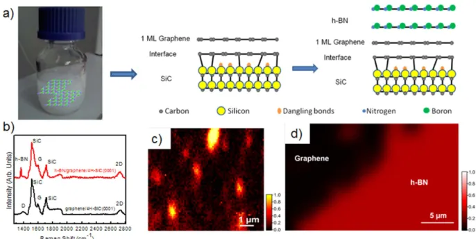
Thermal decomposition of undoped 4H-SiC(0001) can be used to produce large graphene films with a long-range order and high electron mobility14. Monolayer, bilayer, and few-layer graphene on SiC can be obtained by tuning the different experimental parameters (temperature, annealing times, and thickness of SiC substrate)15. The graphene used in this study was obtained by annealing 4H-SiC at 1550 °C in 800 mbar argon for 10 min [see Methods]. The h-BN layers were synthesized using the Polymer Derived Ceramics method by adding lithium nitride (Li3N) micropowders to liquid-state polyborazylene (PBN)13. Incorporating Li3N as a crystallization promoter allows h-BN to crystallise at a lower temperature (1200°C) than under classical conditions (1800 °C)16. The synthesized h-BN layers were then dispersed in ethanol with a low concentration in order to avoid a huge agglomeration of flakes and to control their dispersal over epitaxial graphene. Figure 1(a) presents a schematic illustration of the steps required for the fabrication of the h-BN/graphene structure. After the growth step, the graphene sample was cooled down to room temperature and transfered ex situ from the growth chamber. After ultrasonication of the h-BN suspension, a few drops of solution were deposited on the epitaxial graphene. Raman spec-troscopy was carried out to characterize the morphology of h-BN on graphene. Figure 1(b) compares the micro-Raman spectra of pristine graphene (black line) and the h-BN/graphene heterostructure (red line) in the wavenumber range of 1300–2800 cm−1. Several intense peaks are visible in this range; these correspond to second-order Raman bands originating in the SiC substrate17. In the pristine sample, the graphene contributions are also observed and identified by three main structures: i) the D band at 1370 cm−1, ii) the G band at 1595 cm−1 and iii) the 2D band at 2720 cm−1; the small D peak indicates the high quality of the sample. In the case of h-BN/graphene, we note a new peak at ∼ 1367 cm−1 originating from the E2g mode of h- BN vibration18–20. In Fig. 1(c,d), we observe the integrated intensity Raman map of the h-BN E2g vibration mode for two representative areas of the h-BN/graphene heterostructure. As it is shown by the different colour scale in Fig. 1(c), this area presents small h-BN flakes with a different width (~1–2 μ m). On the other hand, we can also observe the coalescence of various flakes into uniform layers and an abrupt interface between h-BN and the graphene substrate (Fig. 1(d)). As the Raman analysis shows, with the use of the drop-casting method it was not possible to control the thickness of the h-BN flakes and their organization on the epitaxial graphene substrate. However, without the need of a particular treatment, where the h-BN/graphene heterostrucutre was formed, the interface was really abrupt without any interdiffusion. In order to investigate in more detail this interface between the h-BN and epitaxial graphene, STEM/HRTEM experiments were performed. A cross-sectional view was chosen along the (11–20) SiC zone axis. STEM images revealed the thickness of the graphene layers and the detailed crystalline structure of both the h-BN and the graphene (Fig. 2(a), Bright-field STEM and (b) High angle annular dark field (HAADF) STEM). As observed from representative STEM images of our heterostructure, the graphene grown on SiC, produced here, was predominantly composed of few layers. The graphitic layers were atomically flat and showed a continuous film at the step edges. It is obvious from Fig. 2(a), that multilayer stacking of h-BN occurred on the few layer graphene. The measured interlayer distance of about 0.344 ± 0.002 nm, was characteristic of interplanar spacing in h-BN (002) planes21,22. As can be seen in HRTEM of Fig. 2(c), h-BN multilayers were not perfectly flat on the graphene substrate
www.nature.com/scientificreports/
Figure 1. h-BN flakes on graphene/SiC(0001) substrates. (a) Schematic illustration of our method for
growing h-BN/graphene/SiC. After ultrasonication of the h-BN suspension a few drops of the solution were deposited on epitaxial graphene. (b) Comparison of micro-Raman spectra taken on the pristine graphene (black line) and h-BN/graphene (red line) layers. Integrated intensity Raman map of the h-BN E2g vibration
mode for two representative areas of the h-BN/graphene heterostructure (c) area with small h-BN flakes, (d) uniform layers and an abrupt interface between h-BN and the graphene substrate.
Figure 2. (a) Bright-field Scanning Transmission Electron Microscopy (STEM) image and (b) corresponding
High Angle Annular Dark Field (HAADF) STEM image of h-BN on graphene/4H-SiC heterostructure, (c) High-Resolution Transmission Electron Microscopy (HRTEM) image of h-BN on the step edges of graphene on SiC, (d–f) EDX elemental maps showing, respectively, the spatial distribution of C, Si and N in the selected area of the h-BN on graphene/4H-SiC heterostructure. The overlay of the three maps is given in (g).
all over the sample. In different areas, we found that the h-BN layers lay predominately with a misori-entation angle following the (11–20) nanofacets of the SiC substrate. Using Energy-Dispersive X-ray spectroscopy (EDX) we mapped the elemental distribution of C, Si and N in a selected area of the h-BN on graphene/4H-SiC heterostructure (Fig. 2(d–f)). Indeed, a sharp vertical interface between the h-BN Figure 3. (a) XPS overview spectra at hν = 825 eV of the pristine graphene (black line) and the h-BN/
graphene heterostrucuture (blue line). High resolution XPS spectra of h-BN/graphene for (b) C 1s core level, (c) Si-2p core level (d,e) B 1s and N 1s core levels at hν = 825 eV (bulk sensitive, top panel) and hν = 510 eV (surface sensitive, bottom panel).
www.nature.com/scientificreports/
and graphene layers was visible. The intensity of the nitrogen maps across the interface also showed that the sharpness of the graphene/h-BN interface was within 1 nm, corresponding to the spatial resolution of the EDX elemental mapping (due to the thickness sample and the convergence of the electron probe) (Fig. 2(g)). Moreover, from the EDX signal coming from specific spots on the sample we also obtained a quantitative analysis (using the SiC substrate as reference). The average N/B ratio for the whole h-BN region was estimated to be 1.1 ± 0.1, confirming the stoichiometry of the h-BN layer.
To investigate the atomic composition, as well as the chemical bonding environment of our samples, XPS measurements were carried out for the pristine graphene and the h-BN/graphene heterostructure, as shown in Fig. 3. The XPS measurements performed over a wide energy range (hν = 825 eV) showed that the C 1s, Si 2s, and Si 2p peak intensities were not notably affected by the h-BN deposition (Fig. 3(a)), whose presence was confirmed by the B 1s and N 1s core level peaks observed on the h-BN/graphene spectrum. The different contributions to the spectra were extracted by a curve fitting procedure (see Methods). The depth position of the corresponding species across the h-BN/graphene interface was identified by varying the incident photon energy (hv = 510 and 825 eV) and thus changing the surface and bulk sensitivity. The experimental data points are displayed as dots. The solid line is the envelope of the fitted components. The C 1s and Si 2p spectra of the h-BN graphene heterostructure are shown in Fig. 3(b,c), respectively. The C1s spectra show the conventional deconvolution expected for epitaxial graphene on SiC(0001)23–25, characterized by three contributions attributed to the substrate (SiC) at BE = 283.8 eV, the graphene layer (G) at BE = 284.6 eV and the interface layer at 285.3 eV. No evidence of C-B bond at 283. 2 eV26,27 or C-N and C-O bonds expected at higher BE, 286.5 eV28 and 286.2 eV29, respectively, were present in the spectra. These observations confirm that there were no covalent bonds formed between graphene and h-BN, nor graphene contamination. The Si 2p doublet was reconstituted with a 2p1/2:2p3/2 ratio of 0.5 and a spin-orbit splitting of 0.6 eV30. Both spectra consisted of a main Si 2p peak at 101.5 eV. The small shoulder at 102.1 eV was attributed to an interface layer area of the SiC(0001) substrate, while the component at 100.9 eV was attributed to the presence of Si clusters formed when Si-C bonds were broken during graphitization31,32. No additional components related to Si-O bonds29 or Si-N-C (101.9 eV28) were present confirming the formation of a perfect heterostructure between graphene and h-BN, with no evidence of interdiffusion or contamination. XPS spectra of B 1s and N 1s are shown in Fig. 3(c,d), respectively, for two different photon energies (hν = 825 eV and hν = 510 eV). The B1s and N1s spectra exhibited three peaks fitted with Gaussian components (full width at half-maximum,
fwhm ~ 1.4 eV). The main peak at binding energy BE ~ 191 eV for the B 1s and BE ~ 398.6 eV for the N 1s
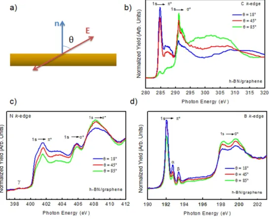
were attributed to B-N bonding, matching those reported for bulk h-BN33–36. The boundaries between h-BN flakes could present a higher density of defects, which could also provide a preferential site for adsorbates (e.g. oxygen). As expected from the first-principle calculations of Orellana et al.37, the most stable defects in h-BN are the self-interstitial Ni and the nitrogen vacancy. Interstitial nitrogen binds strongly with a N atom of the lattice forming a N-N pair37 and the substitution of a nitrogen atom with oxygen is preferred to the substitution of a boron atom because of the closer electronegativity between oxygen and nitrogen atoms. According to the core-level shift model proposed by Caretti et al.38, suggest-ing a core level shift per O substituent N of ~0.8 eV (toward the higher BE) we could attribute the peaks at BE ~ 191.8 eV and 192.6 eV in the B 1s spectra to B-N2O and B-NO2, respectively, (one and two N vacancies are replaced by one and two oxygen). In the case of N 1s, the components at higher BE ~ 399.8 eV and ~401.2 were attributed to O-B-N39 or N-N40 and N-O40,41, respectively. Unoccupied electronic states of the h-BN/graphene heterostructure were also probed by NEXAFS spectroscopy. The C 1s, B 1s and N 1s NEXAFS spectra were measured for different incidence angles of the linear polarized synchrotron light. As shown in Fig. 4(a), we indicate with θ the angle between the polarization vector E and the
surface normal n (θ = 18°, 45° and 85°). Figure 4(b) shows the C 1s NEXAFS spectra. These spectra were
characterized by two sharp resonances at 285.3 eV and 291.7 eV and a broad structure at 292.7 eV. These features were characteristic of pristine graphene on SiC24,42, and were assigned to π *, σ⁎
1 and σ2⁎ reso-nance, respectively. For the grazing incidence of light, when the direction of polarization vector E was
close to the surface normal (θ = 18°), the π* resonance intensity was strongly enhanced. This feature decreased with an increased incident angle and was almost suppressed for normal incidence (θ = 85°). As expected for a planar π conjugated system such as graphene, the σ* resonances revealed the opposite angular dependence behaviour. The sharpness of the NEXAFS features indicated a well-defined bonding environment and a long-range periodic order in the electronic structure. Thus, the NEXAFS spectra unequivocally proved the conservation of sp2 bonds between carbon atoms in the h-BN/graphene het-erostructure. The fact that no modifications were induced on the C 1s NEXAFS spectra with respect to pristine graphene, confirmed the dominant role of van der Waals interactions between graphene and h-BN layers. Figure 4(c,d) show the B 1s and N 1s NEXAFS spectra. In addition to the characteristic B(1s → π *) excitonic transition of h-BN at ~192.0 eV (which is a specific fingerprint of sp2- hybridized B atoms in the hexagonal h-BN network, i.e., a trigonal B-N3 bonding environment) and two σ * peaks at ~198.2 eV and ~199.5 eV, two other excitonic π * peaks were observed in the B 1s x-ray absorption edge at ~192.7 eV and ~193.3 eV38. These peaks, labelled in this study α and β , were assigned to B surrounded by 1 and 2 N-void defects, respectively. Peaks α and β were due to an intermediate situation between B-N3 and B-O3 environments, i.e., B-N2-O and B-NO2, respectively38, confirming the photoemission results. The N 1s NEXAFS spectra displayed an excitonic peak with a maximum centred at ~401.5 eV
Figure 4. (a) Schematic representation of the NEXAFS geometry: θ represents the angle between the
polarization vector E and the surface normal n. (b) carbon (c) nitrogen and (d) boron K-edge, NEXAFS spectra of h-BN/graphene, measured for different incidence angles of the linear polarized synchrotron light. (θ = 18°, 45° and 85°).
Figure 5. (a,b) ARPES measurements of pristine graphene and h-BN/graphene, measured at hν = 60 eV,
through the K-point, in the Γ K direction; (c) ARPES intensity integrated spectra as a function of the binding energy, extracted from the 2D ARPES map, for the initial pristine graphene (red line) and h- BN/graphene (blue line).
www.nature.com/scientificreports/
and two σ * transitions at ~405.8 eV and ~408.1 eV, as found in the literature for a bulk h-BN43,44. Moreover, theoretical calculations predicted an empty level induced by neutral Ni at around 0.6 eV above the valence band maximum (VBM) of h-BN, i.e. just above 397 eV for the 4 eV energy gap of h-BN37,43. Then the small resonance (γ in Fig. 4(c)) observed at about 398.6 eV can be related to this particular defect45, which was also clearly identified in the N 1s XPS spectra. For the orientation of the h-BN flakes on graphene we clearly saw that the flakes were not all perfectly flat on the graphene substrate, as observed in the HRTEM image. In fact, for normal incidence of light and a polarization vector almost in the plane of the sample (θ = 85°), the π* resonance was still visible, even if attenuated with respect to the grazing incidence (θ = 18°).
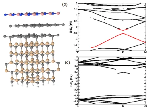
In order to clearly highlight the effect of h-BN on graphene’s electronic structure, ARPES meas-urements were carried out. Figure 5 shows the valence band structure around the K point of the first graphene Brillouin zone, for the pristine graphene layer and the h-BN/graphene heterostructure. On the pristine graphene layer (Fig. 5(a)), the linear dispersion of the π band can be observed. As it has already been observed many times in the case of epitaxial graphene with the Si termination, the π bands formed a cone, for which the π branches crossed at the Dirac point (ED) at − 0.3 eV below the Fermi level (EF). This n-type doping is typical of epitaxial graphene and is due to the charge transfer from the SiC substrate. After h-BN deposition (Fig. 5(b)), these π branches were still clearly defined, proving that the growth of h-BN did not affect the 2D structure of the graphene. The Dirac point was located at − 0.3 eV below the Fermi level, demonstrating the absence of electronic transfer between h-BN and graphene layers, corroborating the absence of an h-BN doped graphene layer. The full width at half maximum (fwhm) of the Dirac cone branches probably increased because of the interaction between the graphene and h-BN layers. It has been proposed that a bandgap would be induced in graphene aligned in a com-mensurate way to a h-BN substrate46. To confirm these features, we performed DFT calculations on the h-BN/graphene van der Waals heterostructure (see Methods). We considered here a commensurate h-BN monolayer on top of a graphene/SiC(0001) substrate (Fig. 6(a)). Structural determinations yielded an h-BN-graphene distance of 3.3 Å with a binding energy of 77 meV/atom, and a graphene-buffer layer of 3 Å, with a binding energy of 166 meV/atom, in agreement with the expected values for such systems. Our DFT calculations confirmed that, in this case, a gap of about ~315 meV is opened at the K point (Fig. 6(b)). This gap opening was due to the electrostatic interaction between the h-BN and the graphene planes, breaking the symmetry of the graphene lattice. Moreover, as shown in (Fig. 6(c)), h-BN main-tained its insulating properties (calculated band gap of ~5.5 eV). In the present case, as the experimental data showed no gap openings for graphene, this suggested the two following hypotheses: (i) the h-BN monolayer was lying with a rotated structure with respect to the graphene plane, preventing from sym-metry breaking (ii) several layers of h-BN were present on graphene, the interaction between the BN planes reducing the electrostatic interaction between h-BN and graphene, which forbids the gap opening. Figure 6. (a) DFT and vdW optimised geometrical structure of the h-BN/graphene/ZLG/SiC van der Waals
Conclusions
In summary, we are able to synthesize a high-quality multilayer h-BN/graphene heterostructure. The h-BN is synthesized by using the PDCs route, from a liquid-state polyborazylene as polymeric precursor additivated with lithium nitride (Li3N) micropowders in order to obtain highly crystallized material. The epitaxial h-BN/graphene domains were shown by micro- Raman spectroscopy. More importantly, the STEM/HRTEM results showed that the h-BN layers are highly crystalline without any interdiffusion. XPS and ARPES spectroscopy shows a sharp interface between graphene and h-BN layers. This demon-strates that epitaxial graphene may be a suitable template to combine with alternative vdW solids due to its lack of dangling bonds, chemical inertness, and ability to remain intact under high stress. This study demonstrates a simple and efficient route for the controlled fabrication of multilayered graphene/h-BN heterostructures with promising applications in nanoelectronics.
Methods
The h-BN on graphene/4H-SiC(0001) (Si-face, 4° off towards [11–20]) (Si-face) was created in two stages: first few-layer graphene was produced on a 4H-SiC(0001) commercial wafer off-axis. The sample was heated to 1100 °C in a UHV (10−5 mbar) and then further heated to 1550 °C in an Ar atmosphere for 10 mn. It was then cooled down to room temperature and transferred ex-situ from the growth cham-ber to the analysis chamcham-ber. The h-BN layers were synthesized using the Polymer Derived Ceramics route by adding lithium nitride (Li3N) micropowders to liquid-state polyborazylene (PBN), as recently described13. The synthesized h-BN layers were then dispersed in ethanol and a few drops of the latter solution were deposited on the epitaxial graphene. Cross-sectional TEM samples were prepared using a focused ion beam (FIB). Protective layers of amorphous carbon were deposited on the sample, initially with the electron beam to avoid surface damage. The HRTEM/STEM studies were done on a Jeol 2200FS microscope working at 200 kV and equipped with an aberration corrector for the probe (STEM mode) and an Ultra-High Resolution (UHR) pole piece.
XPS/ARPES experiments were carried out on the TEMPO beamline47 (SOLEIL French synchrotron facility) at low temperature (~120 K). The HU80 Apple II undulator was set to deliver linearly polarized light. The photon energy wes selected using a high-resolution plane grating monochromator, with a resolving power E/Δ E that can reach 15000 over the whole energy range (45–1500 eV). During the XPS measurements, the photoelectrons were detected at 0° from the sample surface normal n and at 46° from the polarization vector E. A Shirley background was subtracted in all core level spectra. The C 1s spectra were fitted by a sum of a Gaussian function convoluted with a Doniach-Sunjic lineshape. An asymmetry factor α was used, where α = 0.1 eV (peak G) and α = 0 eV (SiC an IL). The graphene thickness was calculated from the ratio between the intensity of the G and SiC components48,49 extracted from XPS data using the following equation: d( ) =Å λ⋅ cos θ⋅ ln 1
(
+ IIG ⋅ NN)
SiC SiC
G . For a photon energy of 510 eV
we had an escape depth λ of 7.2 Å. In the geometry of our XPS experiment the take-off angle θ was 0° and IG and ISiC represented the area of the G and SiC components of the C 1s peak extracted from the
deconvolution. For epitaxial graphene on SiC, the areal density of the C atom in graphene NG was about
three times that of C atoms in SiC49. We obtained a thickness d = 14.9 Å corresponding to about 6 ML of graphene. The Si 2p spectra were fitted by sums of Voigt curves, that is, the convolution of a Gaussian (of full-width at half-maximum GW) by a Lorentzian (of full-width at half-maximum LW). Where the LW are fixed at 45 meV50. In the case of B 1s and N 1s, the peaks were fitted by the sum of Gaussian functions (full width at half-maximum, fwhm ~ 1.4 eV). For ARPES measurements, the photon energy (hν = 60 eV) and sample orientation were set in order to explore the k-space region around the K point in the Γ K direction of the Brillouin zone. The spot size was 100 × 40 (H × V) μ m.
Ab initio calculations to describe the electronic structure of the h-BN/graphene van der Waals
het-erostructure were performed using a very efficient DFT localized orbital molecular dynamic technique (FIREBALL)51. Basis sets of sp3d5 for B, sp3 for C, N and Si, and s for H were used with cutoff radii (in atomic units) s = 4.5, p = 4.9, d = 5.2 (B), s = 4.5, p = 4.5 (C), s = 4.2, p = 4.2 (N), s = 4.8, p = 5.4 (Si) and s = 4.1 (H)52. In this study we considered a supercell of 5 ML SiC(0001), with a zero-layer graphene and an AB stacked graphene plane on top. The lateral size roughly corresponded to a 4× 4 unit cell of graphene. The bottom layer was saturated with hydrogen atoms. On top of the supercell, we set an h-BN monolayer. The geometry of the system was then relaxed at 0 K, using a sample of 32 k-points in the Brillouin zone, maintaining the last three bottom layers in bulk positions53. The final distance between the 2D material planes was determined using the well-known LCAO-S + vdW formalism54, which spe-cifically takes into account van der Waals interaction in the frame of DFT. A set of 300 special k points along the Γ –K-M path was used for the band structure calculations on the optimized geometry. Finally, a gap correction of 1.18 was applied, in order to correct the well-known DFT deficiency and to get a better agreement with the experiments, following the method proposed by Park et al.55.
References
1. Geim, A. K. & Grigorieva, I. V. Van der Waals heterostructures. Nature 499, 419–425 (2013).
2. Dean, C. R. et al. Boron nitride substrates for high-quality graphene electronics. Nat. Nanotechnol. 5, 722–726 (2010). 3. Lee, G.-H. et al. Electron tunneling through atomically flat and ultrathin hexagonal boron nitride. Appl. Phys. Lett. 99, 243114
www.nature.com/scientificreports/
4. Watanabe, K., Taniguchi, T. & Kanda, H. Direct-bandgap properties and evidence for ultraviolet lasing of hexagonal boron nitride single crystal. Nat. Mater. 3, 404–409 (2004).
5. Ju, L. et al. Photoinduced doping in heterostructures of graphene and boron nitride. Nat. Nanotechnol. 9, 348–52 (2014). 6. Sutter, P., Cortes, R., Lahiri, J. & Sutter, E. Interface Formation in Monolayer Graphene-Boron Nitride Heterostructures. Nano
Lett. 12, 4869–4874 (2012).
7. Kim, S. M. et al. Synthesis of Patched or Stacked Graphene and hBN Flakes: A Route to Hybrid Structure Discovery. Nano Lett. 13, 933–941 (2013).
8. Liu, Z. et al. Direct Growth of Graphene/Hexagonal Boron Nitride Stacked Layers. Nano Lett. 11, 2032–2037 (2011).
9. Liu, Z. et al. In-plane heterostructures of graphene and hexagonal boron nitride with controlled domain sizes. Nat. Nanotechnol. 8, 119–124 (2013).
10. Lalmi, B. et al. Flower-shaped domains and wrinkles in trilayer epitaxial graphene on silicon carbide. Sci. Rep. 4, 4066 (2014). 11. Lin, Y.-C. et al. Direct synthesis of van der Waals solids. ACS Nano 8, 3715–23 (2014).
12. Lin, Y. et al. Atomically Thin Heterostructures Based on Single-Layer Tungsten Diselenide and Graphene. Nano Lett. 14, 6936–6941 (2014).
13. Yuan, S., Toury, B. & Journet, C. & Brioude, A. Synthesis of hexagonal boron nitride graphene-like few layers. Nanoscale 6, 7838–41 (2014).
14. Pallecchi, E. et al. High Electron Mobility in Epitaxial Graphene on 4H-SiC(0001) via post-growth annealing under hydrogen.
Sci. Rep. 4, 4558 (2014).
15. Boutchich, M. et al. Atmospheric pressure route to epitaxial nitrogen-doped trilayer graphene on 4H-SiC (0001) substrate. Appl.
Phys. Lett. 105, 233111 (2014).
16. Yuan, S. et al. Low-Temperature Synthesis of Highly Crystallized Hexagonal Boron Nitride Sheets with Li 3 N as Additive Agent.
Eur. J. Inorg. Chem. 2014, 5507–5513 (2014).
17. Ni, Z. et al. Raman spectroscopy of epitaxial graphene on a SiC substrate. Phys. Rev. B 77, 115416 (2008). 18. Geick, R., Perry, H. & Rupprecht, G. Normal Modes in Hexagonal Boron Nitride. Phys. Rev. 146, 543–546 (1966).
19. Song, L. et al. Large Scale Growth and Characterization of Atomic Hexagonal Boron Nitride Layers. Nano Lett. 10, 3209–3215 (2010).
20. Shi, Y. et al. Synthesis of Few-Layer Hexagonal Boron Nitride Thin Film by Chemical Vapor Deposition. Nano Lett. 10, 4134–4139 (2010).
21. Pakdel, A., Bando, Y. & Golberg, D. Nano boron nitride flatland. Chem. Soc. Rev. 43, 934–59 (2014).
22. Pauling, L. The Structure and Prperties of Graphite and Boron Nitride. Proc. Natl. Acad. Sci. USA 56, 1646–1652 (1966). 23. Coletti, C. et al. Large area quasi-free standing monolayer graphene on 3C-SiC(111). Appl. Phys. Lett. 99, 081904 (2011). 24. Ouerghi, A. et al. Large-area and high-quality epitaxial graphene on off-axis SiC wafers. ACS Nano 6, 6075–6082 (2012). 25. Emtsev, K. V., Speck, F., Seyller, T., Ley, L. & J. D., R. Interaction, growth, and ordering of epitaxial graphene on SiC{0001}
surfaces: A comparative photoelectron spectroscopy study. Phys. Rev. B 77, 155303 (2008).
26. Mannan, M. A. et al. Hexagonal Nano-Crystalline BCN Films Grown on Si (100) Substrate Studied by X-Ray Absorption Spectroscopy. Mater. Sci. Appl. 04, 11–19 (2013).
27. Komatsu, T. Bulk synthesis and characterization of graphite-like B-C-N and B-C-N heterodiamond compounds. J. Mater. Chem. 14, 221 (2004).
28. Velez-Fort, E. et al. Epitaxial Graphene on 4H-SiC ( 0001 ) Grown under Nitrogen Flux : Evidence of Low Nitrogen Doping and High Charge Transfer. ACS Nano 6, 10893–10900 (2012).
29. Velez-Fort, E. et al. Atomic oxidation of large area epitaxial graphene on 4H-SiC(0001). Appl. Phys. Lett. 104, 093109 (2014). 30. Landemark, E., Karlsson, C. J., Chao, Y.-C. & Uhrberg, R. I. G. Core-Level Spectroscopy of the Clean Si(001) Surface: Charge
Transfer within Asymmetric Dimers of the 2 × 1 and c(4 × 2) Reconstructions. Phys. Rev. Lett. 69, 1588–1591 (1992).
31. Riedl, C., Coletti, C. & Starke, U. Structural and electronic properties of epitaxial graphene on SiC(0 0 0 1): a review of growth, characterization, transfer doping and hydrogen intercalation. J. Phys. D. Appl. Phys. 43, 374009 (2010).
32. Silly, M. G. et al. Electronic and structural properties of graphene-based metal-semiconducting heterostructures engineered by silicon intercalation. Carbon N. Y. 76, 27–39 (2014).
33. Shimoyama, I., Baba, Y., Sekiguchi, T. & Nath, K. NEXAFS spectra of an epitaxial boron nitride film on Ni(1 1 1). J. Electron
Spectros. Relat. Phenomena 137–140, 573–578 (2004).
34. Lei, W., Portehault, D., Dimova, R. & Antonietti, M. Boron carbon nitride nanostructures from salt melts: tunable water-soluble phosphors. J. Am. Chem. Soc. 133, 7121–7 (2011).
35. Ci, L. et al. Atomic layers of hybridized boron nitride and graphene domains. Nat. Mater. 9, 430–435 (2010).
36. Gwangwoo, K. et al. Growth of High-Crystalline, Single-Layer Hexagonal Boron Nitride on Recyclable Platinum Foil. Nano Lett. 13, 1834–1839 (2013).
37. Orellana, W. & Chacham, H. Stability of native defects in hexagonal and cubic boron nitride. Phys. Rev. B 63, 125205 (2001). 38. Caretti, I. & Jimé nez, I. Point defects in hexagonal BN, BC3 and BCxN compounds studied by x-ray absorption near-edge
structure. J. Appl. Phys. 110, 023511 (2011).
39. Li, J., Li, J., Yin, Y., Chen, Y. & Bi, X. Water-assisted chemical vapor deposition synthesis of boron nitride nanotubes and their photoluminescence property. Nanotechnology 24, 365605 (2013).
40. Sugino, T., Tai, T. & Etou, Y. Synthesis of boron nitride film with low dielectric constant for its application to silicon ultralarge scale integrated semiconductors. Diam. Relat. Mater. 10, 1375–1379 (2001).
41. Pan, W. J. et al. Preparation of thin films of carbon-based compounds. Appl. Surf. Sci. 218, 298–305 (2003).
42. Aristov, V. Y. et al. Graphene synthesis on cubic SiC/Si wafers. perspectives for mass production of graphene-based electronic devices. Nano Lett. 10, 992–5 (2010).
43. Petravic, M., Peter, R., Fan, L.-J., Yang, Y.-W. & Chen, Y. Direct observation of defects in hexagonal boron nitride by near-edge X-ray absorption fine structure and X-ray photoemission spectroscopy. Nucl. Instruments Methods Phys. Res. Sect. A Accel.
Spectrometers, Detect. Assoc. Equip. 619, 94–97 (2010).
44. Caretti, I. & Jiménez, I. Composition and bonding structure of boron nitride B1− xNx thin films grown by ion-beam assisted evaporation. Chem. Phys. Lett. 511, 235–240 (2011).
45. Peter, R. et al. Formation of defects in boron nitride by low energy ion bombardment. J. Appl. Phys. 106, 083523 (2009). 46. Woods, C. R. et al. Commensurate–incommensurate transition in graphene on hexagonal boron nitride. Nat. Phys. 10, 451–456
(2014).
47. Polack, F. et al. TEMPO: a New Insertion Device Beamline at SOLEIL for Time Resolved Photoelectron Spectroscopy Experiments on Solids and Interfaces. AIP Conf. Proc 1234, 185–188 (2010).
48. Penuelas, J., Ouerghi, A., Lucot, D., David, C. & Gierak, J. Surface morphology and characterization of thin graphene films on SiC vicinal substrate. Phys. Rev. B 79, 033408 (2009).
49. Seyller, T. et al. Structural and electronic properties of graphite layers grown on SiC(0001). Surf. Sci. 600, 3906–3911 (2006). 50. Bozek, G. M. Bancroft, J. D., Cutler, J. N. & Vibrationally, K. H. T. Resolved Core-Level Photoelectron Spectroscopy: Si 2p
51. Lewis, J. P. et al. Advances and applications in the FIREBALLab initio tight-binding molecular-dynamics formalism. Phys. Status
Solidi 1989–2007 (2011), doi: 10.1002/pssb.201147259.
52. Basanta, M. A., Dappe, Y. J., Jelínek, P. & Ortega, J. Optimized atomic-like orbitals for first-principles tight-binding molecular dynamics. Comput. Mater. Sci. 39, 759–766 (2007).
53. Pierucci, D. et al. Self-organized metal-semiconductor epitaxial graphene layer on off-axis 4H-SiC(0001). Nano Res. 8, 1026–1037 (2015).
54. Dappe, Y., Ortega, J. & Flores, F. Intermolecular interaction in density functional theory: Application to carbon nanotubes and fullerenes. Phys. Rev. B 79, 165409 (2009).
55. Park, C.-H., Giustino, F., Cohen, M. & Louie, S. Velocity Renormalization and Carrier Lifetime in Graphene from the Electron-Phonon Interaction. Phys. Rev. Lett. 99, 086804 (2007).
Acknowledgements
This work was supported by ANR SUPERTRAMP grants. We acknowledge support from GANEX (Grant No. ANR-11-LABX-0014) and Labex “Nanosaclay (Grant No. ANR-10-LABX-0035)”. GANEX belongs to the public funded “Investissements d’Avenir” programme managed by the French National Research Agency.
Author Contributions
H.S., D.P. and M.H., grew the graphene sample and conducted the measurements by XPS/ARPES and NEXAFS, H.S., M.H. and H.H. characterised it by Raman spectroscopy. B.T. and S.Y. synthesised the h-BN flakes. D.P., M.S., H.S., M.H., F.S., M.B. and A.O. analysed the data. G.P. carried out the STEM/ HRTEM experiment. Y.J.D. carried out the DFT band structure. B.M. carried out supplementary Raman spectroscopy and R.B. supported the experiment. A.O., M.B., Y.J.D. and D.P. wrote the paper with all authors contributing to the final version. A.O. planned the experiments and supervised the project.
Additional Information
Competing financial interests: The authors declare no competing financial interests.
How to cite this article: Sediri, H. et al. Atomically Sharp Interface in an h-BN-epitaxial graphene van
der Waals Heterostructure. Sci. Rep. 5, 16465; doi: 10.1038/srep16465 (2015).
This work is licensed under a Creative Commons Attribution 4.0 International License. The images or other third party material in this article are included in the article’s Creative Com-mons license, unless indicated otherwise in the credit line; if the material is not included under the Creative Commons license, users will need to obtain permission from the license holder to reproduce the material. To view a copy of this license, visit http://creativecommons.org/licenses/by/4.0/