HAL Id: hal-02565595
https://hal.archives-ouvertes.fr/hal-02565595
Submitted on 6 May 2020
HAL is a multi-disciplinary open access
archive for the deposit and dissemination of sci-entific research documents, whether they are pub-lished or not. The documents may come from teaching and research institutions in France or abroad, or from public or private research centers.
L’archive ouverte pluridisciplinaire HAL, est destinée au dépôt et à la diffusion de documents scientifiques de niveau recherche, publiés ou non, émanant des établissements d’enseignement et de recherche français ou étrangers, des laboratoires publics ou privés.
A highly sensitive microsystem based on
nanomechanical biosensors for genomics applications
L.M. Lechuga, J. Tamayo, M. Alvarez, L.G. Carrascosa, A. Yufera, R. Doldan,
E. Peralias, A. Rueda, J.A. Plaza, K. Zinoviev, et al.
To cite this version:
L.M. Lechuga, J. Tamayo, M. Alvarez, L.G. Carrascosa, A. Yufera, et al.. A highly sensitive mi-crosystem based on nanomechanical biosensors for genomics applications. Sensors and Actuators B: Chemical, Elsevier, 2006, 118 (1-2), pp.2-10. �10.1016/j.snb.2006.04.017�. �hal-02565595�
A HIGHLY SENSITIVE MICROSYSTEM BASED ON
NANOMECHANICAL BIOSENSORS FOR GENOMICS
APPLICATIONS
L.M. Lechuga1*, J.Tamayo1, M. Álvarez1, L.G. Carrascosa1, A. Yufera1, R. Doldán1, E. Peralías, A. Rueda1, J.A. Plaza1, K. Zinoviev1 and C Domínguez1, A. Zaballos2, M.
Moreno2 and C. Martínez-A2, D. Wenn 3, N. Harris3, C. Bringer4,V. Bardinal4, T. Camps, C. Vergnenègre4 and C. Fontaine4 ,V. Díaz5 and A. Bernad.5
1Microelectronics National Center. CSIC. Spain 2Biotechnology National Center (CNB). CSIC. Spain.
3 ECS, University of Southampton, UK 4LAAS-CNRS, France
5 GENETRIX, S.L, Spain
Abstract
Microcantilever based biosensors are a promising tool to detect biomolecular interactions in a direct way with high accuracy. We show the development of a portable biosensor microsystem able to detect nucleic acid hybridization with high sensitivity. The microsystem comprises an array of 20 micromechanical cantilevers produced in silicon technology, a polymer microfluidic system for delivery of the samples, an array of 20 vertical cavity surface emitting lasers (VCSELs) with collimated beams thanks to an integrated microlens array, an optical coupling element to provide the optical path required, and chips with the photodetectors and the CMOS circuitry for signal acquisition and conditioning, capable of measuring the cantilever deflection with sub-nanometer resolution. Robust immobilization and regeneration procedures have been implemented for the oligonucleotide receptor sequences. In a further innovation, an optical waveguide cantilever transducer has been also developed in order to improve the final performance of the device. This has a number of advantages in terms of a simple optical geometry and improved sensitivity.
Keywords: biosensor, microsystem, Si technology, microcantilevers, DNA biochip.
*corresponding author:
Tel: +34 918060700, Fax: +34 918060701
Introduction
There is an increasing interest in systems based on micro/nanotechnologies for ultrasensitive and miniaturised biosensors and biochips. The application of this new micro- and nanotechnology techniques to microarray production will result in both miniaturization of biochip and an increase in sensitivity of the assays. One of the most promising approaches in micro/nanobiosensors is in the area of cantilever based sensors, which are a new class of highly sensitivity devices able of performing local, high resolution and label-free molecular recognition measurements [1, 2]. These sensors derive from the microfabricated cantilevers used in atomic force microscopy [3] and are based on the bending induced in the cantilever when, for example, a biomolecular interaction takes place on one of its surfaces. The microcantilevers translate the molecular recognition of biomolecules into a nanomechanical motion [4] (from a few to hundreds of nanometres), that is commonly coupled to an optical or piezoresistive read-out system[5-7] (see Fig. 1 for details). These devices can specifically detect single-base mismatches in oligonucleotide hybridisation [4] among other interesting applications. In these assays [5], nucleic acids are immobilized only on one side of a micromachined cantilever [8]. Exposure of the cantilever to a sample containing complementary nucleic acid gives rise to a cantilever bending [9] of a few nanometers. The nanomechanical response is due to the surface stress change of the active side with respect to the other side, in which DNA is not immobilized [10]. Surface stress arises from the electrostatic, van der Waals and steric intermolecular interactions on the surface [11]. The deflection is measured with sub-nanometer resolution by an optical system in which a laser beam reflects off the surface of the cantilever and is detected by a custom position sensitive photodetector.
In this paper we show the development of a portable multibiosensor microsystem based on microcantilever sensors able to detect hybridization of nucleic acids partly complementary to human genes with high sensitivity. The biosensor microsystem consists of: i) an array of twenty microcantilevers as biosensing tranducers, ii) an optical detection system (lasers and photodetectors) capable of measuring the cantilever movement with sub-nanometer resolution and iii) a polymer microfluidic system for reagents delivery to the sensor surface [12].
In order to obtain the biosensor microsystem the main steps to be accomplished are: the fabrication of arrays of 20 microcantilevers, the development of a self-assembly chemistry for the DNA probe immobilization, the fabrication of a polymer microfluidic header
integrated with the cantilever array, the development of an optical detection subsystem with a monolithic array of 20 single mode oxide-confined VCSELs and a coupling element, the integration of an array of 20 segmented photodetectors and CMOS circuits for the detection and processing of the laser beam displacement, and finally, the assembly of the different components with an accurate alignment. To our knowledge, this device will be the first biosensor microsystem based on nanomechanics, in which sensors, optical detection system and microfluidics will be integrated making available this device for clinical testing. The microsystem is intended to be used initially for the detection of mutations and polymorphisms of the BRCA1 human gene involved in the development of breast cancer, but has many other applications in the biodiagnostic and environmental areas.
1. Fabrication of the microcantilever array transducer
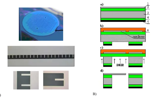
Silicon, silicon nitride and silicon oxide cantilevers are available commercially with different shapes and sizes in analogy to AFM cantilevers. The reported technologies allow the fabrication of ultra thin cantilevers of up to 12 nm thick [13] and millions of them on one wafer [14] with typical lengths between 10 and 500 µm. However, for a specific biosensor application the cantilever geometry, dimensions and materials have been modelled in order to obtain a highly sensitive nanomechanical response with a small sensor area. The thickness, length, and width of the cantilever to be fabricated are derived from the modeling using Finite element simulations (ANSYS). Reducing the thickness and increasing the length results in increment of sensitivity of the device but also leads to complexity in fabrication technology. A fabrication technology of single-crystalline-silicon thin cantilevers using commercially available Silicon-On-Insulator (SOI) wafers has been developed and optimized with the objective to achieve 100% yield of cantilevers per wafer. It has been possible to fabricate arrays of thousands of identical cantilevers on one wafer. The technology allows to fabricate arrays of 20 cantilevers with discrete and common windows, each being 200 or 100 μm long, 40 μm wide, and 340 nm thick (see Figure 2a).
The sequence of the fabrication technological steps is shown in Fig.2B. The front side contained a structural silicon layer (1) and a sacrificial silicon oxide layer (2). The back side of the silicon substrate (3) has a silicon oxide layer (4). As a first step, the back side was covered with an aluminium layer (5) as a mask material for DRIE. The initial multi-layer structure used for the fabrication of cantilevers is presented in Fig. 2a. Afterwards, cantilevers on the front side were formed by dry etching of silicon layer through the pattern obtained by photolithography. Finally, the silicon oxide was removed from the areas where the silicon
substrate must be etched. Before the next step the components side was covered with a photoresist layer (6). Etching the holes in 450 µm thick silicon substrate with DRIE takes about one hour. The etching gives almost vertical walls in the cavities with small, about 20 µm, lateral undercut at the top. At this stage, clean silicon oxide membranes with cantilevers and photoresist layer on top were obtained (see Fig. 2B). The photoresist layer 6 prevented the membranes of cracking and allows to obtain 100 % yield of the production (among 2500 cantilevers per wafer). The membranes were etched in vapours of HF (49%) to release the cantilevers. Afterwards wafers were shortly rinsed with DI water. Finally, the photoresist film was removed by oxygen plasma etching.
The mechanical properties of the cantilevers have been experimentally determined (see Table 1). The spring constant of cantilevers were evaluated using a calibrated AFM probe. In addition, the harmonic characterisation of the cantilevers was also done. The experimental results match with the simulated ones when the overetching of the cantilevers is considered. The measured resonance frequencies are also in good agreement with the calculated ones. The Q factors are a little smaller than the Q factor of commercial ones, however this is in good agreement with the results obtained in published works for very thin cantilevers.
2. Immobilization and regeneration protocols.
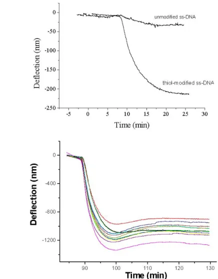
The oligonucleotides receptors must be bound to the cantilever surface by an extremity and separated from the surface to facilitate the duplex formation of the nucleotides closer to the surface. This has been achieved through the development of a self-assembly chemistry which allows the addressing of DNA immobilization at the nanometer-scale level only on one side of the cantilever array. The density will be tuned by using spacer molecules with a terminal group that inhibits non-specific adsorption. The optimised immobilisation procedure is based on thiolated self-assembled monolayers. Figure 3 shows the bending of the cantilevers observed during the immobilisation of the oligonucleotide receptors. Due to the attractive interaction between the nucleotide chain and the gold, the most favourable structure for adsorbed thiolated DNA monolayer is the DNA strongly anchored at the surface by the thiol linker and with the nucleotide chain in contact with the surface. To enhance the accessibility of the DNA probes to the target and assures that the DNA probes are only attached to the gold surface through the terminal sulphur atom of the thiol linker, the surface was exposed to 6-mercapto-1-hexanol (MCH) after DNA immobilization (see Figure 3). MCH adsorption produces a large compressive surface stress, giving a downwards bending of about 30-35% of the cantilever deflection resulting from the thiolated DNA immobilisation [11].
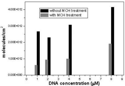
To understand the effects of the MCH treatment, we performed radiolabelling experiments, (see Figure 4) using the thiol modified DNA radioactively labelled. The quantification of the immobilized DNA before and after the MCH treatment was carried out with a scintillation counting. The results indicate that the MCH molecules displace about 60% of the immobilized DNA, suggesting that only 40% of the immobilized chains are covalently attached to the gold surface of the cantilever[11].
3. Microfluidics system.
A polymer microfluidic flow cell has been developed which integrates with the cantilever array. The flow cell incorporates a single flow channel to allow the delivery of reagents to the array of cantilevers, and subsequent removal to waste. The flow cell is required to be a low-cost disposable item. It consists of three acrylic layers and two PDMS gaskets. The acrylic layers are directly machined on a Datron CAT 3D M6 micromill and include recesses for the gaskets and the cantilever chip. In order to produce the PDMS gaskets, a mould tool was machined directly into brass. The PDMS is mixed and then forced into the assembled mould using a syringe. The mould is then placed into an oven at 90°C for one hour to cure the PDMS. The cantilever chip is mounted into a recess in one of the acrylic layers using UV-curing adhesive. After this, the oligonucletide receptors are immobilised on the individual cantilevers using traditional micro-spotting or ink-jet printing techniques.
The assembled flow cell is shown in figure 5. This flow cell plugs onto a non-disposable base unit, which consists of three fluid ports and two metal guide pins, as shown in figure y. One of the fluid ports is the inlet, one is the outlet, and the third acts as a priming port in order to remove any air bubbles from under the cantilever chip. When the flow cell is pressed onto the base unit, the vertical tubes on the base unit that transport the fluids locate into holes in the PDMS gasket and form a seal (Figure 5B). In this way, the flow cell may be removed from the base unit and a new flow cell attached very simply and quickly. The liquid volume in the flow cell is about 25μl.
This flow cell has a single common fluid path that addresses all of the cantilevers in the array. A variant on this flow cell is currently being developed which has a discrete fluid path to each cantilever. This presents a much greater challenge but will allow the immobilisation to be performed on individual cantilevers by flowing solutions through the appropriate channel. The immobilisation process can also potentially be monitored in real-time if the flow cell is connected to the optical system.
discrete fluid channels with 250µm pitch; alignment of the cantilever chip to the fluid channels in an acrylic layer; gluing and sealing of the cantilever chip to the acrylic layer ensuring that there is no leakage path between adjacent cantilevers; making multiple reversible fluid connections to the header in a rapid and reliable way; and finally ensuring a good optical path to and from the cantilever surface.
4. Optical subsystem for excitation.
The development of an optical detection subsystem must integrate all of the required elements with the necessary alignment accuracy of the VCSEL, cantilever and photodetector arrays. The design and fabrication of the optical subsystem takes into account several requirements: size specifications, expected beam deflection on photodetector, efficient light injection and collection, the requirement for a coupling element, as well as the control of the output beam which tends to diverge along propagation. For that reason, an original optical subsystem has been implemented, which enables to target accurately each cantilever following the parallelism of the arrays and the microfluidics, amplifying the cantilever deflection without any resonant measurement.
The optical subsystem consists of a 20 single-mode oxide-confined amplifying VCSEL (Vertical Cavity Surface Emission Lasers) array emitting at 850 nm through a 5.5μm AlOx diameter. The divergence of these mono-mode sources is around 22º FWHM, which means that their divergence has to be decreased in order to enlarge the cross talk free propagation distance that have been fabricated (see Figure 6A). In addition, a microlens array must be used to collimate the optical beams. The best lens design has been calculated to have, for a PMMA lens, a focal length of 257μm F/#: 1.71. The beam divergence after such a customized lens, located 263μm far from the VCSEL source, has been measured to be about 1.5°.
The DNA hybridisation induces a weak surface stress of the cantilever used as a transducer. During the system operation, cantilevers are lighted by the VCSEL laser sources described above. The beam deflection originated from this stress is very small and need to be amplified in order to be detected. The deflection angle of the cantilever is a function of its length: the longer the cantilever is, the bigger the reflection angle. For the minimum level to be detected, the cantilever end moves in the nanometer range, which results in a deflection angle around 0.28 mdeg for a 200μm long cantilever. The simplest way to detect the cantilever movement is to place a photodetector far enough so that the spot displacement on the sensitive surface exceeds the position resolution of the detection device, as routinely used in AFM equipments. However, this solution hinders the miniaturization of the whole biosensor system so in order to ensure the compactness of the whole system, a coupling element has been fabricated, in
which the deflected beam propagates through the air, and whose structure is at the same time the mechanical support frame for the global system. Its consists of two parallel one-side metallized and SiO2 protected silicon wafers separated by air, mounted on a high speed machined metallic support. The minimum propagating beam path should be equal to 10cm to get reach to required sensitivity. For an incident angle of 10° and for a mirror separation of 1cm, such a path is obtained for a coupler length of 2cm. The principle of the coupling element is shown in Figure 6B.
Electro-Optical subsystem for detection and data acquisition.
For the detection of the displacement of the laser beam reflected off the cantilever backside, an array of 20 photodetectors is used. The Position Sensing Detector (PSD) is employed to measure changes on the position of the light spot emitted by a VCSEL cell. The process is illustrated in Fig. 7 where a gaussian distribution of the laser power on the
photodetector array is assumed with an elliptic spot with dimensions Rx =3σx and Ry = 3σy (σx
and σy are the standard deviation of the gaussian). When biomolecular interaction takes place,
the cantilever deflection (d) goes from the initial value (d0) to other (d1), provoking a displacement of the Spot Centre (SC) from its initial location (SC0) to the new one (SC1).
In general, an area image sensor consists of an array of pixels, each containing a photodetector that converts incident light into photocurrent and some of the readout circuits needed to convert the photocurrent into electric charge or voltage and to read it off the array. PSD systems[15][16][17] track spot paths along a photodetection surface. This tracking is characteristic of a sensing process, that in our case it must be in the range from sub-micrometers up to few tens of micrometer. Thus, the photodetectors and the proposed detection algorithm have been designed and optimized to obtain this resolution. Since the form of the spot is assumed invariant the spot centre (SC) is considered as a good candidate to study the spot movement. However, for some standard pixel sizes, the SC could be always inside a pixel and the required resolution in our application is below the pixel size. With this in mind, an algorithm for the PDS is proposed in this paper divided into the two following steps.
• Step1: Final result for step 1 is that a two-dimensional array of voltages (frame) is generated. With this information, the pixel where the spot is will be known, having a resolution of the SC position equal to the pixel size, or equivalently, a pixel resolution system.
• Step2: To increase the accuracy of the measurement, the centroid of the spot is calculated using a subset of the acquired frame according to step 1, which is an
approximation of the SC.
A 128 x 16 pixel array system for PSD was designed. It is implemented in a CMOS
technology and is composed of a pixel array, control digital circuitry, analog processing and output buffers. In CMOS there are several classical structures for optical power to current conversion, based mainly on diodes and bipolar transistors as photodetection devices. A pdiff-nwell photodiode structure is chosen in this case to isolate as much as possible the photocurrent in each pixel. For the signal pixel array, the well known Active Pixel Sensor
(APS) [18] structure, shown in Figure 8A is used. It performs two basic operations: when
transistor Mres is switched on, Vpixel is updated to voltage Vinipix, while for Mres off, the photocurrent is integrated in the parasitic capacitor in node Vpixel (see Figure 8.(b)), which is approximately the photodiode capacitor. Transistor Mseg works as a voltage follower and
Msw is used to connect/disconnect the pixel to the vertical bus (for columns) which connects
all pixels in a column.To correct the influence of the main sources of noise in APS based system, the Correlated Double Sampling (CDS) [19][20] technique is used. It is based on sampling two times the APS output: the first, when Mres is switched off, and the second, at the end of the integration interval. The difference will cancel the noise and also will eliminate the non-zero substrate effect of Mres threshold voltage. The schematic in Figure 8.(c) shows the CDS circuits used. The branch controlled by SHR takes samples of the signals immediately after the reset signal is activated, and the branch controlled by SHS does it at the end of the integration interval. The voltage Voutj = VoutSj - VoutRj is obtained at the CDS output. Since there is a CDS circuit for each column, the outputs are multiplexed to obtain the frames.
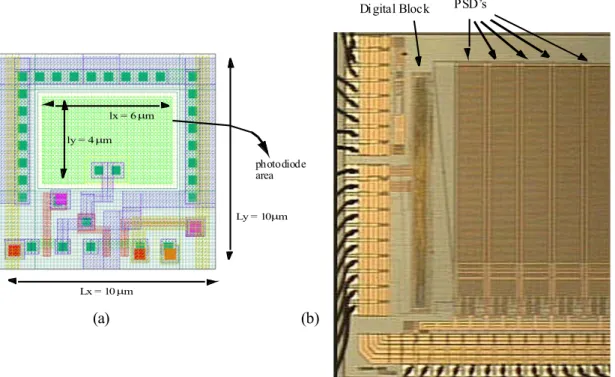
The system has been designed in a 0.35 μm CMOS technology, 2 polys and 4 metals. The layout of the 10 μm x 10 μm pixel is shown in Figure 9.(a), the size of the photodiode is 4 μm x 6 μm, therefore the fill factor is 24 %. A microphotograph of the fabricaded chip is in
Figure 9B, where only 5 of the 20 PSDs are shown. Preliminary experimental results are
shown in Figure 10 giving resolutions under 2 μm, which is agreement with the precission of the used micrometer.
6. Final integration and packaging.The final integration of the whole system is being performed by incorporating the microfluidic header into an optical sub-system which includes the optical sources, coupling element, position sensing photodetectors and mechanical
alignment stages. This sub-assembly, shown in Figure 11, is mounted in an instrument that incorporates fluid components, power supplies, temperature control, data acquisition and CMOS control electronics.
7. Optical Waveguide Cantilevers.
In order to achieve further integration an optical cantilever sensor has been implemented. The detection method is based on monitoring the light exiting the microcantilever. This integrated waveguide cantilever sensor can be fabricated as array of independent waveguide channels designed for monitoring of bio-specific reactions. The sensor can work in static or in dynamic modes, either by monitoring the deflection or by monitoring the changes in the resonance frequency of the cantilever. The advantage of the device is that the transducer is integrated with the receptor on one chip, the complete optical system is in the plane of the cantilever chip, and only a simple external photodetector is required for measuring the optical output power. No preliminary alignment or adjustment is needed, except for light coupling into the chip, which does not affect seriously the performance of the device if the coupler is well designed. The sensitivity of the device is comparable to the one of the AFM principle based instruments.
The principle of operation is based on the sensitivity of energy transfer between two butt coupled waveguides to their misalignment with respect to each other (see Figure 12 for further details). The technique can be considered as an alternative to the known methods used for read-out of nanomechanical response of microcantilevers sensors. The cantilever displacement can be detected with resolution of 18 fm/√Hz. The limit is defined generally by the shot noise of a conventional photodetector used for the readout of the output signal. Real-time parallel monitoring of several channels can be realised. In contrast to other devices based on standard optical readout, no preliminary alignment or adjustment is required except for light coupling, which does not affect seriously to the performance of the device if the coupler is well designed. The sensitivity of the device is comparable to the one based on standard microcantilevers.
The fabricated device, shown in the photograph in Figure 13, contains an array of 20 waveguide channels. Samples with 100 µm and 200 µm long cantilever beams were fabricated. The cantilevers were 500 nm thick and in air supported two guiding modes, according with the simulations. Silicon nitride input and output waveguides were 120 nm thick. The cantilevers on chip were located over a common cavity located in the centre of the chip. The width of the cavity assigned by the cantilever length was correspondingly 100 µm
or 200 µm. Both the cantilevers and the waveguides were 40 µm wide. The external facets of the input and output waveguides were made right at the edge of the chip. This avoids the polishing of the facets and provides relatively efficient coupling using direct focusing into the chip and to collect light exiting the receptor using the full numerical aperture.
The theoretical analysis and experiments demonstrated that the device possesses sufficient sensitivity for detection of sub-angstrom scale cantilever deflections. The sensitivity of the technique is comparable to optical read-out standard microcantilevers, but is more attractive for the applications where the parallel real-time monitoring of several specific reactions on one chip is needed. The device does not need preliminary adjustment or alignment procedures except for light coupling, it can work in a static or in a dynamic modes, either by monitoring the deflection or by monitoring changes in the resonance frequency of the cantilever.
CONCLUSIONS
A new biosensor microsystem is being developed based on the integration of microcantilever sensors, optical excitation and detection subsystem and microfluidic headers. The device is intended to be portable to allow decentralised analysis testing. The microsystem comprises an array of 20 micromechanical cantilevers produced in silicon technology, a polymer microfluidic system for delivery of the samples, an array of 20 lasers of vertical emission and chips with the photodetectors and the CMOS circuitry for signal acquisition and conditioning, capable of measuring the cantilever deflection with sub-nanometer resolution. In a further innovation, an optical waveguide cantilever transducer has been also developed in order to improve the final performance and integration of the microsystem.
ACKNOWLEDGEMENTS
This work is being supported by the EU Contract IST-2001-37239. Spanish authors are also supported by national project TIC2002-10473-E.
REFERENCES
1. Mckendry, R., et al., Multiple label-free biodetection and quantitative DNA-binding
on a nanomechanical cantilever array. Proceedings of the National Academy of
Sciences, 2002. 99(15): p. 9783-9788.
2. Arntz, Y., et al., Label-free protein assay based on a nanomechanical cantilever
array. NANOTECHNOLOGY, 2003. 14(1): p. 86-90.
3. Giesbers, M., J.M. Kleijn, and M.A. Cohen Stuart, The Electrical Double Layer on
Gold Probed by Electrokinetic and Surface Force Measurements. Journal of Colloid
and Interface Science, 2002. 248: p. 88-95.
4. Fritz, J., et al., Translating biomolecular interactions into nanomechanics. Science,
2000. 88(5464): p. 316-318.
5. Lavrik, N., M. Sepaniak, and P. Datskos, Cantilever transducers as a platform for
chemical and biological sensors. REVIEW OF SCIENTIFIC INSTRUMENTS, 2004.
75(7): p. 2229-2253.
6. Raiteri R, et al., Micromechanical cantilever-based biosensors. Sensor Actuat.
B-Chem, 2001. 79: p. 115-126.
7. Datskos, P.G., T. Thundat, and N.V. Lavrik, Micro and Nanocantilever Sensors.
Encyclopedia of Nanoscience and Nanotechnology, 2004. X: p. 1–10.
8. Duguid, E., Y. Mishina, and C. He, How do DNA repair proteins locate potential base
lesions? A chemical crosslinking method to investigate O-6-alkylguanine-DNA alkyltransferases. CHEMISTRY & BIOLOGY, 2003. 10(9): p. 827-835.
9. Appiah-Kubi, A.O. and T. Thundat, The effect of varying salt concentrations on the
response of microcantilevers. Biophysical Journal, 2001. 80(1 Part 2): p. 304a.
10. Alvarez, M., et al., Development of nanomechanical biosensors for detection of the
pesticide DDT. Biosensors and Bioelectronics, 2003. 18: p. 649-653.
11. Alvarez, M., et al., Nanomechanics on the formation of DNA self-assembled
monolayers and hybridisation on microcantilevers. Langmuir, 2004. 20(22): p.
9663-9676.
12. OPTONANOGEN. [cited; Available from: www.optonanogen.com.
13. Kawakatsu, H., et al., Millions of cantilevers for atomic force microscopy. Review of
Scientific Instruments, 2002. 73(3): p. 1188-1192.
14. Li, X.X., et al., Ultrathin single-crystalline-silicon cantilever resonators: Fabrication
technology and significant specimen size effect on Young's modulus. Applied Physics
Letters, 2003. 83(15): p. 3081-3083.
15. W. R. Gonnason J. W. Haslett F. N. Trofimenkoff, A Low Cost High Resolution
Optical Position Sensor. IEEE Transactions on Instrumentation and Measurement,
1990. 39(4).
16. A. Mäkynen T. Rahkonen J. Kostamovaara. A CMOS Binary Position-Sensitive
Photodetector (PSD) Array. in Custom Integrated Circuits Conference. 1997.
17. N. Massari L. Gonzo A. Simoni, A Fast CMOS Optical Position Sensor With High
Subpixel Resolution. IEEE Transactions on Instrumentation and Measurement, 2004.
53(1).
18. E. R. Fossum, CMOS Image Sensors: Electronic Camera-On-A-Chip. IEEE Trans. on
Electron Devices, 1997. 44(10): p. 1698.
19. S. K. Mendis S. E. Kemeny R. C. Gee B. Pain C. O. Staller Q. Kim and E. R.
Fossum, CMOS Active Pixel Image Sensors for Highly Integrated Imaging Systems. IEEE Journal of Solid-Stated Circuits, 1997. 32(2): p. 187-197.
20. R. H. Nixon S. E. Kemeny B. Pain C. O Staller E. R. Fossum, 256 x 256 CMOS
Active Pixel Sensor Camera-on-a- Chip. IEEE Journal of Solid-State Circuits, 1996.
Figures
Fig.1 Principle of working of a nanomechanical biosensor
A) B)
Fig. 2. A) (up) Wafer before dicing. (middle) Array of 20 microcantilevers (bottom) details of the fabricated cantilevers. B) Sequence of the technological steps of the fabrication process.
Table 1. Comparative values of the mechanical properties for fabricated and commercial cantilevers.
L = 200 µm Materials properties E (1011 N/m) ν Thickness x with (µm) K (N/m) Z [18]∆σ = 1mN/m F (kHz) (air) Q Veeco (SiN) (V-shaped) 1.75 0.25 0.6 x 40 0.12 1.4 20.9 30 Olympus (SiN) 1.75 0.25 0.8 x 40 0.10 0.8 23.9 35 Micromasch (silicon) 1.69 0.20 1 x 50 0.26 0.6 38.4 45 CNM (silicon) 1.69 0.20 0.33 x 40 0.009 5.1 7.8 6
For the silicon nitride cantilever a young’s modulus of E =1.75 N/m2 has been used, and for the silicon, E =1.49 N/m2
A)
B)
Figure 3. Real time monitoring of the oligonucleotide receptors immobilisation. A) Deflection signals of the cantilever sensor for the immobilization of a 2 µM ss-DNA (27 mer) 5’thiol modified and the corresponding unmodified ss-DNA. It is shown that no deflection signal is observed for the unmodified ss-DNA case. B) Simultaneously 2 µM thiolated DNA (27 mer) immobilization detection in the cantilever array platform showed in Fig.2. The differences in the cantilever response are due to the dispersion values in the cantilever spring constant and the initial conditions of the gold surface on each cantilever. These differences can be corrected by previous calibration.
Figure 4. Radiolabelling data of the thiolated DNA coverage on gold before and after the MCH treatment
Figure 5. A) Assembled microfluidic flow cell. B) Base unit for flow cell
B) A) Board Si Substrate Gold Mirror
Optical detection sub-system
Micro-fluidic head Cantilever array (Si) PCB
VCSEL / µlens arrays, ASIC driver
Photodetector array and signal processing circuit Si Substrate PSD In Out
Figure 6 A) (up) photograph of the array of 20 single mode VCSELs (3.5µm oxide aperture); (bottom) top view of a single device and a zoom on the emission surface. B) Cross view of the global system
Cantilever Photodetector Array Spot VCSEL 2R x≈ 80μm 2 Ry ≈ 800 μ m d 1 Nc . . . 1 2 Nr .. . rows column d0 d1 SC0 SC1 s
Figure7 Illustration of the general sensing process: when the biomolecular interaction takes place, the cantilever deflection (from d0 to d1) produces a Spot Centre (SC) displacement from SC0 to SC1.
SHS Vbias2 Vdd Vbias1 Bv<j> SHR Vbias2 Vdd VoutSj - VoutRj Col<j> Col<j> (b) (c) PAD MUX MUX CDS Vdd RES_BUF Ipixel Res Vinipix Vdd Row<i> Vertical Bus Bvj Vpixel Vij Mres Mseg Msw 0.4/0.35 0.4/0.35 0.4/0.35 Vinipix Vpixel Res 0 INT pixel +
Figure 8 (a) Circuit schematic for the APS of row i and column j. (b) Transient of voltage Vpixel
while the photocurrent is being integrated during the INT interval. (c) CDS circuit schematic of the j column, MUX and buffers. The voltages vector Vj = VoutSj-VoutRj is obtained
Digital Block PSD’s ly = 4 μm lx = 6 μm Ly = 10 μm Lx = 10 μm photodiode area (a) (b)
Fig.9 (a) Pixel layout corresponding to the APS. (b) Microphotograph of the chip showing only 5 PSDs. (a) (b) yc (μ m ) Δy(μm) E rro r i n t h e S C p o si ti o n ( μm ) Δy(μm) 0 50 100 150 200 250 500 600 700 800 900 y = – 0.9869*x + 812.5 experimental fitted 0 50 100 150 200 250 –2 –1 0 1 2
curve
PCB with PSD chip Optical coupler
Flow header
Theta rotation stage
x – y translation
stage
VCSELs
Phi rotation stage
Figure 11. Base unit for flow cell
Figure 12. Scheme of the working principle of the waveguide cantilever sensor
A) B)