HAL Id: hal-01528406
https://hal.archives-ouvertes.fr/hal-01528406
Submitted on 6 Jun 2017
HAL is a multi-disciplinary open access
archive for the deposit and dissemination of
sci-entific research documents, whether they are
pub-lished or not. The documents may come from
teaching and research institutions in France or
abroad, or from public or private research centers.
L’archive ouverte pluridisciplinaire HAL, est
destinée au dépôt et à la diffusion de documents
scientifiques de niveau recherche, publiés ou non,
émanant des établissements d’enseignement et de
recherche français ou étrangers, des laboratoires
publics ou privés.
Down-shifting Si-based layer for Si solar applications
Lucile Dumont, Patrizio Benzo, Julien Cardin, Ing-Song Yu, Christophe
Labbe, Philippe Marie, Christian Dufour, Gregor Zatryb, Arthur
Podhorodecki, Fabrice Gourbilleau
To cite this version:
Lucile Dumont, Patrizio Benzo, Julien Cardin, Ing-Song Yu, Christophe Labbe, et al.. Down-shifting
Si-based layer for Si solar applications. Solar Energy Materials and Solar Cells, Elsevier, 2017, 169,
pp.132-144. �10.1016/j.solmat.2017.05.011�. �hal-01528406�
Down-shifting Si-based layer for Si solar applications
L. Dumont
a, P. Benzo
a,1, J. Cardin
a, I.-S. Yu
b, C. Labbé
a, P. Marie
a, C. Dufour
a, G. Zatryb
c,
A. Podhorodecki
c, F. Gourbilleau
a,⁎aCIMAP, Normandie Univ, ENSICAEN, UNICAEN, CEA, CNRS, 6 Bd Maréchal Juin, 14050 Caen Cedex 4, France bDepartment of Materials Science and Engineering, National Dong Hwa University, Hualien 97401, Taiwan
cDepartment of Experimental Physics, Faculty of Fundamental Problems of Technology, Wroclaw University of Science and Technology, 50-370 Wroclaw, Poland
A R T I C L E I N F O
Keywords:
Silicon crystalline Solar Cell Photovoltaic Frequency conversion Down Shifting Rare Earth Silicon Nitride
A B S T R A C T
SiNx and SiNx:Tb3+thin layers were deposited by reactive magnetron co-sputtering with the objective of
optimizing the light management in Si solar cells. Those Si-based layers are developed to be compatible with the Si-PV technology. An efficient energy transfer between SiNxmatrix and terbium ions (Tb3+), enhancing this
system absorption, has been demonstrated and optimized. The layer composition and microstructure as well as its optical properties have been analyzed with the aim of improving both its anti-reflective properties and its luminescence emission intensity. An optimized layer was obtained by co-sputtering of Si and Tb targets in a nitrogen rich atmosphere. The emission efficiency of the SiNx:Tb3+layer is compared to the one of previously
optimized SiOxNy:Tb3+layer. Finally we show how SiNx:Tb3+thinfilms may be integrated on top of Si solar
cells and act simultaneously as a down-shifting layer and antireflective coating.
1. Introduction
Solar energy is one of the sustainable energies considered for the progressive replacement of fossil fuels in our society. However, to continuously reduce the cost per Watt, improving Solar Cell (SC) efficiency is essential. Despite Si-SC technology being currently the most used, it suffers from a low efficiency ranging from 12% to 20% depending on the quality level of the system. This low efficiency is mainly due to the energy mismatch between the solar spectrum and the Si bandgap. Indeed, only the photons with energy higher than the Si bandgap are absorbed by the SC. Moreover, the energy excess of those photons with respect to the bandgap energy is released into the matrix via transfer to phonons in a thermalization process. Consequently, an increase of 1 °C above 25 °C leads to a decrease of the cell efficiency by around 0.65%[1–3]. The rising temperature also leads to a faster aging of the cell. Another cause of the low efficiency limit is the fact that all the light received by the cell is not absorbed due to reflection of the incident light at the surface of the SC. Even while using light-trapping devices, Yablonovitch [4]demonstrated that a maximum achievable light path length enhancement of 4 n2may be attained (with n the refractive index of the bare SC).
As laboratory Si-SC efficiency is close its theoretical limit[5], one of the next steps for improving the single junction Si-SC efficiency consists in studying the management of the light within the SC. Some solutions
are already implemented on SC such as texturation or anti-reflective layers[5–7]. New solutions consisting in a frequency conversion of the light to adapt the solar spectrum to the cell bandgap are down-shifting
[8,9] and down/up-conversion layers [8,10–14]. Those frequency conversions are usually achieved by using rare earth-doped matrices. The up-conversion layer concerns the photons transparent for the Si-SC and thus is placed at the bottom of the cell. The down-conversion or down-shifting layers are deposited on top of the solar cells to improve the use of the incoming photons with an energy higher than the Si bandgap. In a down-conversion (DC) layer, one UV photon is trans-formed in two IR photons having an energy just above the SC bandgap. Thus the number of photons used by the cell increases while the thermalization decreases. Whereas a down-shifting (DS) layer will absorb one UV photon and reemit a single photon with an energy above the SC bandgap. Thus the down-shifted photons wavelengths better match the spectral photo-absorptivity response of the Si-SC. In addition the thermalization process will take place in the DS layer instead of the SC. Thus by thermally isolating the DS layer from the SC, with transparent materials, the thermalization could be partially decoupled from the cell which reduces the entropy flow and may increase the cell efficiency as described by Landsberg efficiency[15]. A DS layer is composed of a matrix containing one rare earth ion whereas in a down-conversion layer, two or more rare earth ions are incorpo-rated in the matrix. Many matrices and rare earth ions have been
http://dx.doi.org/10.1016/j.solmat.2017.05.011
Received 26 January 2017; Received in revised form 3 May 2017; Accepted 7 May 2017
⁎Corresponding author.
1Present address: CEMES, 29 rue Jeanne Marvig, 31055 Toulouse Cedex 4.
studied in both cases[9,16–19].
The goal of our study consists in developing Si-based frequency conversion layers compatible with the Si-SC industry process in order to lower the production cost and increase the SC efficiency. Moreover, such DS- or DC-layer should be stable, which was not the case with most of the matrices studied. Indeed, they were either degraded during the SC processing or damaged by high energy photons during sun exposure
[14]. In addition, some of those used materials were toxic because of the presence offluorine[20]or of heavy metals such as cadmium[21], or lead[22]. Following this reasoning, various studies using a silicon oxynitride matrix, SiOxNy, doped with terbium ions (Tb3+) have been carried out[23–25]. However, the presence of oxygen favors the rare earth clusters formation that is detrimental to an intense emission. Our study then focuses on the terbium-doped silicon nitride matrix, SiNx:Tb3+, such a system being free of oxygen to promote rare earth ions incorporation[26]. SiNxhas been chosen as host matrix since it is already used as anti-reflective layer on industrial Si-SC which is a way to develop new approach keeping a low production cost of the SC. Besides, such a host matrix should be an efficient sensitizer to the rare earth ions that have a weak absorption cross-section (below 2×10–21cm2 [27]) in silicon based matrices. Consequently, such a host matrix should have a high absorption in the UV range as well as efficient sensitizing properties toward Tb3+ions while keeping its anti-reflective properties.
In this paper we will describe the optimizations of the undoped SiNx and SiNx:Tb3+layers. The goal is to develop a layer that presents at the same time an efficient DS frequency conversion process, and anti-reflective property. Thus the composition and microstructure, as well as the optical properties of these systems will be studied.
2. Material and methods
The layers studied were deposited on p-type 250 µm-thick [001] 2'' silicon (Si) substrates by radio-frequency reactive magnetron co-sputtering in a nitrogen-rich plasma. The matrix composition (Si/N ratio) was tuned by varying the Ar/N2 ratio (rN2) of the gas flux injected or the plasma pressure (P). In the case of the Tb3+-doped system, the rare earth ions incorporation was controlled by the power density applied on the Tb target (RFPTb). This later was varied between 0.3 and 1.8 W/cm2. For all the undoped- and Tb3+-doped -SiNx deposited layers, the target power density applied on the silicon target wasfixed at 4.5 W/cm2in agreement with previous studies[28]. For all the samples, the deposition temperature wasfixed at 200 °C while the deposition time was adjusted to obtain 90 nm-thickfilms whatever the deposition conditions. After deposition, the samples were annealed during 1 h by classical thermal annealing (CTA) at 850 °C, under N2 flow.
The composition of the studied layers has been investigated by means of Fourier Transform Infrared (FTIR) measurements. They were performed at room temperature using a Thermo Nicolet Nexus 750 II spectrometer working in the 4000–400 cm−1range, with a resolution of 5 cm−1. Byfitting the obtained spectra with Gaussian functions, the vibration band positions were obtained.
Both the thickness and the complex refractive index of the studied layers were determined from ellipsometry measurements employing a UVISEL Jobin-Yvon ellipsometer with an incident angle of 66.2°. The experimental Icand Isellipsometry spectra were recorded on a 1.5–5 eV range with 0.01 eV resolution. The parameters (thickness and n) are determined byfitting the experimental data by a dispersion law derived from the Forouhi-Bloomer model [29]of amorphous semiconductors using the DeltaPsi2 software.
In order to study the emission and excitation properties, photo-luminescence (PL) and photophoto-luminescence excitation (PLE) experiments were performed at room temperature on thefilms. Specifically, the PL setup included a Lot-Oriel 1 kW-Xenon lamp connected to an OMNI300 monochromator used as a tunable light source. The PL spectra were
recorded with a Hamamatsu (R5108) photomultiplier tube after the dispersion of the PL signal by a MSH 300 OMNI monochromator. The detection system was locked in with a SR830 amplifier referenced at the excitation light beam chopped frequency. The PL and PLE spectra obtained were normalized by the sample thickness and the PLE spectra are also corrected by the excitation intensity.
The PL decays were measured using modified Quanta Master system from Photon Technology International (PTI). A pulsed 266 nm line of an actively Q-switched diode-pumped solid state YAG:Nd laser (Elforlight Ltd.) was used in this experiment as the excitation source. The PL decay traces were measured at the emission wavelength of 545 nm, corresponding to the main5D
4-7F5transition of Tb3+ions. The time resolution about 1μs is small enough to resolve correctly the Tb3+ PL lifetimes.
A simulation program based on the transfer matrix method (TMM)
[30]was run based on the deduced ellipsometric parameters (complex refractive index of a layer, substrate, superstrate and stack of layers, and thicknesses) to calculate the absorbance A, reflectance R, and transmittance T of the fabricated DSfilms deposited on top of a silicon SC. In addition, values representing the layer and its interaction with the AM1.5 solar spectrum[31]are defined. The absorbance efficiency
(Aeff) is defined by the integration of the absorbance A convoluted by the solar irradiance spectrum (IAM1.5) and normalized by the integrated solar irradiance spectrum (IAM1.5):
∫
∫
A A λ I λ dλ I λ dλ = ( ) ( ) ( ) eff λ λ AM λ λ AM 1.5 1.5 min max min max (1)The reflectance (Reff), and transmittance (Teff) efficiencies are defined similarly using the reflectance R, and the transmittance T respectively Aeff, Reffand Teffrepresent the fraction of the sunlight that is absorbed, reflected and transmitted respectively by the layer over a given spectral range. Those values may be compared over different wavelength ranges and allow an easy comparison between samples.
The light emission and propagation in our samples were studied thanks to an 3*3 extended transfer matrix method (ETMM) coupled with electric dipole emitters [32–34]. This method uses the ellipso-metric parameters (refractive indexes and thicknesses) of the sample and the surrounding media. With this method we can deduce the emission distribution as a function of the wavelength and the emission angle in each considered medium. The Tb3+spectral line shape was assumed to be described by Gaussian functions representing the5D
4to 7
F6 and5D4 to 7F5 energy transitions of the Tb3+ions (Fig. 1). PL spectra were obtained by the integration over emission angles in the conversion layer, air, and silicon material substrate (wafer or SC). A supplementary integration over the bandwidth led to the luminescence integrated over the spectral range IPLi in each of the three media i
Fig. 1. Modeled Tb3+PL spectra recorded in the three media, only the two more intense
peaks/bands representing the5D
(layer, air, and silicon) and consequently to the global emission properties:
∫
Ii = I λ dλ( ) PL Tot i (2)The integrated luminescence efficiencies ηlum
i in each medium is defined by the following equation:
η I I I I = + + i lum i PL
airPL layerPL substratePL (3)
3. Results and discussion
In this section, the composition and microstructure of the two systems (SiNx, and SiNx:Tb3+) will be first studied, followed by the analysis of their optical properties. Finally, an optimized Tb3+-doped SiNxlayer will be presented and compared with our previous work on SiOxNy:Tb3+ film. The internal quantum efficiency (IQE) of a Si-SC covered by this optimized DS layer will also be detailed.
3.1. SiNxmatrix 3.1.1. Microstructure
Fig. 2exhibits transmittance FTIR spectra of a typical SiNxlayer conducted at both normal (in red) and Brewster (65°) (in black) angles. In both spectra, we can see the presence of two vibration bands peaking at 1121 cm−1and 847 cm−1. Ordinarily, only the TO band at 847 cm−1 may be seen under normal incidence analysis, but the amorphous character of the layers leads to a possible contribution of the LO peaks even under such incidence angle [35]. As expected, there is no signature of bands corresponding to either Si-O bond at around 1200 cm−1, Si-H bond between 2200 and 2090 cm−1, or N-H bond between 3320 and 2500 cm−1.
The absence of Si-O related bands around 1200 cm−1confirms that the two bands peaking at 1121 cm−1and 847 cm−1may only originate
from the Si-N bond.
The inset ofFig. 2displays the evolution of the position of the LO band of the Si-N bond (blue dots) as well as the refractive index at 1.95 eV (black squares) as a function of the nitrogen ratio rN2. When rN2increases, the LOSi-Nband position shifts toward the high wave-numbers (blueshift) by 10 cm−1which is a small relative variation, while the refractive index at 1.95 eV value decreases. Such evolution has already been observed by Debieu et al. [28] over a larger rN2 domain ranging from 0% to 29% and therefore with a larger blueshift variation of 50 cm−1. This smaller LOSi-Npeak blueshift is consequently consistent with a smaller rN2range. According to the works of Huang
Fig. 2. FTIR spectra of as grown SiNxfilms at normal and 65° (Brewster angle) incidences. The inset shows the LO band position and the refractive index as a function of the nitrogen ratio
(rN2) for a plasma pressure (P)fixed at 3 mTorr.
Fig. 3. Refractive index of as grown SiNxfilms as a function of the plasma pressure, P, for
a nitrogen ratio, rN2,fixed at 20%. The red line corresponds to the stoichiometric material
Si3N4refractive index value. (For interpretation of the references to color in thisfigure
et al.[36]and Debieu et al.[28]on O- or H-free SiNxfilms, such a blueshift of the LOSi-Nvibration band can be ascribed to a decrease of the [Si/N] ratio. Such matrix composition change leads to a shortening of the Si-N bond[37], or to an increase in the matrix disorder due to nitrogen excess. These phenomena are also compatible with the observed decrease of the refractive index at 1.95 eV (insetFig. 2).
The effect of the plasma pressure P on the microstructural char-acteristic of the grown layer has been also investigated for rN2,fixed at 20%.Fig. 3 shows the decrease of the refractive index at 1.95 eV by 0.11 (4 times the measurement uncertainty) while P increases. Such
evolution can be ascribed to a decrease of the [Si/N] ratio due an incorporation of nitrogen with higher plasma pressure as detailed above according to the work of W.R. Knolle as well as of Gardeniers et al.
[38,39].
After deposition, thefilms are submitted to a CTA treatment during one hour in a nitrogenflux. The influence of the annealing temperature on the microstructure of thefilms has been studied and the correspond-ing FTIR spectra registered under Brewster incidence are presented in
Fig. 4. Increasing annealing temperature favors the increase of LOSi-N band intensity with a concomitant shift of its position to higher wavenumbers. Considering that the film composition remains un-changed during this process, this evolution is attributed to the decrease of the disorder resulting from the reorganization of the matrix upon annealing. Such a decrease of the matrix disorder is confirmed by the lower overlapping of TOSi-Nand LOSi-Nbands around 1000 cm−1[28]. 3.1.2. Optical properties
The development of downshifting layer should meet important criteria prior to be used in a SC. Due to the low absorption cross section of the rare earth ions mentioned above, Tb3+ions require the presence of efficient sensitizers able to absorb the solar energetic photons and transfer their energy to the rare earth ions for promoting at least the excitation of the electron from the7F6to the5D4energy level. As the downshifting layer will be placed on the top of the Si solar cell, it should require the following three criteria: (i) a low absorbance of photons having an energy lower than 2.54 eV (488 nm) to allow their conversion within the Si-SC but should also emit the downshifted
Fig. 4. FTIR spectra at Brewster angle for different annealing temperatures.
photons with a high extraction into the SC, (ii) a low absorbance and a high transmittance of photons in the 1.1–2.54 eV energy range, and (iii) a low reflectance in order to collect as much as possible the light into the SiNxlayer-Si-SC system.
3.1.2.1. Refractive index properties. Before depositing our layers, we study the Reff, Aeff, and Teffdescribed in the“Material and methods” part and that represent the calculated reflectance, absorbance, and transmittance efficiencies as a function of the static refractive index n and the thickness of the layer d for a constant extinction coefficient (k=0.008).
Two wavelength domains have to be defined before any analyses. One where the doped-SiNx layer will play its role of frequency conversion, which corresponds to the 300–488 nm range noted DS, and one where it should be as transparent as possible. This later ranges from 488 to 1200 nm is noted Non-DS.
As previously mentioned, we seek a layer with a high absorbance and low transmittance in the DS range while having low absorbance and high transmittance in the Non-DS range. In addition, the reflectance has to be low on the whole spectral range.
Fig. 5displays Aeffas a function of n and d in the DS (Fig. 5a) and Non-DS (Fig. 5b) ranges as well as Teffas a function of n and d in the DS (Fig. 5c) and Non-DS (Fig. 5d) ranges. The absorbance and the transmittance should thus ideally be gate functions. However the monotonous behavior of the refractive index of the materials used does not allow such feature. A compromise has to be done between high absorbance in the DS range and high transmittance in the Non-DS one. Then the thickness should be smaller than 100 nm and the refractive index at 1.95 eV smaller than 2.2.
Fig. 6shows Reffas a function of n and d in the total range (DS and Non-DS ranges). The couple n=2.0 and d=80 nm shows the lower reflectance. However, in order to keep such high anti-reflective proper-ties with a varying refractive index, the thickness has to be tuned consequently. In this range of n and d, an increasing n should be compensated by a decreasing d. Thus, the couple n=2.2 and d=70 nm also leads to high anti-reflective properties. By examining Fig. 6, we may determine that the layer thickness should not go over 100 nm with a preference for 80–70 nm and the refractive index at 1.95 eV should stay between 2.0 and 2.2 (white squares onFigs. 5 and 6).
After determining by modeling the optimal characteristics of the future DS layers, SiNxhost matrix is deposited varying P and rN2. Reflectance, absorbance, and transmittance curves of the deposited layers are deduced from the ellipsometric experimental measurements as a function of rN2. However, it is difficult to compare those curves for different layers. Thus, we will use the absorbance Aeff, reflectance Reff,
and transmittance Teff efficiencies described in the “Material and methods” part. As explained above, those values allow to describe the interaction between the light of the AM1.5 solar irradiance spectrum and the DS layers on different spectral ranges, and therefore to let an easier comparison. Aeff and Teff are analyzed in the DS range (300–488 nm) and the Non-DS range (488–1200 nm).Fig. 7exhibits Aeffand Teffof the layers for different rN2 for a Pfixed at 3 mTorr (Fig. 7a and c) and different P for a rN2fixed at 20% (Fig. 7b and d). The red lines represent the Si3N4reference. It is important to note that the values of Aeff and Teff are similar in the two ranges due to the monotonous refractive index evolution over the full spectral range.
Regarding the effect of the nitrogen ratio rN2, Aeffincreases and Teff decreases with the increase of rN2. This behavior is more pronounced for the layers with a rN2higher than 20%. For those last two layers the absorbance is very high, and the transmittance very low, in the DS range but also in the non-DS one which is a major drawback for solar cell applications. For rN2of 14% and 17%, the absorbance is closer to the one of the Si3N4reference which is interesting for the Non-DS part but useless in the DS one since it will not favor the sensitization of the rare earth ions.
The calculated reflectance efficiency (Reff) in the full range (300–1200 nm) is reported inFig. 8 as a function of rN2 (Fig. 8a), and of P (Fig. 8b). Those values are compared to the Reffof a Si3N4 reference layer (red line). Thisfigure shows that the layers displaying the lower reflectance are those fabricated with P=4 mTorr (when rN2=20%) and rN2=25% (when P=3 mTorr). However, considering our reference, the layers fabricated with P=2 and 3 mTorr and rN2=20% have a Reffclose to the red line and still present high anti-reflective characteristics. The pressure P does not seem to influence significantly the Reffwhile the rN2values have to be between 20% and 25% to produce layers meeting one of the above-mentioned criteria. The best trade-off for a sample with low Reffand, high Aeffin the DS range and low Aeffin the Non-DS range is obtained for a nitrogen ratio rN2of 20% and a plasma pressure P of 3 mTorr.
Regarding the effect of the plasma pressure P, the best layer with high absorbance and low transmittance efficiencies in the DS part is the one deposited with a P of 4 mTorr. However, its absorbance efficiency is also very high, and its transmittance efficiency very low, in the non-DS part of the spectrum that will strongly decrease the efficiency of the Si solar cell. The analysis of the two other samples deposited with a P of 2 mTorr and 3 mTorr present lower absorbance and higher transmittance efficiencies in the non-DS range with a slightly higher absorbance and lower transmittance efficiencies for the 2 mTorr grown layer (by 4% and 0.72% respectively). However, they also present similar lower absorbance efficiencies in the DS one with respect to the 4 mTorr grown layer. Thus, P and rN2values under 3 mTorr and 20% respectively have to be chosen to produce layers meeting one of the above-mentioned criteria, even if in the non-DS part, such a SiNxlayers absorbs more photons than the Si3N4one.
The increase of absorbance efficiency with rN2and P may be linked to the increase of nitrogen content in the matrix which allow a higher nitrogen defects concentration[40,41]. The resulting nitrogen defects states in the gap of the matrix will lead to larger photons absorption.
According to the absorbance and transmittance efficiencies, the criteria previously mentioned (low reflectance on the whole solar spectrum, high absorbance and low transmittance in the DS range, and low absorbance and high transmittance in the Non-DS range) are reached in the range of rN2between 14% and 20%, and P below 3 mTorr. However, the reflectance efficiencies show (Fig. 8) that it might be interesting to also look for rN2between 20% and 25% to improve the anti-reflective properties of the layers. The best compromise is thus the layer deposited with a nitrogen ratio rN2of 20% and a plasma pressure P of 3 mTorr.
3.1.2.2. Photoluminescence. Fig. 9 shows photoluminescence (PL) results of SiNxlayers measured as a function of the plasma pressure P
Fig. 6. Reffas a function of n and d in the full range (DS and Non-Ds ranges)
and the nitrogen ratio rN2. The PL of the annealed SiNx layers demonstrates the existence of distinct states in the matrix bandgap. Only the states that underwent radiative de-excitation are revealed. A multi-peaksfit (modeling peaks thanks to Gaussian curves) shows that the PL spectra are composed of three to four peaks depending on the deposition parameters. The position of those broad peaks due to the density of states of the defects is displayed inFig. 9b.
A correspondence is found between the experimental (Fig. 9b) and theoretical energy transitions [42–47]that may thus be associated to specific electronic transitions, as reported onFig. 10. However, it is important to note that the energy levels associated to the≡Si-Si≡ σ
andσ* as well as =N-centers are close to the conduction and valence bands (0.5 eV or less). In consequence the broad observed emission band arises from the transitions between those various energy levels:
– The peak (1), at 370 nm (3.3 eV) may correspond to the 3.1–3.6 eV transitions associated to the electronic transition occurring from (Ec or≡Si-Si≡ σ*) to (=N2°) and from (=N4+) to (=N-,≡Si-Si≡ σ, or Ev) (red arrows in Fig. 10). With Ec the energy level of the conduction band with the lowest energy and Evthe energy level of the valence band with the highest energy.
– The peak (2), at 440 nm (2.8 eV) may correspond to the 2.5–3.0 eV
Fig. 7. Absorbance Aeffand transmittance Teffefficiencies of SiNxlayers on the DS and Non-DS ranges as a function of rN2for Pfixed at 3 mTorr (a) and (c) and as a function of P for a rN2
fixed at 20% (b) and (d) respectively. The red line corresponds to the absorbance ((a) and (b)) and the transmittance ((c) and (d)) of a Si3N4anti-reflective layer as a reference. (For
transitions associated to the electronic transition occurring from (≡Si-) to (=N-,≡Si-Si≡ σ, or E
v) (green arrow inFig. 10). – The peak (3), at 490 nm (2.5 eV) may correspond to the 2.2–2.7 eV
transitions associated to the electronic transition occurring from (Ec or≡Si-Si≡ σ*) to (≡Si°) and from (≡Si°) to (=N-,≡Si-Si≡ σ, or
Ev) (violet arrows in Fig. 10). It also might correspond to the 2.0–2.4 eV associated to the electronic transition occurring from (Ec or≡Si-Si≡ σ*) to (≡Si-) (violet arrows inFig. 10).
– The peak (4), at 585 nm (2.1 eV) may correspond to 1.3–1.8 eV transitions associated to the electronic transition occurring from (Ec
Fig. 8. Reflectance efficiency Reffat the air/layer interface of SiNxlayers as a function of rN2for Pfixed at 3 mTorr (a) and as a function of P for a rN2fixed at 20% (b). The red line
corresponds to the reflectance of a Si3N4anti-reflective layer as a reference. (For interpretation of the references to color in this figure legend, the reader is referred to the web version of
this article).
Fig. 9. (a). Photoluminescence spectra (black curves) of the SiNxlayers using a grating of 1200 lines/mm-300 blaze wavelength (bw) for a rN2and Pfixed at 20% and at 3 mTorr,
respectively. The experiments are carried out under a 285 nm excitation wavelength. The red curves are thefit made of several Gaussian curves (blue curves). (b) Position of the various peaks as a function of rN2. (For interpretation of the references to color in thisfigure legend, the reader is referred to the web version of this article).
or ≡Si-Si≡ σ*) to (=N4+), from (=N2°) to (=N-), or/and from (≡Si-Si≡ σ, or Ev, and =N4+) to (=N2°) (orange arrows inFig. 10). For the layer deposited with rN2of 14%, the PL intensity reaches 3.9 arb.unit and decreases by a factor 2 for rN2equal to 17% or 20%. For highest value (25% and 30%), PL peaks are close to the background noise and therefore not distinguishable. The higher PL intensity is obtained for a P of 3 mTorr, whereas for the other values the PL signal is not distinguishable.
Note that the second peak (red dots onFig. 9b), associated to the electronic transition occurring from (≡Si
-) to (=N-,≡Si-Si≡ σ, or Ev) (at 440 nm or 2.8 eV), appears only for the 14% and 17% nitrogen ratio. This may be due to the decreasing silicon content proportionally to the nitrogen one that will decrease the number of Si-Si bonds in favor of the Si-N ones. As a result, the silicon related defects (≡Si-) and ( ≡Si-Si≡ σ* and σ) number will decrease and lead to the disappearance of the electronic recombinations occurring from those levels (peak (2)).
Following the same reasoning the electronic transitions from (Ecor ≡Si-Si≡ σ*) to (≡Si-) (violet arrow to the right) is less probable than the ones from (Ecor≡Si-Si≡ σ*) to (≡Si°) and from (≡Si°) to (=N-, ≡Si-Si≡ σ, or Ev). Indeed, the third peak is present for all the rN2 values while the second peak that features the ≡Si-energy level is present only for the lowest rN2values.
Thus, the defect states in the bandgap of SiNxmatrix are at the origin of the emissions at around 370 nm (3.34 eV), 440 nm (2.81 eV), and 490 nm (2.52 eV). These energies are in resonance with the energy levels of Tb3+ions (5G6,5D3-7F6,5D3-7F4,5D4-7F6). This makes defect states from SiNx matrix potential sensitizers of Tb3+ ions via non-radiative transfer energy.
3.2. SiNx:Tb system
In the following, the optimized Tb3+content in SiN
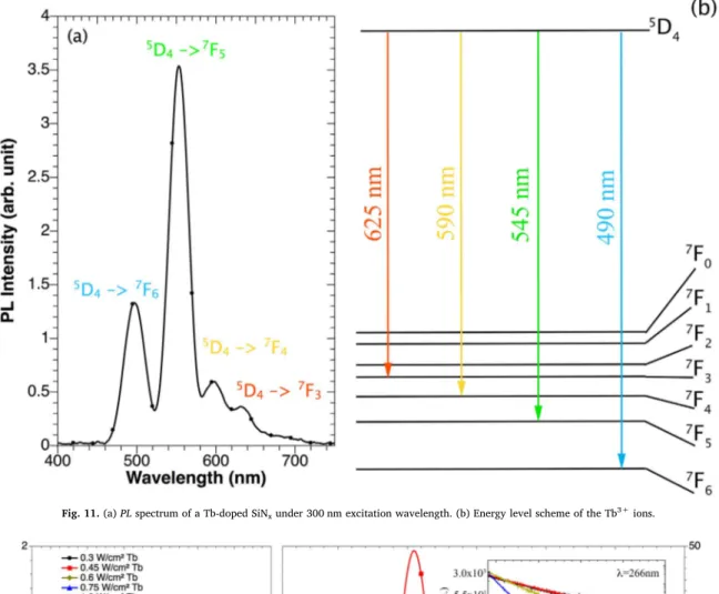
xhost matrix will be investigated through the PL intensity of the Tb3+ions peaks. As shown onFig. 11a, four emission peaks can be observed corresponding to the transitions from the5D
4to the7Filevels as presented onFig. 11b. Note that the emission spectrum has been achieved under a low photon
flux (1.9×10¹⁵
photons/cm2) excitation at 300 nm for the Tb3+ions which has a low absorption cross section below 2×10–21cm2 as reported in [27,46]. Such a result evidences an efficient indirect excitation of Tb3+ ions which may witness a sensitization of the Tb3+ions by defect states of the matrix. Such an excitation process has already been evidenced in Tb3+-doped SiO
xNy and Tb-SixOy systems[23,24].
The influence of the Tb incorporation on the emission properties of the SiNx:Tb3+ layer is presented inFig. 12in which the PL spectra recorded in the 330–720 nm range are reported for different RF power densities applied on the Tb target. The left part of the scale is related to the emission of the host matrix, ranging between 360 and 460 nm while the right part of the scale corresponds to the Tb3+ emission in the 460–720 nm range. All the layers have been annealed at 850 °C during one hour under a pure nitrogenflux. The PL of Tb-free SiNxmatrix is also reported onFig. 12showing a weak emission below 490 nm. In Tb-doped matrix, the PL associated to the defect states disappeared (Fig. 12) contrary to what was observed for non-doped matrix (Fig. 9a). This behavior suggests that an energy transfer may occur from the matrix defect states to the Tb3+ ions. In the 460–720 nm range, the increasing power density applied on the Tb target RFPTb favors the emission intensity of the Tb3+ion which reaches its maximum for 0.45 W/cm2 before decreasing and totally disappears for the highest RFPTbapplied (1.8 W/cm2). Since the Tb3+ lifetime (InsetFig. 12) shows a constant value of about 620 µs for RFPTbup to 0.45 W/cm2, the observed increase of the Tb3+emission intensity up to 0.45 W/cm2 can be associated with the increase of optically active Tb3+ions.
Above 0.45 W/cm2, the decrease of intensity with RFP Tb is attributed either to a concentration quenching process due to rare earth ions clustering [48,49] migrate or coupling Tb3+ions with non radiative centers. This later point is confirmed by both the lifetime (inset ofFig. 12) and the FTIR measurements reported onFig. 13. In the former, the terbium lifetime of the5D4-7F5 transition remains constant (around 620μs) up to RFPTb=0.45 W/cm2. Indeed, below such RFP, the Tb3+ions incorporation does not favor the creation of non-radiative de-excitation paths. After the RFPTb reaches values higher than 0.45 W/cm2, the observed decrease of the Tb3+lifetime (from 620μs to 360 μs and 180 μs) is an evidence of the formation of two new kinds of non-radiative de-excitation channels. Thefirst would be defects in the matrix that can trap the photons. The second would be an energy migration process between Tb3+ions that become close enough to transfer energy among themselves and enhances the probability to reach a trap. In the FTIR measurements, the increase of RFPTb favors the overlapping of TOSi-N-LOSi-N bands around 1000 cm−1 as well as the decrease and the shift of the LOSi-Npeak (Fig. 13). Such a feature is the signature of an increasing disorder and thus an increasing number of defects that may be responsible for the observed PL emission quenching and emission decay time decrease. Thus our optimum settings leading to the higher Tb3+PL intensity are 0.45 W/cm2for the Tb target power density with a nitrogen rate of 20% rN2, and a plasma pressure of 3 mTorr.
Once the energy transfer from the host matrix to the Tb3+ions has been proposed, its mechanism is detailed. A photoluminescence excita-tion (PLE) spectrum of the Tb-doped system was measured for a 545 nm detection wavelength (5D4→7F6transition) and displayed inFig. 14. It can be seen that the doped system is mainly excited in the range of 240–290 nm (5.2–4.3 eV) and decreases then to the limit of detect-ability for excitation wavelengths longer than 335 nm (3.7 eV). This energy range may be associated with electronic transitions occurring from (Ecor≡Si-Si≡ σ*) to (=N-,≡Si-Si≡ σ, or Ev). The broad energy distribution of electronic levels at the origin of energy transfer results in a broad PLE band. It is worth mentioning that the Full Width at Half Maximum (FWHM) of the PLE band is much broader than the FWHM of typical f-d absorption bands of rare earth ions, which is another evidence for indirect excitation of these ions.
Fig. 10. Energy level diagram of the SiNxmatrix with the energy level transitions
observed in the literature[42–46]and the energy transfers possible and observed on
Fig. 14also shows that the Tb3+ions, due to their discrete energy structure, are excited mostly in their high energy levels such as the 4 f75d energy band and the 5H6,7,8 and 5H6,7,8 energy levels. This excitation occurs via energy transfer originating from the electronic transition from (Ecor≡Si-Si≡ σ*) to (=N-, ≡Si-Si≡ σ, or Ev). The Tb3+ ions then undergo non-radiative de-excitation till reaching the 5D
4energy level from which the four characteristic radiative transitions (5D
4→7Fxwith x=3, 4, 5, and 6) take place.
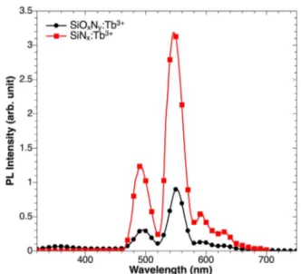
3.3. Comparison of the SiNx:Tb3+and SiOxNy:Tb3+systems
The optimized Tb3+-doped SiNxlayer obtained is compared to an
optimized Tb3+-doped layer made with a silicon oxynitride matrix, SiOxNypreviously studied in our team[25]. The Tb3+ions PL peaks at 285 nm excitation wavelength of our optimized sample is found to be 2.3 times more intense than the optimized sample obtained on the SiOxNy:Tb3+system (Fig. 15). However, considering an application to Si-SCs, the main parameter is not the light that is extracted toward the air but the light extracted toward the substrate, i.e. the SC. As such value is difficult to access experimentally, we calculated it based on ETMM method detailed in Material and methods part (§2) and on experimental PL data recorded in the air.
It has been shown[50]that the Tb3+PL intensity in the air, IPL air, is given by:
Fig. 11. (a) PL spectrum of a Tb-doped SiNxunder 300 nm excitation wavelength. (b) Energy level scheme of the Tb3+ions.
Fig. 12. PL measurements of the host matrix in the 330–460 nm range (Left scale) and of the Tb emission in the 460–740 nm range (Right scale) of undoped and Tb-doped SiNxlayers. The
PL measurements have been carried out using a grating of 1200 s/mm-300 blaze wavelength (bw) and an excitation wavelength of 266 nm. In inset, the Tb3+lifetime for various RFP Tb
I CN V τ
= *. ,
airPL
rad (4)
with C an experimental constant, V being the volume on which the PL excitation is applied, N*being the excited state population density, and τradbeing the Tb3+radiative lifetime. In our experiment, the volume of interaction (77.10−6mm3) and the pump power densityΦ (1.9×10¹⁵ photons/cm2) are constant. Assuming a constantτrad(around 620μs in both matrices) and a low pump power density approximation, we can express the excited state population density as:
N* =KσΦτradNtot (5)
With K an experimental constant, Ntotthe total population density of Tb3+ions, andσ the effective excitation cross-section.
Thus the ratio of the PL intensities in the air can be written as (from Eqs.(4) and (5)): I SiN I SiO N N SiN N SiO N σ SiN σ SiO N ( ) ( ) = ( ) ( ). ( ) ( ) = 2.3 air PL x airPL x y tot x tot x y air x air x y (6)
RBS measurements on both layers are reported in the table as shown elsewhere[26,47].
Thus, the ratio of total population densities is:
N SiN N SiO N ( ) ( ) = 1.8 tot x tot x y (7)
The effective excitation cross-section in the air that represents the mechanisms of absorption and energy transfer between the matrix and the Tb3+ions in the layer as well as the extraction of the Tb3+emission (at 501 nm and 557 nm) from this layer to the air. The ratio of such effective excitation cross-section of the SiNxmatrix over the SiOxNyone can thus be given by:
σ SiN σ SiO N I SiN N SiO N I SiO N N SiN ( ) ( ) = ( ). ( ) ( ). ( ) = 1.3 air x air x y air PL x tot x y airPL x y tot x (8)
The ETMM program yields the integrated luminescence efficiencies ηlumin the layer, in the air, and in the substrate. They are given in
Table 2. We can see that the SiNx layer transfers more to the SC (modeled here by the Si) than the SiOxNylayer.
The ratio of the effective excitation cross-section in the air (Eq.(8)) represents the DS efficiency with extraction in the air. However for silicon solar cell applications, we may be interested in the DS efficiency with extraction in the silicon SC. In order to evaluate this DS efficiency with extraction in silicon, we use the Eqs.(3) and (8)and the integrated luminescence efficiencies ofTable 2to obtain the ratio of the effective
excitation cross-section in the layer and in the substrate (Si-SC):
σ SiN σ SiO N η η σ SiN η η σ SiO N ( ) ( )= / . ( ) / . ( ) i x i x y i lum air lum air x i lum air lum air x y (9)
This equation leads to a ratio of effective excitation cross-section of the SiNxmatrix over the SiOxNyone of 1.9 calculated in the layer and of
Fig. 13. FTIR spectra at Brewster angle of the Tb-doped SiNxlayers for different Tb target
RF power densities.
Fig. 14. PLE spectrum of the SiNx:Tb3+film for a detection wavelength of 545 nm and
energy level diagram of the Tb3+ion with the energy transfer from the matrix in blue and
violet arrows, the non-radiative de-excitation in black straight dashed line arrows, and the radiative de-excitation in colored arrows. (For interpretation of the references to color in thisfigure legend, the reader is referred to the web version of this article).
Fig. 15. Photoluminescence spectra of the optimized samples obtained of Tb3+-doped
SiOxNyand SiNxdoped terbium matrices for a 285 nm excitation wavelength measured
with the 600 lines/mm-750 bw grating.
Table 1
Composition of the Tb-doped SiNxand SiOxNymatrixes[24,47].
Samples Si at% N at% Tb at% O at%
SiNx: Tb3+ 42 56 1.5 _
2.7 calculated in the substrate (Si-SC).
This ratio shows the improvement of the DS efficiency of the SiNx layer compared to the thicker SiNxOyone in the silicon. Part of this difference may be attributed to different thicknesses (225 nm and 93 nm) and different refractive indexes (1.65 and 2.02) for the SiOxNy:Tb3+and SiNx:Tb3+respectively. For the conditions of thick-ness and refractive index employed in this work, the silicon, and thus the silicon solar cells, would receive 5 times more light at 501 nm and 557 nm from the Tb3+-doped SiN
xlayer compared to the SiNxOyone. Thus the increase in the PL intensity is due to two contributions: on one hand to the increase in the Tb3+ions incorporation in the SiNxmatrix
without formation of clusters, and on the other hand to the improve-ment of the conversion efficiency of the layer.
3.4. Device test
The Si-based nitride layers described above have been deposited on top of industrial crystalline Si solar cells. For this purpose, its deposition step has been integrated in the industrial cells fabrication process.
Fig. 16describes schematically the steps followed that corresponds to the standard procedure of the Si-PV industry[51]with the integration of the deposition of our layer. A 200 µm-thick monocrystalline p-type Si wafer is chemically cleaned and textured using a KOH etching prior to operate a n-type doping via a POCL3diffusion at 850 °C during 30 min. Afterwards, an isolation etching process is performed for removing the n-type Si at the edges and backsides. Thereafter a classical removed native oxide procedure is applied using a HF acid. Subsequently a 80 nm-thick Si-based nitride layer is then deposited by means of RF magnetron sputtering using the optimized fabrication conditions de-scribed above, before a post annealing treatment at 850 °C during 5 min to favor the recovering of non-radiative traps. The annealing time has been intentionally fixed at 5 min to avoid any damaging of the p-n junction through diffusion of the dopant. Then the last step of the process consists in screen-printing of Ag-front contacts and Al-back contacts followed by a co-firing.
A Tb3+-doped and undoped SiN
x layers have been deposited to allow the observation of the rare earth doping effect on the optical properties of the device. Indeed, the standard anti-reflective layers of industrial solar cells are silicon nitride ones very close to our undoped layer. This undoped layer is thus used as a reference to determine the difference of efficiency brought by the deposition of the DS layer on top of the cells.
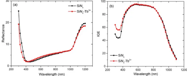
Reflectance measurements have been carried out on the system before depositing the metallic contact (Fig. 17a). This optical char-acteristic plays an important role in a future solar device since our objective consists in optimizing the ARC layer (Anti-Reflective Coat-ing). The Reflectance values for both nitride layers are below the value of 5% in wide domain of wavelength ranging from 350 to 750 nm and a bump is observed after 1020 nm. The reflection efficiency in the 300–1200 nm range is of 6.04% for the device coated with the SiNx ARC layer and reaches 6.20% by adding the rare earth ion. Such value demonstrates the high anti-reflective properties of the couple ARC layer whatever the nitride layer deposited.
The study of the IQE spectra (Fig. 17b) reveals that the Tb3+-doped layer has a higher IQE than the undoped one from 300 to 900 nm with a
Table 2
Integrated luminescence efficiencies of the SiNxand SiOxNymatrixes in the air, the layer,
and the silicon.
ηlum(%) Air Layer Silicon
SiNx 8.7 56.3 35
SiNxOy 13.8 60.2 26
Fig. 16. Scheme of the process fabrication of the solar devices with the developed nitride layers.
Fig. 17. (a) Reflectance characteristics of the SiNx(black) and SiNx:Tb3+(red) anti-reflective layers deposited on a textured Si surface. (b) IQE curves of a solar device with either the
optimized SiNx(black) or the optimized SiNx:Tb3+(red) layers on top. (For interpretation of the references to color in thisfigure legend, the reader is referred to the web version of this
particular increase of 15% in the UV range (300–400 nm). Above 900 nm one can note a slight decrease of the doped-layer with respect to the undoped one. This result shows that the IQE is larger for UV photons thanks to the Tb3+-doped layer. In addition,Fig. 17b display-ing the reflectance of SC topped with our layers (undoped- and Tb3+
-doped-layers) shows that the Tb3+-doped layer has a lower reflectance in the UV range which favors the absorption/or transmission of those photons by the layer/or to the cell. Regarding the IQE spectrum, the Tb3+-doped layer acts as a down-shifting layer that may improve the solar cell efficiency in the UV part of the solar spectrum. This result shows that such DS layer can be a promising solution for improving the Si-SC and that the process developed is fully compatible with the industrial process.
4. Conclusion
In this paper, both layers of SiNxand layers of SiNx:Tb3+deposited by reactive magnetron co-sputtering had been studied in order to obtain a thin down-shifting layer that emits a maximum at 629 nm, 594 nm, 550 nm, and 493 nm (terbium peaks) and is also an anti-reflective layer. Studies of the composition, the microstructure, and the optical properties enabled a better understanding of the requirements for obtaining such a layer. Comparing those studies with photolumines-cence analyses leads to a better understanding of the properties needed to reach a high terbium emission. An optimized layer has been determined for a plasma pressure of 3 mTorr, a nitrogen ratio rN2of 20%, and a 0.45 W/cm2 power density on the terbium target. Such SiNx-based optimized layer was found to transmit 5 times more down shifted light toward the solar cell than a comparable SiOxNy-based layer previously developed. For the monolithic crystalline Si solar cells with down-shifting layer, the IQE of the two optimized layers doped or not were compared. It was found that the down-shifting layer improves by 15% the IQE in the UV part of the solar spectrum. The next step will consist in determining the optical-electrical characteristic of the solar cell with a downshifting layer on the top.
Acknowledgments
This work was financially supported by the French Research National Agency through the GENESE project (N° ANR-13-BS09-0020-01) and the LABEX EMC3 ASAP project. The French authors want to thanks the French ministry for the support through the Partenariat Hubert Curien (PHC) Programs Orchid n° 33572XF and Polonium n°27720WC.
Lucile Dumont thanks CNRS and the Region Basse-Normandie for their PhD student support. In Poland, this work was funded by National Science Centre under Project No. DEC-2012/05/D/ST7/01121.
References
[1] E. Radziemska, The effect of temperature on the power drop in crystalline silicon solar cells, Renew. Energy 28 (2003) 1–12.
[2] E. Radziemska, E. Klugmann, Thermally affected parameters of the current–voltage characteristics of silicon photocell, Energy Convers. Manag. 43 (2002) 1889–1900,
http://dx.doi.org/10.1016/S0196-8904(01)00132-7.
[3] P. Singh, S. Singh, M. Lal, M. Husain, Temperature dependence of I–V character-istics and performance parameters of silicon solar cell, Sol. Energy Mater. Sol. Cells 92 (2008) 1611–1616,http://dx.doi.org/10.1016/j.solmat.2008.07.010. [4] E. Yablonovitch, Statistical ray optics, JOSA 72 (1982) 899–907.
[5] M.A. Green, K. Emery, Y. Hishikawa, W. Warta, E.D. Dunlop, Solar cell efficiency tables (Version 45): solar cell efficiency tables, Progress. Photovolt.: Res. Appl. 23 (2015) 1–9,http://dx.doi.org/10.1002/pip.2573.
[6] J. Zhao, M. Green, et al., Optimized antireflection coatings for high-efficiency silicon solar cells, IEEE Trans. Electron Devices 38 (1991) 1925–1934. [7] M.C. Wei, S.J. Chang, C.Y. Tsia, C.H. Liu, S.C. Chen, SiNxdeposited by in-line
PECVD for multi-crystalline silicon solar cells, Sol. Energy 80 (2006) 215–219,
http://dx.doi.org/10.1016/j.solener.2005.05.015.
[8] C. Strümpel, M. McCann, G. Beaucarne, V. Arkhipov, A. Slaoui, V.Švrček, C. del Cañizo, I. Tobias, Modifying the solar spectrum to enhance silicon solar cell efficiency—An overview of available materials, Sol. Energy Mater. Sol. Cells 91
(2007) 238–249,http://dx.doi.org/10.1016/j.solmat.2006.09.003.
[9] E. Klampaftis, D. Ross, K.R. McIntosh, B.S. Richards, Enhancing the performance of solar cells via luminescent down-shifting of the incident spectrum: a review, Sol. Energy Mater. Sol. Cells 93 (2009) 1182–1194,http://dx.doi.org/10.1016/j.solmat. 2009.02.020.
[10] B.S. Richards, Enhancing the performance of silicon solar cells via the application of passive luminescence conversion layers, Sol. Energy Mater. Sol. Cells 90 (2006) 2329–2337,http://dx.doi.org/10.1016/j.solmat.2006.03.035.
[11] F. Auzel, Upconversion processes in coupled ion systems, J. Lumin. 45 (1990) 341–345,http://dx.doi.org/10.1016/0022-2313(90)90189-I.
[12] A. Shalav, B.S. Richards, M.A. Green, Luminescent layers for enhanced silicon solar cell performance: up-conversion, Sol. Energy Mater. Sol. Cells 91 (2007) 829–842,
http://dx.doi.org/10.1016/j.solmat.2007.02.007.
[13] K.D. Oskam, R.T. Wegh, H. Donker, E.V.D. van Loef, A. Meijerink, Downconversion: a new route to visible quantum cutting, J. Alloy. Compd., 300- 301 (2000) 421–425,
http://dx.doi.org/10.1016/S0925-8388(99)00755-0.
[14] B.S. Richards, Luminescent layers for enhanced silicon solar cell performance: down-conversion, Sol. Energy Mater. Sol. Cells 90 (2006) 1189–1207,http://dx. doi.org/10.1016/j.solmat.2005.07.001.
[15] P. Würfel, Physics of Solar Cells: From Basic Principles to Advanced Concepts, WILEY-VCH, 2009.
[16] K.R. McIntosh, G. Lau, J.N. Cotsell, K. Hanton, D.L. Bätzner, F. Bettiol, B.S. Richards, Increase in external quantum efficiency of encapsulated silicon solar cells from a luminescent down-shifting layer, Progress. Photovolt.: Res. Appl. 17 (2009) 191–197,http://dx.doi.org/10.1002/pip.867.
[17] D. Chen, Y. Wang, Y. Yu, P. Huang, F. Weng, Quantum cutting downconversion by cooperative energy transfer from Ce3+to Yb3+in borate glasses, J. Appl. Phys. 104
(2008) 116105,http://dx.doi.org/10.1063/1.3040005.
[18] Q. Duan, F. Qin, D. Wang, W. Xu, J. Cheng, Z. Zhang, W. Cao, Quantum cutting mechanism in Tb3+-Yb3+co-doped oxyfluoride glass, J. Appl. Phys. 110 (2011)
113503,http://dx.doi.org/10.1063/1.3662916.
[19] X. Liu, S. Ye, Y. Qiao, G. Dong, B. Zhu, D. Chen, G. Lakshminarayana, J. Qiu, Cooperative downconversion and near-infrared luminescence of Tb3+–Yb3+
co-doped lanthanum borogermanate glasses, Appl. Phys. B 96 (2009) 51–55,http://dx. doi.org/10.1007/s00340-009-3478-z.
[20] D. Serrano, A. Braud, J.L. Doualan, W. Bolaños, R. Moncorgé, P. Camy, Two-step quantum cutting efficiency in Pr3+-Yb3+codoped KY
3F10, Phys. Rev. B 88 (2013),
http://dx.doi.org/10.1103/PhysRevB.88.205144.
[21] I.A.A. Terra, L.J. Borrero-González, T.R. Figueredo, J.M.P. Almeida,
A.C. Hernandes, L.A.O. Nunes, O.L. Malta, Down-conversion process in Tb3+–Yb3+
co-doped Calibo glasses, J. Lumin. 132 (2012) 1678–1682,http://dx.doi.org/10. 1016/j.jlumin.2012.02.019.
[22] V.K. Tikhomirov, V.D. Rodríguez, J. Méndez-Ramos, J. del-Castillo, D. Kirilenko, G. Van Tendeloo, V.V. Moshchalkov, Optimizing Er/Yb ratio and content in Er–Yb co-doped glass-ceramics for enhancement of the up- and down-conversion lumi-nescence, Sol. Energy Mater. Sol. Cells 100 (2012) 209–215,http://dx.doi.org/10. 1016/j.solmat.2012.01.019.
[23] Y.-T. An, C. Labbé, M. Morales, P. Marie, F. Gourbilleau, Fabrication and photoluminescence properties of Tb-doped nitrogen-rich silicon nitridefilms, Phys. Status Solidi C. 9 (2012) 2207–2210,http://dx.doi.org/10.1002/pssc.201200253. [24] A. Podhorodecki, L.W. Golacki, G. Zatryb, J. Misiewicz, J. Wang, W. Jadwisienczak, K. Fedus, J. Wojcik, P.R.J. Wilson, P. Mascher, Excitation mechanism and thermal emission quenching of Tb ions in silicon rich silicon oxide thinfilms grown by plasma-enhanced chemical vapour deposition—Do we need silicon nanoclusters? J. Appl. Phys. 115 (2014) 143510,http://dx.doi.org/10.1063/1.4871015. [25] C. Labbé, Y.-T. An, G. Zatryb, X. Portier, A. Podhorodecki, P. Marie, C. Frilay,
J. Cardin, F. Gourbilleau, Structural and emission properties of Tb3+-doped
nitrogen-rich silicon oxynitridefilms, Nanotechnology 28 (2017) 115710 (p. 14),
http://dx.doi.org/10.1088/1361-6528/aa5ca0.
[26] L. Dumont, J. Cardin, P. Benzo, M. Carrada, C. Labbé, A.L. Richard, D.C. Ingram, W.M. Jadwisienczak, F. Gourbilleau, SiNx:Tb3+–Yb3+, an efficient
down-conver-sion layer compatible with a silicon solar cell process, Sol. Energy Mater. Sol. Cells 145 (2016) 84–92,http://dx.doi.org/10.1016/j.solmat.2015.09.031.
[27] D.K. Sardar, K.L. Nash, R.M. Yow, J.B. Gruber, U.V. Valiev, E.P. Kokanyan, Absorption intensities and emission cross sections of Tb3+(4f8) in TbAlO
3, J. Appl.
Phys. 100 (2006) 83108,http://dx.doi.org/10.1063/1.2358401.
[28] O. Debieu, R.P. Nalini, J. Cardin, X. Portier, J. Perrière, F. Gourbilleau, Structural and optical characterization of pure Si-rich nitride thinfilms, Nanoscale Res. Lett. 8 (2013) 1–13,http://dx.doi.org/10.1186/1556-276X-8-31.
[29] A.R. Forouhi, I. Bloomer, Optical dispersion relations for amorphous semiconduc-tors and amorphous dielectrics, Phys. Rev. B 34 (1986) 7018–7026,http://dx.doi. org/10.1103/PhysRevB.34.7018.
[30] P. Yeh, Optical Waves in Layered Media, Wiley, New York, 1988.
[31] ASTM G173-03 (2012), Standard Tables for Reference Solar Spectral Irradiances: Direct Normal and Hemispherical on 37° Tilted Surface, ASTM International, West Conshohocken, PA, 2012,〈www.astm.org〉.
[32] H. Benisty, R. Stanley, M. Mayer, Method of source terms for dipole emission modification in modes of arbitrary planar structures, JOSA A 15 (1998) 1192–1201. [33] J.-P. Weber, S. Wang, A new method for the calculation of the emission spectrum of DFB and DBR lasers, IEEE J. Quantum Electron. 27 (1991) 2256,http://dx.doi.org/ 10.1109/3.97269.
[34] Y.G. Boucher, Theoretical investigation of amplified spontaneous emission in an active structure by extended (3×3) transfer matrix formalism: the case of a non-uniform longitudinal distribution of emitters, J. Eur. Opt. Soc. - Rapid Publ. 1 (2006),http://dx.doi.org/10.2971/jeos.2006.06027.
hydrogenated amorphous silicon nitride thinfilms, Appl. Phys. Lett. 73 (1998) 3866,http://dx.doi.org/10.1063/1.122919.
[36] L. Huang, K.W. Hipps, J.T. Dickinson, U. Mazur, X.D. Wang, Structure and composition studies for silicon nitride thinfilms deposited by single ion bean sputter deposition, Thin Solid Films 299 (1997) 104–109,http://dx.doi.org/10. 1016/S0040-6090(96)09446-1.
[37] S. Hasegawa, L. He, Y. Amano, T. Inokuma, Analysis of SiH and SiN vibrational absorption in amorphous SiNx:Hfilms in terms of a charge-transfer model, Phys.
Rev. B 48 (1993) 5315–5325,http://dx.doi.org/10.1103/PhysRevB.48.5315. [38] W.R. Knolle, Correlation of refractive index and silicon content of silicon oxinitride
films, Thin Solid Films 168 (1989) 123–132, http://dx.doi.org/10.1016/0040-6090(89)90695-0.
[39] J.G.E. Gardeniers, H.A.C. Tilmans, C.C.G. Visser, LPCVD silicon-rich nitridefilms for applications in micromechanics, studied with statistical experimental design, J. Vac. Sci. Technol. A 14 (1996) 2879–2892,http://dx.doi.org/10.1116/1.580239. [40] M. Wang, M. Xie, L. Ferraioli, Z. Yuan, D. Li, D. Yang, L. Pavesi, Light emission
properties and mechanism of low-temperature prepared amorphous SiNxfilms. I.
Room-temperature band tail states photoluminescence, J. Appl. Phys. 104 (2008) 83504,http://dx.doi.org/10.1063/1.2996292.
[41] J. Kistner, X. Chen, Y. Weng, H.P. Strunk, M.B. Schubert, J.H. Werner, Photoluminescence from silicon nitride—no quantum effect, J. Appl. Phys. 110 (2011) 23520,http://dx.doi.org/10.1063/1.3607975.
[42] S.V. Deshpande, E. Gulari, S.W. Brown, S.C. Rand, Optical properties of silicon nitridefilms deposited by hot filament chemical vapor deposition, J. Appl. Phys. 77 (1995) 6534–6541,http://dx.doi.org/10.1063/1.359062.
[43] C. Mo, L. Zhang, C. Xie, T. Wang, Luminescence of nanometer‐sized amorphous silicon nitride solids, J. Appl. Phys. 73 (1993) 5185–5188,http://dx.doi.org/10.
1063/1.353796.
[44] J. Robertson, M.J. Powell, Gap states in silicon nitride, Appl. Phys. Lett. 44 (1984) 415–417,http://dx.doi.org/10.1063/1.94794.
[45] W.L. Warren, J. Kanicki, J. Robertson, P.M. Lenahan, Energy level of the nitrogen dangling bond in amorphous silicon nitride, Appl. Phys. Lett. 59 (1991) 1699–1701,
http://dx.doi.org/10.1063/1.106222.
[46] L. Zhang, H. Jin, W. Yang, Z. Xie, H. Miao, L. An, Optical properties of single-crystallineα-Si3N4nanobelts, Appl. Phys. Lett. 86 (2005) 61908,http://dx.doi.org/
10.1063/1.1862753.
[47] Y.-T. An, C. Labbé, J. Cardin, M. Morales, F. Gourbilleau, Highly efficient infrared quantum cutting in Tb3+- Yb3+codoped silicon oxynitride for solar cell
applica-tions, Adv. Opt. Mater. 1 (2013) 855–862,http://dx.doi.org/10.1002/adom. 201300186.
[48] D. Umamaheswari, B.C. Jamalaiah, T. Sasikala, T. Chengaiah, I.-G. Kim, L. Rama Moorthy, Photoluminescence and decay behavior of Tb3+ions in sodium
fluoro-borate glasses for display devices, J. Lumin. 132 (2012) 1166–1170,http:// dx.doi.org/10.1016/j.jlumin.2011.12.080.
[49] F. Benz, J.A. Guerra, Y. Weng, A.R. Zanatta, R. Weingärtner, H.P. Strunk, Concentration quenching of the green photoluminescence from terbium ions embedded in AlN and SiC matrices, J. Lumin. 137 (2013) 73–76,http://dx.doi.org/ 10.1016/j.jlumin.2012.12.028.
[50] D. Navarro-Urrios, Y. Lebour, O. Jambois, B. Garrido, A. Pitanti, N. Daldosso, L. Pavesi, J. Cardin, K. Hijazi, L. Khomenkova, F. Gourbilleau, R. Rizk, Optically active Er3+ions in SiO
2codoped with Si nanoclusters, J. Appl. Phys. 106 (2009)
93107,http://dx.doi.org/10.1063/1.3253753.
[51] D.-H. Neuhaus, A. Münzer, Industrial silicon wafer solar cells, Adv. Optoelectron. (2007) 1–15,http://dx.doi.org/10.1155/2007/24521.


![Fig. 10. Energy level diagram of the SiN x matrix with the energy level transitions observed in the literature [42–46] and the energy transfers possible and observed on Fig](https://thumb-eu.123doks.com/thumbv2/123doknet/13752362.437825/9.892.78.410.80.468/energy-diagram-transitions-observed-literature-transfers-possible-observed.webp)