332 pp. 332-343
An open software-radio architecture supporting
advanced 3G+ systems
Christian BONNET*, Giuseppe CAIRE*, Alain ENOUT*, 1, Pierre A. HUMBLET*, Giuseppe MONTALBANO*, 2, Alessandro NORDIO*, and Dominique NUSSBAUM*, 3,
Thomas HOHNE**, 4, Raymond KNOPP**, 5 and Bixio RIMOLDI**
Abstract
This paper describes a software-radio architecture developed for providing real-time wide-band radio commu- nication capabilities in a form attractive for advanced 3G systems research. It is currently being used to implement signaling methods and protocols similar, but not limited to, evolving 3G radio standards (e.g. UMTS, CDMA2000). An overview of the hardware system is provided along with example software implementations on both high-perfo- mance DSP systems and conventional microprocessors.
Key words : Mobile radiocommunication, Digital signal proces- sing, Radio interface, Test facility, Software radio, System architecture, Transmitter, Receiver, UMTS.
UNE PLATEFORME RADIO LOGICIELLE OUVERTE POUR LES SYSTI~MES 3G+ R6sum6
Cet article ddcrit une plate-forme radio logicielle reconfigurable, permettant de rdaliser d'une manibre souple des traitements en temps rdel sur une interface radio de type ~G. Cette plate-forme est actuellement uti- lisde pour implementer des mdthodes de transmission-rdception ainsi que des protocoles, inspirds des normes 3G (UMTS, CDMA2000). Une vue d'ensemble de l'architecture matdrielle est donnde dans cet article ainsi que des exemples d'implantations logicielles, aussi bien sur processeurs de traitement du signal (DSP) que sur des processeurs classiques.
Mots cl6s: Radiocommunication service mobile, Traitement num6rique signal, Interface radio, Radio logicielle, Installation essai, Architecture syst~me, Emetteur, R6cepteur, UMTS.
Contents
I. Introduction and motivation II. System architecture
III. Digital signal processing
IV. Validation of the existing platform V. Conclusion
References (22 ref )
I. INTRODUCTION AND MOTIVATION
The presence of several different wireless communi- cation standards and the wide variety of services provided by mobile communication operators has created the pro- blem of providing universal seamless connection to custo- mers with different service requirements at any point on the globe. Software Radio is an enabling technology for systems aiming at handling several different standards and different services and thus represents a solution to this problem. Generally, Software Radio is a very broad term encompassing several levels in the protocol stack (see e.g. [1, 2, 3] and references therein). Motivated by the worldwide activity around third generation (3G) mobile communication systems, Eurrcom and Er'~ have launched a joint project whose objective is to design and implement a real-time software radio communication platform to validate advanced mobile communication signal processing algorithms. The right to transmit has been granted for one 5 MHz UMTS channel in both France and Switzerland for experimental purposes.
The platform is characterized by the following major features:
*Institut Eurrcom (Eurecom's research is partially supported by its industrial partners: Ascom, Bouygues Telecom, Crgrtel, France Trl6com, Hitachi, Motorola, STMicroelectronics, Swisscom, Texas Instruments, and Thomson CSF) - B.P. 193, 06904 Sophia-Antipolis CEDEX, France - Tel: +33 493002904, Fax: +33 493002627 - E-mail: [email protected].
** Mobile Communications Laboratory (LCM - LCM was funded in part by Nokia/DiAx/sBc) - Swiss Federal Institute of Technology - 1015 Lau- sanne, Switzerland Tel: +41 2 1 6 9 3 2 6 7 9 - Email: [email protected] April 12, 2001.
1. A. Enout is now with UDcast, Sophia Antipolis, France.
2. G. Montalbano is now with Philips Semiconductors, Sophia Antipolis, France. 3. The authors appear in alphabetical order.
4. T. H6hne is now with the Nokia Research Center, Helsinki, Finland. 5. R. Knopp is now with Institut Eur6com.
C. BONNET -- AN OPEN SOFtWARE-RADIO ARCHITECTURE SUPPORTING ADVANCED 3 G + SYSTEMS
9 Flexibility, achievable by a software driven system. 9 Duplex communication.
9 Multiple antennas transmit and receive signal pro- cessing (i.e. joint spatio-temporal signal processing).
Flexibility remains a key word for a software-defi- ned system. In our case it serves several purposes. For instance one may perform propagation channel measu- rements and transmitter characterization, evaluate the performance of different signal processing algorithms for both single user and multi-user systems under dif- ferent operating conditions. Duplex communication is
also necessary to allow higher-layer protocol testing and services, and to analyze more complex system aspects, such as multiple-access, power control, and optimize down-link signal processing from up-link measurements. In a second phase, the platform will allow Multiple-antenna signal processing, or more generally, spatio-temporal signal processing (also known as array processing) since this a very promising ensemble of techniques able to significantly increase the capacity of wireless communication systems.
The main focus of this paper is on the description of the basic platform architecture and signal processing to implement the essential physical layer level procedures of the UMTS standard operating in Time Division Duplex
( U M T S / T D D ) mode.
At the physical layer level, Software Radio gene- rally requires the development of signal processing algorithms suited to implementation on a general pur- pose programmable processor (as opposed to analog or digital dedicated hardware). For this reason the posi- tion of Analog to Digital (A/D) and Digital to Analog (D/A) conversion must be moved as close as possible to the antennas. The goal is to perform operations like
channel selection [4, 5], synchronization and detection in the all-digital domain, by using high performance Digital Signal Processors (DSPS). Special care must be dedicated to the transmission and reception front-end architecture. In fact, this should be independent on sys- tem-dependent parameters like the signal bandwidth and the symbol (or chip, in a CDMA system) rate. When designing software radio algorithms it is assumed that a multi-band Radio Frequency (RF) section takes care of translating the desired signal from a fixed Interme- diate Frequency (IF) carrier to the required R~ carrier in the transmitter, and vice-versa in the receiver. Then we are concerned with the efficient generation of an 1F analog signal from a baseband digital signal (transmit- ter front-end) and with the reverse operation (receiver front-end). Once the end-to-end transmitter receiver architecture is defined the next step consists in syn- chronizing the receiver, estimating the channels asso- ciated with the users, and eventually detecting the transmitted symbols. All these operations are perfor- med in real-time on our platform.
The adopted modulation scheme (BPSK and QPSK), the spread signal bandwidth (5 MHz), the spreading gain (DS-CDMA with allowed spreading gain of 1, 2, 4, 8, 16) and the frequency band (around 2.1 GHz) are the same as
333 those defined in the UMTS/TDD specifications. The TDD mode has been chosen because under certain circums- tances it allows the exploitation of the channel recipro- city between up-link and down-link in duplex communication, and also reduces the DSP computational load for a given bandwidth.
The solutions proposed in this paper can also be applied to a wide class of linearly-modulated digital signals (including most of today's and future mobile communications standards, like GSM, IS-54, IS-136, ~S-95, and DECT (see e.g. [6] and references therein), UMTS (both FDO and TOO modes) [71, CDMA2000 (see e.g. [8, 9]) and EDGE (see e.g. [10] and references therein).
II. S Y S T E M A R C H I T E C T U R E
In a first phase, the development of the platform has been based on a single antenna architecture for the Mobile Terminal (MT) as well as for the Base Station (BTS). The retained architecture permits to easily enhance the capabilities of the platform without redesigning the essential hardware and software parts.
The BTS and the MT are based on the same hardware platform and differ only in the software implementation. The different hardware parts of the platform are highly partitioned in order to enable the use of as many standard cards and components as possible.
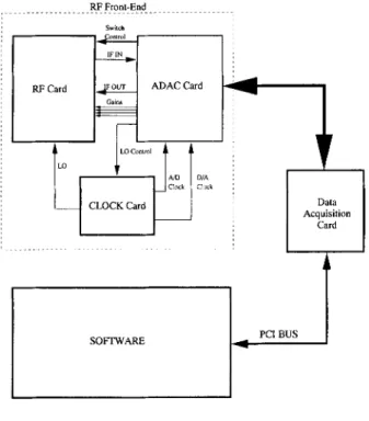
The hardware portion of the test-bed consists of 4 elements which are under software control, namely
1. a pct bus based reconfigurable data acquisition card
(DAQ)
based on a Field Programmable Gate Array (FPGA)2. an RF front-end
9 a single stage up/down-conversion from/to a 70 MHz intermediate frequency (IF) carrier with
time-division-duplex (TDD)
multiplexing9 1 high-speed 12-bit bandpass sampling A/D converter (fADC = 14.7456 MHz)
9 1 high-speed 12-bit up-sampling D/A converter
(fDAC = 8 X fADC = 117.9648 MHz)
9 8 slow D/A converters for controlling various amplifier gains on the RF card
9 control for various switches on RF card
3. a clock card for generating sampling clocks (fixed frequency) and local oscillators (programmable frequency)
We show a simplified block diagram of the entire sys- tem for a single antenna in Figure 1.
We have considered two software implementations, the first using a combination of commercially available embedded DSP cards and a common PC and the second using the DSP units (e.g. MMX) of a standard PC under an operating system proving hard real-time support (e.g. RTLinux). Both run in real-time and are compatible over the air.
334 C. BONNET - AN OPEN SOFTWARE-RADIO ARCHITECTURE SUPPORTING ADVANCED 3G+ SYSTEMS
RF Front-End Switch
RF Card ADAC Card :~..~1
SOFTWARE PCIBUS
FIG. l . - - System Architecture.
Architecture systkme.
Data Acquisition
Card
T
tunable gain control and directly sampled at 14.7456 MSamp/s The samples are transferred via a rib- bon cable using high-speed line drivers to the
data acqui-
sition unit
(DAQ). The mode of the transceiver (i.e. transmission, reception, calibration) is fully control- lable from the software portion of the platform.On the transmission end (Tx), samples from the DAQ arrive at a rate of 14.7456 MSamp/s and drive a hard- ware up-sampling circuit and a high-speed D/A conver- ter (117.9648 MSamp/s) to directly synthesize the 70 MHz IF signal. This procedure is described in more detail in 11.1.2. This signal is then amplified, up-conver- ted to RE, filtered and amplified by a variable-gain power amplifier.
Special low-speed lines control the gains of the Rx variable-gain amplifier and Tx Power Amplifier, LO fre- quency, as well as the antenna switch. Although not included in Figure 2, automatic wide-band calibration capabilities (for both Tx and Rx) are included in the design, which are required for multiantenna systems (see e.g. [11]). These will be used in a later stage of the pro- ject where the architecture will be extended to implement multiple antenna transceivers. The basic characteristics of the RF frontend are summarized in Table I.
II.1. RV Front-end
A simplified block diagram of our RF front-end is shown in Figure 2. It was designed in conjunction with STMicroelectronics in Geneva, Switzerland. On recep- tion (Rx), the RF signal is filtered, amplified and down-converted to a 70 MHz intermediate frequency (IF). The local oscillator frequency is digitally tunable in steps of 500 Hz. The IF signal is amplified by a digitally
II.1.1. P a s s b a n d MD C o n v e r s i o n
Once the RF signal at the antenna has been down-converted to IF, it is sampled by an A/D converter at a certain
ratefAoc (figure
9). CallingriF(t )
the received IF analog signal and choosingfaoc > 2W
according to [4], because of the periodicity of the discrete-time signal spectrum, the resulting real sampled signalr[n] = rlF(n/fAoc)
is pass-band with a spectrum replica centered atfADC/4
(although fm andfADC
at the receiver can be different from flF andfAOC
at the transmitter, for simplicity we use the same notation).70MHz
To Antenna~
~ )'~ <
C • •
12-bit
samples
@ 16.74
MHz
AGC-Level
LO Frequency Control
~ ~Output Power Control
70 MHz
TxJRx Switch
FIG. 2 . - - RE Front-end.
Tdte RF.
C. BONNET -- AN OPEN SOFTWARE-RADIO ARCHITECTURE SUPPORTING ADVANCED 3G+ SYSTEMS TABLE I. - - RF Front-end Characteristics.
Les caractdristiques de la t~te radiofrgquence.
Frequency B a n d 2100-2170 MHz Bandwidth 5 MHz (initially) Transmit Power 1 W (per antenna) Receiver Sensitivity -100 dBm Noise Figure < 5 dB Input IP3 > -7 dBmDuplex mode Time Division
Rx Gain Control digital tuning, 1 dB steps over 40 dB Tx Power Control digital tuning, 1 dB steps over 80 dB range Local Oscillator digital tuning, steps of a few kHz
in each band
l~F Calibration digital control, Tx and Rx Direct IF sampling 12-bit A/D @ 14.7456 MSamp/s (70 MHz) on Rx
Direct IF sampling 12-bit D/A @ 117.9648 MSamp/s (70 MHz) on Tx
Digital Interface High speed: Low-Voltage Differential Signaling (LVDS)
Low speed: 3.3V CMOS line drivers
Notice that here in order to avoid signal re-sampling we suppose the rate
fADC
to be a multiple integer of the chip rate (i.e.fADC
= Ncfc where in our implementation we set N c = 4).Although a base-band version of the received signal can be obtained by multiplying
r[n]
by (_j)n and then by low pass filtering, we will show further how the channel estimation and the data detection processes can be per- formed at pass-band.11.1.2. Passband D]A Conversion
D/A converters have an impulse response PDAC (t) that can be approximated as a rectangular pulse of duration
1/foa c
with frequency response o f the form ofsinc(f/fDac ).
If the discrete-time input of the D/A conver-ter is the pass-band signal
x'[n],
then the spectrum of the output signal is given by(1)
YQ') = ~ X'O c- ifDac)Sinc~/fDac )
i
where )('09 is the discrete-time Fourier transform o f
x'[n],
defined byX'OC) = Z x'[nleJ2nnflfDAC
n
Hence, the spectrum replica located at f r e q u e n c y
flF
is attenuated and distorted by the D/A impulse res- ponse as shown in figure 8(a). A w a y to r e d u c e the attenuation consists o f using a D/A converter working at ratefa = LD/AfDAC,
whereLD/z
is a suitable integer, and up-samplingx'[n]
by the factorLD/A.
By choosingLD/A
such that fa>>flF,
the spectrum replica aroundflF
falls inside the first lobe of the D/A frequency res-335 p o n s e since its first zero is located at
fe
(see figure 8(b)). M o r e o v e r it is possible to c o m p e n s a t e in part the distortion o f the D/A converter by i n t r o d u c i n g a p a s s - b a n d FIR filter between the u p - s a m p l e r and the D/A converter. The filter must be designed in order to enhance the spectrum replica at IF while attenuating the other replicas.Low complexity implementation. Denote by
x"[n]
the up-sampled version ofx'[n],
given by(2)
x"[n]={O [k]
otherwisef~176and by
hD/a[n ]
the filter impulse response. The filter out- put is given by(3) x ' [ n ] = 2
hDIA[m]x"[N-M]
m
If the filter impulse response has length
Lo/A,
there is only a single non-zero term in the sum in the right hand side o f the above equation. Then, x"'[n] =hD/a[m]x'[k]
where k =[n/LD/A]
and m = n moduloLD/A.
Therefore, the computational cost of the filtering opera- tion consists o f one real product per output sample at rate
fa"
After the D/A conversion, the continuous-time signaly(t)
is eventually up-converted to the RF carrier and sent to the antenna.II.2. Data Acquisition Card
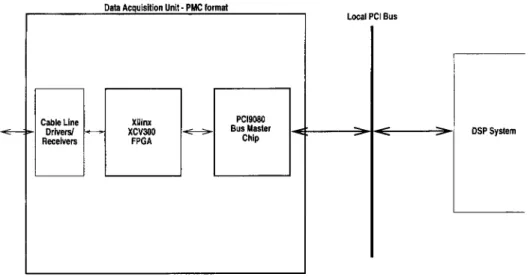
The data acquisition card is a PCI bus-mastering device permitting high-speed full duplex parallel trans- fer of digital data from an external device. It contains the necessary glue logic which connects the input (A/D) and output (D/A) sample streams as well as some control signals to the main CPU/DSP. A PCt architecture was adopted since it is the most general purpose bus archi- tecture and is used on most standard Pcs, as well as DSP systems. It consists o f two components, namely a powerful Xilinx Field Programmable Gate Array (FPGA) XCV300 [12] and a bus-mastering PCI controller PLX9080 [13]. The format is a
ecI Mezzanine Card
(PMC) to allow for integration into both embedded DSP architectures and ordinary PCS. A simplified overview of the DAQ is shown in Figure 3.Firmware on the FPGA for formatting and transfer- ring data via the DMA engines of the PLX9080 to the host (DSP, CPU) m e m o r y has been developed in VIaDL
(Very
High Speed Integrated Circuit Hardware Description
Language).
After an initial configuration phase, trans-fers are continuous and completely transparent to the host, who just "sees" a circular buffer containing samples acquired from or to be transferred to the exter- nal RF front-end.
The basic components of the DAQ are the following 1. Line Drivers/Receivers for transfer from external
devices via ribbon-cables
336 c. BONNET - AN OPEN SOFTWARE-RADIO ARCHITECTURE SUPPORTING ADVANCED 3G+ SYSTEMS
Data Acquisition Unit - PMC format
Cable Line Xilinx PCI9080 Drivers/ ! ~ XCV300 ~ Bus Master Receivers FPGA Chip
Local PCI Bus
: - - - ~ DSP System
FIG. 3. - - Data Acquisition Unit.
Unit~ d'acquisition de donnges.
2. A reconfigurable FPGA-based 16-bit bi-directional interface external device (up to 30 Msamp/s full-duplex)
3. A PCI bus-mastering controller for direct transfer of samples to/from memory (DMA) on PClbased signal processing units (e.g. DSP cards, high-performance PCS, workstations (SPARC, PowerPc, Alpha), embed- ded processor cards, etc.)
4. A Processor Mezzanine Card (PMC) form-factor for
maximum flexibility
The FPGA is p r o g r a m m e d via the PCI bus by serial download.
PR{MARY PCI BUS
I I . 3 . T e x a s I n s t r u m e n t s TMSC6201 I m p l e m e n t a t i o n
The embedded DSP architecture is based on a com- mercially available dual-DsP card (Spectrum Signal Pro- cessing Daytona [21]. The basic architecture is shown in Figure 4 and is centered around 2 Texas Instruments TMSC6201 fixed-point DSPS. These DSPS are capable o f providing a m a x i m u m o f 1600 M1PS each. Our DAQ is placed on the local PCI bus o f the DSP board and trans- fers samples to/from both of the m e m o r y buffers on the DSPS busses. These buffers are used as temporary sto- rage as the internal (fast) m e m o r y of the DSP is rather small. The DSP DMA engines take care o f automatically transferring data to their internal m e m o r y concurrently with the signal processing functions. One DSP is used exclusively for transmission functions and the other for reception.
The DSPs are used for the front-end processing as des- cribed in the previous sections. Symbol rate data is trans- ferred via the pcI bus to the PC which hosts the DSP card. This data is processed by the Pentium and handles tasks
PENTIUM PC
FIG. 4. - - Embedded DSP Architecture.
Architecture DSP int~gr(e.
such as Viterbi decoding, carrier frequency offset com- pensation, higher layer protocol stacks, etc.
I I . 4 . R T L i n u x - b a s e d P c I m p l e m e n t a t i o n
The second implementation does not rely on embed- ded DSPS. Here the DAQ is placed on the master PCI bus of a workstation, possibly multiprocessor, running the hard
C. BONNET -- AN OPEN SOFTWARE-RADIO ARCHITECTURE SUPPORTING ADVANCED 3 G + SYSTEMS
real-time extension to the Linux operating system, RTLi- nux[22]. The software radio runs in kernel space and is integrated into the tPV4 (Internet Protocol) subsystem of Linux as a network device.
This x86 implementation makes use of the MMX (multimedia extensions) SIMD (single instruction multiple data) instructions for obtaining maximum processor effi- ciency for intensive DSP computations. All DSP routines use fixed-point arithmetic and are written in C with embedded assembly macros for time-critical code sec- tions. We typically make use of
1. MMX packed 16-bit arithmetic (multiply, add, MAC, interleaving, etc.)
2. loop unrolling 3. software pipelining
Because of the high-level software structure, this should be portable to other process or architectures (e.g. PowerPc, Alpha, etc.). For the same reason, it is easily portable to large-scale SMP (symmetric multi-pro- cessing) platforms which couid be useful for advanced base-station implementations.
337 UMTS-TDD 3GPP standard [14] and are now implementing a complete subset of layers 1 and 2 of the true standard (including 1.28 MChips/s version). The main difference of the current implementation is that the hardware por- tion provides a clock yielding a symbol (chip) rate of 3.6864 Msymbols/s and not 3.84 Msymbotl/s.
3.1. Frame/Slot structure
The frame structure of this TDD implementation is shown in Figure 5. We see that each frame is composed of 15 slots which can be arbitrarily distributed between up-link and downlink streams. The first slot in every frame contains the synchronization sequence and is by default a downlink slot. The synchronization sequence is used by the mobile terminals to obtain slot timing synchronization.
III. D I G I T A L S I G N A L P R O C E S S I N G
This section gives an overview of some theoretical principles on which the platform software has been implemented. We have implemented variant of the
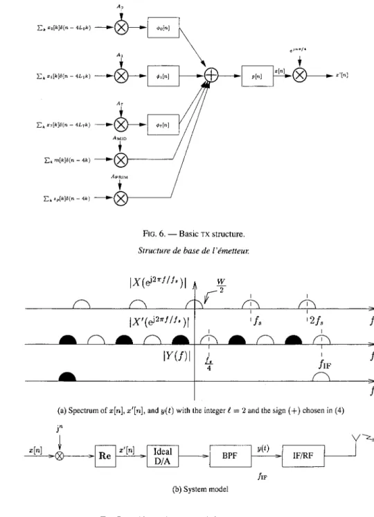
3.2. Basic Transmitter structure
The implementation of the transmitter allows for the generation a composite signal containing up to 8 variable-rate, variable power data streams per slot. It is shown in Figure 6. The rates of the different streams is
FRAME
2 r4*
. 1 2 ~694us S 17e7 I )/// z/i ~ 256 FIG. 5 . - - Slot s t r u c t u r e .Structure des crdneaux temporels
UPLINK SLOT
DOWNLINK SLOT
~ ] . . . aS DOWNLINK SLOT (with SYNC)
v
I - z - r l
338 C. BONNET - AN OPEN SOFTWARE-RADIO ARCHITECTURE SUPPORTING ADVANCED 3G+ SYSTEMS Ao
Y~k x a [ k ] 6 ( n - 4Lo k ) - - - l l ~ l ~ k
E ~ ~r[~]~(n - 4/,7/:)
FIG. 6 . - - B a s i c T X structure. Structure de base de l'dmetteur.
A A
IY(f) l
W -T I I 'f~ ' 2 f s f I I i i f "r 4flF
f
(a) Spectrum of x[n], x'[n], and y(t) with the integer g = 2 and the sign (+) chosen in (4)
jn
>|
/IF (b) System model
FIG. 7. - - Alternative approach for IF up-conversion.
Approche alternative pour la conversion en Ft.
controlled by OVSF spreading sequences d~i[n ] and the amplitudes by A i. The choice o f ~i[n] dictates the sprea- ding factor Li, which ranges from 2 n, n = 0..4.
Two possible midambles, m[k], can be inserted having lengths o f either 256 or 512 chips. These are superposition of either 3 or 8 cyclic shifts of a training sequence with a periodic extension. This structure allows for efficient channel estimation techniques based on the
Fast Fourier Transform (EFT).
The beginning o f synchronization slots (only BS) contains a p r i m a r y synchronization sequence Sp[k] of length 256 chips superimposed on the data.
The composite signal is filtered by a 12-tap root-raised cosine FIR filter, p[k], which simultaneously
up-converts the signal to a carrier frequency of n/2. To this end, we choose the sampling rate foac according to the classical expression
f,F
(4) foac-- f + 1/---4- for a positive integer Then, we generate the discrete-time real signal (5) x'[nl=Re{x[n]eJ2X~/f~A,)n} =Re{j+-nx[n]}
In this way, the periodic spectrum of x'[n] shows a spectrum replica centered at f/F (see Fig. 7(a)). After D/A conversion, a pass-band filter centered at fl F removes the other replicas, generating the desired IF modulated signal.
C. BONNET -- AN OPEN SOFTWARE-RADIO ARCHITECTURE SUPPORTING ADVANCED 3G+ SYSTEMS 339
--.:.~--~--AIX'(4>~:/:")[.,,?..-~"----~
t ~-. N- - " s l s i n c ( f / f ' )
\
f - ~ - - . , ~ . t @ - ~ .f' .IF
(a) D/A frequency response without up-sampling
, f
/IF fe
(b) D/A frequency response with up-sampling
FIG. 8. - - D/A f r e q u e n c y r e s p o n s e .
Rdponse en friquence de la CNA.
The discrete-time modulation by
fDAC/4
in (5)requires a negligible computational cost since it corres- ponds to change alternatively the signs of
x[n]
as can be noticed in expanding equation (5). In order to avoid alia- sing when taking the real and imaginary part, the sam- piing rate must satisfy also theconditionfDac > 2W.
I:~( ~2":/:')I kF
f1F rate f,
2,
)
the location of the start of a frame. This is achieved by filtering the bandpass received signal
r[n]
asf 2 5 5 ] 255
(6)
rs[n]=[k~=oSp[k]5(n+4k)l* r[n]=~=oSp[k]r(n+ak )
and averaging the r,[nl 2 over several frames. The maxi- m u m output of this filter is used to adjust the receive signal strength (via a variable gain IF amplifier) and syn- chronization is achieved when the maximum is greater than a pre-defined threshold. Note that this filtering ope- ration involves purely real quantities. This is typically the most computationally intensive part o f the receiver front-end since it requires a fairly long filter operating at the sampling rate. The 3GPP standard uses a hierarchicalFIG. 9. - - Receiver front-end.
T~te de rdcepteur.
111.3. R e c e i v e r
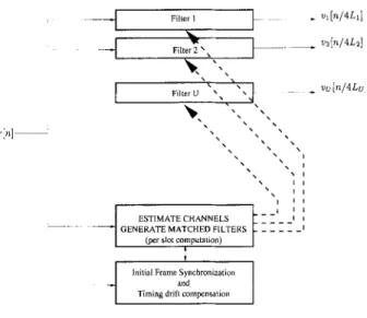
In this section we analyze some of the theoretical aspects o f the receiver signal-processing. In particular we give a description of the receiver front-end architecture shown in Figure 10. Then we focus on channel estima- tion, matched filter synthesis and symbol detection.
111.3.1. F r a m e Synchronization
Frame synchronization is achieved using a filter mat- ched to the primary synchronization sequence to estimate
r [ < n - - ~ [ Filter 1 . v l [ n / 4 L l ] .... ~ l Filter 2 "~ ~,
~.,"
[ FilterU " - . " ~ - v v [ n / 4 L u i'~.
ESTIMATE CHANNELS . . . GENERATE MATCHED FILTERS(per slot computation
-. Initial Frame andSynchr~176 Timing drift compensalion
x x
f!
-:___FIG. 10. - - Basic RX structure.
Structure de base du rdcepteur.
340
lid s p , 1 [k]
C . B O N N E T - - A N O P E N S O F T W A R E - R A D I O A R C H I T E C T U R E S U P P O R T I N G A D V A N C E D 3 G + S Y S T E M S
1 m Of
FiG. 11. - - Primary Synchronization Processing.
Traitement de la synchronisation primaire.
structure for the primary synchronization sequence which allows the filter to be implemented as a concatena- tion of 2 FIR filters of length 16. A block diagram of the primary synchronization sequence is shown in Figure 11.
I I I . 3 . 2 . C h a n n e l e s t i m a t i o n
Here we consider the training-sequence based multi- user channel estimation procedure for block-synchronous COMA described in the UMTS/TDD standard.
In this scheme users are roughly synchronized to a common time-reference and transmit the training sequence at the same time (user timing errors are inclu- ded as an effect of the channel and taken automatically into account by the estimation procedure). The maximum channel length (including possible timing errors) is Q symbols and the training sequence sent by each u-th user is a cyclic shift of the same common base training sequence m = [m[0], re[l] ... m [ M - 111 r of length M symbols. This solution allows joint estimation of all user channels if M > QU, where U is the number of interfe- ring users. It is proposed and described in [16, 17] and with some modifications in [ 18]. The interested reader is referred to these papers and references therein for more details.
Under these assumptions we can write the received signal sampled at frequency fADC = N J c during the M symbols spanned by the training sequence as
w = M g + ~
(7) where
(8)
w : [w[0], w[1] .... w [ M N c - 1]] ris the received signal,
(9) g - _
[gi
r ... gu ... gv] r r ris a vector containing the channel impulse responses of the U users,
(10) gu =[gu[Ol,gu[l] .... g u [ Q N c - l l ] r
is the u-th user channel filter vector and v is a vector of interference plus noise__samples, assumed to be white. The M N c X M N C matrix A is defined as
(11) M = M | '
where (| denotes the Kronecker product and M is a cir- culant matrix containing all the possible cyclic sh__ifts (by columns) of the base sequence m. The matrix M is also circulant and it is unitary similar [19] to the diagonal matrix diag(-~-), where
v J
N c times
and where c~ is the Discrete Fourier Transform (OFT) of CZ. After some algebra [18], it is possible to show that the Least Squares estimation of the overall channel impulse response g is given by
(12) ~ = IDFT { D b ~ w}- }
where DFT and IDFT denote direct and inverse Discrete Fourier Transforms. The ratio of two vectors should be interpreted as the element-by-element division.
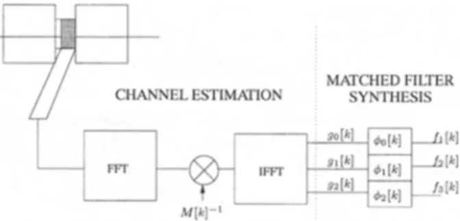
This approach can be applied to both base-band and pass-band signals. The receiver can also use the a priori information that the signal bandwidth is limited to W. Notice that this operation in the frequency domain corresponds to low-pass filtering in the time domain, moreover it reduces the computational cost since only a part of the MN C products (by the element-wise inverses o f ~ in (12)) are computed. Eventually, after the 1OFt, the processing gives the estimated channel complex enve- lope. The channel estimation procedure is summarized in Figure 12.
FIG. 12. - - Channel Estimation and Matched Filter Synthesis.
Estimation du canal et synthkse du filtre adaptd.
C. BONNET - AN OPEN SOFTWARE-RADIO ARCHITECTURE SUPPORTING ADVANCED 3G+ SYSTEMS
III.3.3. Matched Filter synthesis and data detection
Given the channel estimates, we are then interested in synthesizing a Matched Filter (MF) matched to the cas- cade formed by the user data spreading sequence, the chip pulse shape filter and the user channel. This is also shown in figure 12. The overall impulse response for code i is given by
L. 1
(13) f/(t)= 2
Oi[klg(t-k/fc)
k=O341 re-sampling techniques at both the transmitter and recei- ver front-end. These techniques have been studied in [15] and will be implemented in the next version of the software.
IV. VALIDATION OF THE EXISTING PLAFFORM
where L i is again the spreading gain. Using the sampled channel estimate
g[k]
we synthesize the discretetime fil- terfi[k] =fi(t) lt=k/fAvc
matched to the overall response as follows(14) j~[k] =
~i[k] *
g[k]In order to extract the data symbols we filter the received signal with the MF obtaining
( 1 5 ) vi[k ] = r [ k ] * j ~ * [ - k]
In this setting
r[k] is
real while f/[k] is complex so the product requires two real multiplications. On the contrary the baseband samples ofr[k]
would be at half the sampling rate but would be complex. So the two complexities are identical.Notice that the signal after matched filtering is still pass-band and the symbol estimates after subsampling are given by
(16)
[~i[k] = vi[N N k]
where
vi[k ] is
the complex envelope of the ME output. But since(17)
vi[k] = (-j)kvi[k ]
substituting into (16) and for N C = 4 we get (18)[)i[k] = ( _j)u N, kvi[N N.k] = vi[4Nk ]
In this way the symbol estimates are given by sub-sampling the ME output at symbol rate without taking care of the demodulation.
III.3.4. C a r r i e r synchronization and decoding
The carrier s y n c h r o n i z a t i o n is done at s y m b o l rate with a classical decision directed algorithm [20]. The algorithm then takes a decision on the s y m b o l s and recovers the data (in our e x a m p l e a video stream).
The platform described in this paper has been valida- ted by the transmission and the reception of two user full-duplex real-time video flows in an indoor environ- ment. Two H263 video streams are transmitted in parallel and decoded in real time. For this we use the following parameters:
9 spreading factor 16
9 bit rate 397 kbps (peak) per user
9 TDD configuration: 1 Tx slot followed by 1 Rx slot (transmission is done every 2 slots)
9 two synchronous full-duplex streams per slot 9 RF band: 5 MHz at 2.1 GHz
V. CONCLUSION
This first demonstration shows that the architecture of the platform is capable of sustaining real-time communi- cations and is thus promising for future developments. The platform is currently being enhanced and opened to both industrial and academic collaboration. The enhan- cements will consist of
9 support for multiple antenna transceivers 9 more sophisticated signal processing algorithms 9 multi user detection
9 layer 2
(RLC,MAC)
functionalityCollaboration has already begun under the label of the RNRT
(R(seau National de la Recherche en Tdld-
communications)
financing program organized by the French Ministry of Industry and Finance. Three pro- jects have been initiated covering the following topics:9 radio subsystem improvement (flexibility and sensi- tivity)
9 compliance with the 3GPP UMTS/TDD specification 9 higher-level protocol stacks
9 integration to an Ipv6 experimental backbone
I I I . 3 . 5 Re-sampling
The baseband processing algorithms such as syn- chronization, channel estimation and data detection assume that the signal is sampled with an integer num- ber,
N ,
of samples per chip. In the current implementa- tion we setN c
= 4. This solution avoids utilization ofVI. CREDITS
We would like to thank D. Margairaz and R Favrat, formerly with STMicroelectronics, Geneva, for their col- laboration in the development of the RF subsystem. In
342 c. BONNET - AN OPEN SOFD,VARE-RADIO ARCHITECTURE SUPPORTING ADVANCED 3G+ SYSTEMS
addition, the help of G. Vaucher and P. Bruchlmeier from ACORT/EPFL in the fabrication of many of the hardware components was greatly appreciated.
Manuscrit refu le 16 fdvrier 2001 acceptd le 26 avri12001
BIOGRAPHIES
REFERENCES
[1] SRIKANTESWARA (S.), REED (J.H.), ATHANAS (P.) and BOYLE (R.), "A soft radio architecture for reconfigurable platforms", tEEE
Communications Magazine, February 2000.
[2] "Special issue on software radio", tEEe JSAC, Vol. 4, April 1999. [3] "Software radio", IEEE Personnal Communications, Vol. 4,
August 1999.
[4] TSURUMI (n.) and SUZUKI (Y.), "Broadband RE stage archi-
tecture for software-defined radio in handheld terminal applications", lEEE Communications Magazine, February 2000.
[5] ZANGI (K.) and KOILPILLAIR (R.), Software radio issues in cellular base stations", tEEE JSAC, Vol. 17, pp. 561-573, April 1999.
[6] RAPPAPORT (Z.), Wireless Communications, Englewood Cliffs,
1996
[7] 3GPP-TSG-RAN-WG1, "TS-25.2XX series", tech. rep., January 2000. [8] DAHLMAN (E.), GUDMUNDSON (B.), NILSSON (M.), SKOLD (J.) and
AB (E.R.S.), "UMTS/IMT-2000 based wideband CDMA", leeE Com-
munications Magazine, Vol. 36, pp. 70-80, Septembrer 1998. [9] "http://www.itu.int/imt/2-rad-devt/index.html".
[10] FURUSKAR (A.), MAZUR (S.), MOLLER (E), OLOFSSON (H.), and
SYSTEMS (E.R.), "EDGE: Enhanced data rates for GSM and TDMM136 evolution" IEEE Personnal Communications, Vol. 6, pp. 56-66, June 1999.
[11] MOGENSEN (P.), KREDERIKSEN (E), DAM (H.), OLESEN (K.) and LARSEN (S.), "A Hardware Testbed for Evaluation of Adaptive Antennas in GSM/UMTS", Vol. tEEe PIMRS'96, pp. 540-544, Oct. 1996.
[12] XILINX, "Xilinx 2001 FPGA Databook', http://www.xilinx.com, 2001.
[ 13] PLXTECHNOLOGIES, "PC19080", http://www.plxtecj.com, 1999. [14] 3GPP, "3 ,d Generation Partnership Project", http://www.3gpp.org,
2001
[15] MONTALBANO (G.) and NORDIO (A.), "Front-end software- radio review", tech. rep., Institut Eur4com, July 1999, to be appeared.
[16] STEINER (B.) and JUNG (E), "Optimum and suboptimum channel estimation for the uplink of cdma mobile radio systems with joint detection", European Transaction on Communications, Vol. 5, pp. 39-49, Jan.-Feb. 1994.
[17] 3GPP-TSG-RAN-WG1, "XS-25.221v3.1.0; physical channels and mapping of transport channels onto physical channels (TDD)",
tech. rep., January 2000.
[18] CAIRE (G.) and MITRA (U.), "Structure multiuser channel estima- tion for block-synchronous DS/CDMA", Submitted to IEEE Tran-
saction on Communications, July 1999.
[19] GOLUB (G.H.) and LoAN (C.EV.), Matrix Computation, The John
Hopkins University Press, 1996.
[20] PROAKIS (J.G.), Digital Communications, MY." McGraw Hill, 2 "ded., 1989
[21] "Spectrum Signal Processing", http://www.spectrumsignal.com, 2001.
[22] FSMLABs, "RTLinux', http://www.rtlinux.org, 2001.
Christian BONNET joined Institut Eurecom as an associate professor in 1992. Since 1998 he is at the head of the Mobile Communications Department of Eurecom. His teaching activities are distributed and reaitime systems, mobile communication systems, wireless LANS and protocols for mobility management. His main areas of research are wireless protocols, wireless access to IP Networks and data communi- cations in mobile networks including mobile ad hoc networks. He is currently participating in research projects related to UMTS in the field of QOS and Ipv6: (IST) Mobydick, (RNRT) SAMU, PLATON, @IRS++. He has been the team leader of Eurecom for the European project (ACTS)
WAND (Wireless ATM Network Demonstrator) and responsible for pro- jects in wireless network simulations (GSM) and wireless LAN inter- connection with ATM. Before joining Eurecom he was a consultant in the GSI group for 9 years where he worked on different projects rela- ted to radio telecommunications, value added networks and real time networks. He participated to the European projects (ESPRIT) DES-
CARTES, DRAGON, REX. He was appointereceiver Director of the Real Time Department of GSI Tecsi. Christian Bonnet was born in Paris on September 17, 1955. He received an engineering degree from t~cole Nationale des Mines de Nancy in 1978. He first worked for Alsys where he participated in a compiler production project for ADA. Ginseppe CAIRE was born in Torino, Italy, on May 21, 1965. He received the BSc in Electrical Engineering from Politecnico di Torino (Italy), in 1990, the MSc in Electrical Engineering from Princeton Uni- versity (USA) in 1992 and the PhD from Politecnico di Torino in 1994. He was a recipient of the AEI G.Someda Scholarship in 1991, has been with the European Space Agency (ESTEC, Noordwijk, The Netherlands) in 1995, was a recipient of the COTRAO Scholarship in 1996 and a CNR Scholarship in 1997. He has been visiting the Institute Eurecom, Sophia Antipolis, France, in 1996 and Princeton University in summer 1997. He has been Assistant Professor in Telecommunications at the Politecnico di Torino and presently he is Associate Professor with the Department of Mobile Communications of Eurecom Institute and Associate Editor of the 1EEE Transactions on Information Theory. He is co-author of more than 30 papers in international journals and more than 50 in intemational conferences, and he is author of three international patents with the European Space Agency. His interests are focused on digital communications theory, information theory, coding theory and multiuser detection, with particular focus on wire- less terrestrial and satellite applications.
Alaln ENOUT received his engineering diploma in signal processing from ISMRa (Institut des Sciences de la Matirre et du Rayonnement, t~cole Nationale Superieure d'Ingenieur de Caen) in 1986. He also recei- ved a Diplrme d'l~tudes Approfondies in instrumentation and control. He worked four years at the Center for Energy of the l~cole des Mines de Paris where he was involved in optimal control and numerical simulation. Then he joined ISTAR (Imagerie Strr4o Appliqu4e au RelieD, a company working in Digital Terrain Model automatic extraction from digital images, as system manager for four years. He joined Eurecom in 1997 where he worked on the WAND (Wireless ATM Network Demonstrator) European project. He is currently involved in the UMTS project in the Mobile Communication Department.
Pierre A. HUMBLET received the Electrical Engincer degree from the University of Louvain, Belgium, in 1973, and the MSEE and Phi) degrees from the Massachusetts Institute of Technology, Cambridge, MA. After graduating in 1978 he remained at M1T where he became a
C. BONNET - AN OPEN SOFTWARE-RADIO ARCHITECTURE SUPPORTING ADVANCED 3G+ SYSTEMS
Professor of Electrical Engineering. In 1993 he became head of the Mobile Communications department of the Eurecom Institute in Sophia Antipolis, France. In 1998 he joined Astral Point Communications where he is Chief Technical Officer, while still serving as an adjunct professor at the Eurecom Institute. His teaching and research interests are in the area of communication systems, particularly mobile digital networks and optical networks. He was elected a Fellow of the IEEE.
Giuseppe M O N T A L B A N O received the MSc degree in Electrical Engineering and the PhD degree (Hons.) in Electrical and Communi- cations Engineering both from Politecnico di Torino, Turin, Italy, in 1995 and in 1999, respectively. From March 1994 to February 1995 he was with "Istituto Galileo Ferraris di Torino", Torino, Italy, working in the area of non-linear optical devices. In 1995, he was with CSELT, Torino, Italy, working on the design and DSP implementation of adap- tive signal processing algorithms for antenna array processing on GSM base stations. From November 1995 to November 1998, he was with the Dipartimento di Elettronica of Politecnico di Torino as a PhD stu- dent supported by CSELT. From September 1997 until October 1998, he was scientific visitor at InstituI Eur6com. In November 199S, he joi- ned the Mobile Communications Department of InstituI Eur6com as a research and teaching associate working on the design of a software radio platform for UMTS-TDD. He joined Philips Semiconductors in December 2000 where he is currently working as a DSP system engi- neer on UMTS. His rescarch interests include DSP systems design, signal processing and digital communications theory, with particular regard to spatio-temporal techniques for wireless communications.
Alessandro N O R D I O received the Engineer degree in Telecommuni- cations Engineering from Politecnico di Torino, Italy, in July 1998. From August 1998 to December 1998 he has been with Dipartimento di Elettronica of Politecnico di Torino where he worked as a consul- tant for Omnitel. In January 1999 he joined the Mobile Communica- tions Department of Institut Eurdcom as a PhD student. His research interests are in the field of signal processing, synchronization and multi-user detection.
Dominique NUSSI-IAUM was born in Thann, France, on August 14, 1971. He received an engeneering degree from l~cole Sup6rieure d'l~lectricit6 in 1994 and a PhD from Universit6 de Rennes, France in 1999. From October 1995 to March 1999, he was with TDF (T616diffu- sion de France), working on the design and realization of a FM digital receiver. In May 1999, he joined the Mobile Communication Depart- ment of Institut Eurecom as a research engineer. He is curretly the Software Radio Platform Developement Manager, in the Mobile Com- munication Department.
T h o m a s H O H N E received his MSc degree from the Technical Uni- versity of Berlin in 1996 in telecommunications. His main activities at the xu Berlin were directed towards spread spectrum systems and spreading sequences. In 1996 he joined the Swiss Federal Institute of
343
Technology in Lausanne, first as a postgrad student in the communica- tion systems devision, then as assistant in the Mobile Communications Lab. Since 2000 he is with the Radio Communications Lab of the Nokia Rescarch Center, Helsinki, working at an UMTS-trial system.
R a y m o n d K N O P P was born in Montreal, Canada, on January 20, 1969. He received the B.Eng. (Honours) and the M.Eng. degrees in electrical engineering from McGill University (http://www.ee.mcgill.ca), Montreal, Canada, in 1992 and 1993, respectively. In 1997, received the PhD degree in communication systems from the Swiss Federal Institute of Technology (EPFL,http://www.epfl.ch), Lausanne. During his PhD studies (1993-1997), he was a Research and Teaching Assistant in the Mobile Communications Department of Institut Eur6- com (http://www.eurecom.fr), Sophia Antipolis, France. From 1997-2000 he was a research associate in the Mobile Communications Laboratory (LCM-EPFL) of the Communication Systems Department (http://dscwww.epfl.ch) of the Swiss Federal Institute of Technology (EPFL), Lausanne. In 2000 he rejoined the Mobile Communications Department of Institut Eur6com as an Assistant Professor. His current rescarch interests are in the area of digital communications, coding, multiple-access, power-control techniques in radio communications, software radio architectures, and implementation aspects of digital communication systems.
Bixio R I M O L D I was born in Bellinzona, Switzerland, on August 31, 1956. He received both his Dipl. El.Ing. degree and his Doctorate es Science degree from the Swiss Federal Institute of Technology in Zurich (ETHZ). During 1988-1989 he had visiting positions at the Uni- versity of Notre Dame and Stanford University, respectively; In 1989 he joined the faculty of Electrical Engineering at Washington Univer- sity, St. Louis, where in 1994 he was promoted to Associate Profes- sor. Since 1997 he is a professor at the Swiss Federal Institute of Technology in Lausanne (EPFL) and director of the Mobile Communi- cations Lab. His research and teaching interests are in digital commu- nication systems, information theory, and coding. Dr. Rimoldi is an IEEE fellow and an associate editor of the European Transactions on Telecommunications. In 1993 he received a US National Science Foundation Young Investigator Award (NYI). He has been co-chair (with Bruce Hajek) of the 1995 IEEE Information Theory Workshop on Information Theory, Multiple Access and Queueing, and will co-chair (with James L. Massey) the 2002 International Symposium on Information Theory.