HAL Id: hal-02357172
https://hal.archives-ouvertes.fr/hal-02357172
Submitted on 10 Nov 2019
HAL is a multi-disciplinary open access
archive for the deposit and dissemination of
sci-entific research documents, whether they are
pub-lished or not. The documents may come from
teaching and research institutions in France or
abroad, or from public or private research centers.
L’archive ouverte pluridisciplinaire HAL, est
destinée au dépôt et à la diffusion de documents
scientifiques de niveau recherche, publiés ou non,
émanant des établissements d’enseignement et de
recherche français ou étrangers, des laboratoires
publics ou privés.
Distributed under a Creative Commons Attribution| 4.0 International License
To cite this version:
Hélène Hourdequin, Lionel Laudebat, Marie-Laure Locatelli, Zarel Valdez Nava, Pierre Bidan.
Metal-lized ceramic substrate with mesa structure for voltage ramp-up of power modules. European Physical
Journal: Applied Physics, EDP Sciences, 2019, 87 (2), pp.20903. �10.1051/epjap/2019180288�.
�hal-02357172�
Eur. Phys. J. Appl. Phys. 87, 20903 (2019) c
H. Hourdequin et al.,EDP Sciences, 2019
https://doi.org/10.1051/epjap/2019180288
Regular Article
Metallized ceramic substrate with mesa structure for voltage
ramp-up of power modules
?
H´el`ene Hourdequin1, Lionel Laudebat1,2,*,Marie-Laure Locatelli1, Zarel Valdez-Nava1,
and Pierre Bidan2
1LAPLACE, Universit´e de Toulouse, CNRS, UPS, INPT, Toulouse, France 2
Universit´e de Toulouse, Institut National Universitaire Champollion, Toulouse, France
Received: 30 September 2018 / Received in final form: 19 April 2019 / Accepted: 15 July 2019
Abstract. As the available wide bandgap semiconductors continuingly increase their operating voltages, the
electrical insulation used in their packaging is increasingly constrained. More precisely the ceramic substrate, used in demanding applications, represents a key multi-functional element is being in charge of the mechanical support of the metallic track that interconnects the semiconductor chips with the rest of the power system, as well as of electrical insulation and of thermal conduction. In this complex assembly, the electric field enhance-ment at the triple junction between the ceramic, the metallic track borders and the insulating environenhance-ment is usually a critical point. When the electrical field at the triple point exceeds the critical value allowed by the insulation system, this hampers the device performance and limits the voltage rating for future systems. The solution proposed here is based on the shape modification of the ceramic substrate by creating a mesa structure (plateau) that holds the metallic tracks in the assembly. A numerical simulation approach is used to optimize the structure. After the elaboration of the structures by ultrasonic machining we observed a significant increase (30%) in the partial discharge detection voltages, at 10 pC sensitivity, in a substrate with a mesa structure when comparing to a conventional metallized ceramic substrate.
1 Introduction
Power electronics is at the dawn of an important evolution thanks to the significative introduction of wide bandgap (WBG) semiconductors into power electronic systems.
Indeed, the evolution of the technology based on sili-con carbide (SiC) allows the development of chips able withstanding voltages greater than today ratings (for silicon devices), along with potentially higher switch-ing frequencies [1]. The availability of very high voltage demonstrators (such as bipolar diodes [2] and transistors [3–5]), opens the way to a major evolution in the field of power electronics but at the same time stresses the need to develop new packaging strategies in this race towards the feasible-highest-voltage SiC device and power mod-ule. In current packaging strategies, increasing the voltage requires, almost directly, a higher dielectric strength of the insulating materials. Naturally, if the constraints imposed continue to increase, the intrinsic physical limits will be attained.
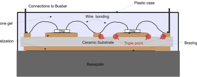
The typical structure of a 6.5 kV silicon Insulated Gate Bipolar Transistor (IGBT module) is shown in Figure 1. The three main functions of a module’s packaging are to protect and isolate the chip from its environment, to evacuate the heat dissipated by the chips, and finally to provide an electrical connection between the chips and the ?
Contribution to the Topical issue “Electrical Engineering Symposium (SGE 2018)”, edited by Adel Razek.
*e-mail:[email protected]
power terminals. Inside the module, the semiconductor chips are brazed to a metallized ceramic substrate, which must be both an excellent thermal conductor and electri-cal insulator. The most commonly used ceramic materials are alumina (Al2O3), silicon nitride (Si3N4) and aluminum
nitride (AlN). The metallization is generally carried out by a thick layer of copper, which is connected by an oxide, either by an eutectic bonding process (“Direct Bonded Copper”, DBC), or by an active metal brazing process (AMB). The ceramic substrate is then fixed on a base-plate (e.g., AlSiC), which ensures the mechanical integrity of the assembly and the heat transfer to the cold source. The entire assembly module is generally immersed in an encapsulating material, typically a silicone gel, to provide dielectric protection along the surfaces of the substrate and between other parts of the module subject to strong electric fields. An epoxy resin can be used to mechani-cally reinforce the structure, in particular the connections [6]. The connections on the front of the chips are pro-vided by bonding wires, ribbons [7] or pins [6], in order to electrically connect the various chips and tracks.
The aim of this article is to propose an original solu-tion for integrating future very high voltage components. We considered as a base for our study, a device of 15 kV, to match the components that are currently in the devel-opment phase [8,9]. The study focuses on a particularly critical area, called the triple point area, situated at the intersection of the insulating substrate, metallic track and encapsulation, as specified in Figure 1. This area is the location of an electric field reinforcement that will
Fig. 1. Schematic cross-section of plastic power module. Some triple points localisations are illustrated.
particularly stress the insulation of the system in case of voltage rating increase. In order to ensure the reliability of the future higher voltage systems, it is essential to focus research on ways to reduce the impact of high electri-cal stresses inside packaging, without (too) penalizing the performance in terms of heat dissipation, high frequency operation etc. The paper will first review different solu-tions, which are in use or have been proposed in the literature. Then, the principle and the theoretical poten-tiality of the metallized substrate mesa structure proposed here will be presented, followed by the description of the experimental study and the discussion of results.
2 Classic strategies to reduce electric field
constraints
The evolution of the voltage levels usually leads to an increase in the thickness of the insulation, or/and to the choice of a material with a higher dielectric strength. Moreover, in case of simultaneous high-power level (i.e. high currents), a higher thermal conductivity may also be a criterion of choice. In practice today, in the power mod-ules, the thickness of the substrate is 0.320 mm for low voltage modules, 0.635 mm for modules between 1.7 kV and 3.3 kV and 1 mm for 6.5 kV modules. The latter is the maximum thickness used in conventional modules because beyond this thickness, the degradation on the thermal resistance is too great, though using aluminium nitride (AlN), which is the available ceramic material affording both the best electrical and thermal properties (comparing to Al2O3and Si3N4).
It is in this context that in the recent past years, differ-ent ways have been proposed to better sustain or to reduce the electric field values, without increasing the thickness of the insulating substrate, namely consisting into [10]:
– Improve the dielectric properties (breakdown electric field or partial discharges resistance) of the volume encapsulation insulation, often by the modification of the polymeric encapsulation (addition of micro and/or nanoparticles) [11].
– Add a thin coating in the insulation system, like a polyimide (PI) or polyamide-imide (PAI) film [12], to improve the voltage withstand at the specific point of the greatest stress, either to spread the equipo-tentials with linear semi-resistive varnishes based on hydrogenated amorphous silicon (a − Si : H) [13], or non-linear semi-resistive varnishes based on poly-imide filled with micro-particles of zinc oxide (ZnO) [14].
– Locally improve the dielectric properties of the encapsulation insulator using anisotropic materials or properties gradient materials Functionally Graded Materials (FGM) [15]. It is an electric field grading approach using composite materials and an in-situ elaboration process allowing a self-adaptive permit-tivity gradient, located where the constraints are strongest [16–18].
– Design the tracks geometry by optimizing the met-allization edges [19], by burying the tracks in the substrate [20] or by raising the metallization with a rounded geometry [21].
The common factor in all of these solutions is that they address the electric field relief by modifying the polymeric encapsulation material or the interface between the sub-strate and the encapsulation. In this study, we present an original structure to reduce the intensity of the electric field, both in the ceramic part and in the encapsulat-ing, based on a geometric modification of the ceramic substrate.
3 Method and proposed solution
The modelling approach is based on an evaluation and optimization of the geometry of the packaging using a numerical simulation tool with the finite elements as a means of preliminary dimensioning. The finite element method (FEM) used allows simulating the electric field distribution inside the power module, in order to evaluate the effect of varying material properties and architecture features. In particular, the simulation provides quanti-tative results on the electric field for different substrate
H. Hourdequin et al.,: Eur. Phys. J. Appl. Phys. 87, 20903 (2019) 3
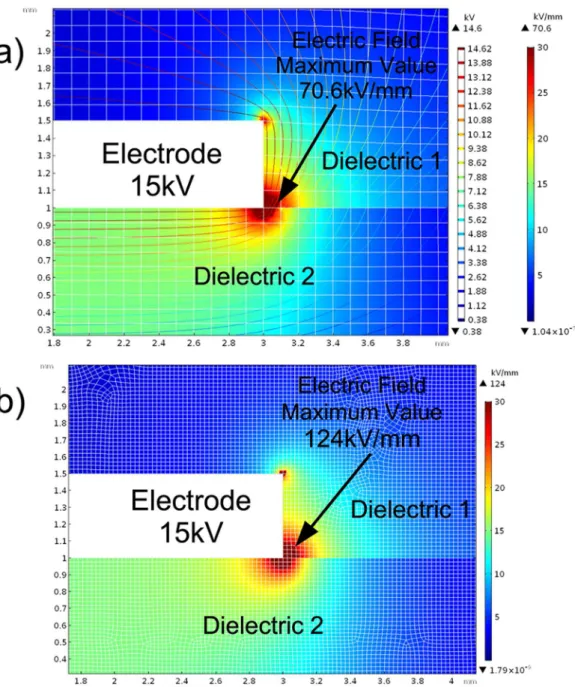
Fig. 2. Comparison of the maximum value of the electric field for 2 different mesh sizes (100 µm on the left and 25 µm on the
right) of the same geometry. The meshes are draws in white.
configurations comparison. An electrostatic analysis has been performed by solving the following equations:
4V = −ρ ε0 (1) − → E = −−→∇V. (2)
Unlike the magnetic field, the electric field is diver-gent (according to the Maxwell-Gauss equation div−→E = ρ/ε0 where ε0 is vacuum dielectric constant (8.85 ×
10−12F m−1).
From a numerical point of view, the theoretical value of the field tends to infinity. Such a singularity exists at the triple point and a numerical solution will be very sensitive
to mesh resolution, this well-known problem is described in [22]. Therefore, for same structure and potential supply conditions, the main parameter that influences the electric field value close to the zones of divergence is the mesh. To illustrate this, the electric field is simulated with the same geometry for two different meshes in Figure 2.
In order to study the electrical insulation system of the power module, the ceramic substrate, the encapsulating silicone gel and the copper electrodes are considered for the simulation. The material parameters are respectively a permittivity equal to 2.7 for dielectric 1 (silicone gel) and 9 for dielectric 2 (ceramic). The 2D problem is solved by applying an electrostatic model by means of a commercial FEM tool, i.e. Comsol Multiphysics 5.3a. The maximum magnitude of the electric field is estimated for
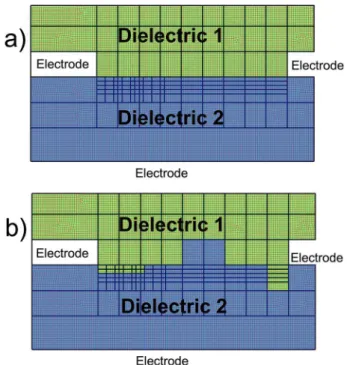
Fig. 3. Example of 2 different topologies, based on a predetermined geometry (black lines) and the mesh frozen (0.025 mm2× 0.025 mm2 mesh square in red).
each material. Different representations of polygon meshes may be used for different applications and goals. Here, the structure is described using a quadrilateral mesh, drawn in white as shown in Figure 2. The simulation is presented for two mesh sizes ((a) on the top mesh with 100 µm and on the bottom (b) mesh with 25 µm). We can observe a difference between the simulation results only near the triple point and this difference is directly linked to the mesh refinement. To compare two different geometries, this dependence to the mesh represents an issue because the final characteristics of the mesh, includ-ing the minimum mesh size at interfaces, triple points, etc., depend upon the topology of the structure and are partially determined by the designer’s choices and by the meshing routine of the simulation tool (self-adaptive mesh including the boundaries between the subdomains). A way to get around the problem and allow a com-parative study of the different structures is to define a mesh a priori, adapted to consider all the topologies to be compared in the study. This approach is proposed because, in this process, we don’t want to evaluate the exact maximum field in the triple point but to compare different solutions. The significant changes in geometry did not allow to use some other methods proposed in the literature [22,23].
Figure 3 presents an example of the predetermined mesh used in this study. A generic geometry is prede-fined, in such a way that the different topologies (with different lengths and widths) to study can be described by changing only the material properties in the differ-ent squares and rectangles predefined in black. In the top Figure 3a, a classical metallized ceramic substrate is presented, where the elements in green (respectively in blue) are made of dielectric 1 (respectively dielectric
Fig. 4. Geometry for “Conventional structure” simulation.
Fig. 5. Change in geometry of a conventional metallic substrate
to mesa structure.
2). Another topology represented in Figure 3b has been obtained assigning dielectric 1 (in green) and dielectric 2 (in blue) to other predefined areas, as wanted. This method has allowed to compare the different solutions under simulation without suffering from numerical arte-fact due to induced mesh variations. Indeed, the mesh is generated in the beginning with the predefined structure and frozen for the different changes in the topology for the study. A quadrilateral mesh is the most appropriate for the “academic” conventional and mesa structures here envisaged.
This is a basic approach to define the general trends. In a more complex approach, we could have used another type of mesh, allowing to study for additional geometries, for example to take into account copper etching [10].
3.1 Definition of the conventional structure
The basic simulated structure corresponds to a metallized AlN substrate 1 mm thick with vertical copper edge pro-file. Encapsulation is conventionally made of silicone gel. Two top electrodes are separated by 2 mm and a third elec-trode is placed on the rear side of the substrate (Fig. 4). These electrodes are considered as perfect conductors. On the left electrode, an electrical voltage of 15 kV is sup-plied (terminal) and the other electrodes are connected to the ground. Silicone gel conventionally provides the encapsulation.
Thereafter this structure is considered as a “reference”, the simulation results after the structure modifications are compared with it.
3.2 Definition of the Mesa structure
The aim is to create a structure, which can improve the distribution of the electric field at the triple point. Figure 5 presents the principle of the mesa structure which consists in creating a trench at the bottom of the two electrodes of the conventional structure. Indeed, the metallization of copper is flush with the vertical side, bur-rowed in the ceramic, forming a plateau (mesa). As we will see below, the distribution of the electric field at the triple
H. Hourdequin et al.,: Eur. Phys. J. Appl. Phys. 87, 20903 (2019) 5
Fig. 6. FEM simulation of the conventional structure (Fig.4).
point will depend on the permittivity and the conductiv-ity of the materials (permittivconductiv-ity, conductivconductiv-ity) and the geometrical parameters of the mesa, which are the height h and the width e of the groove (as defined in Fig.5).
In order to estimate the benefits on the reduction of the maximum electric field, a finite element study (FEM) of the proposed structure is carried out with Comsol Multiphysics software.
4 Modeling: study of the electric field
distribution by simulation
4.1 Preliminary simulation of mesa structure
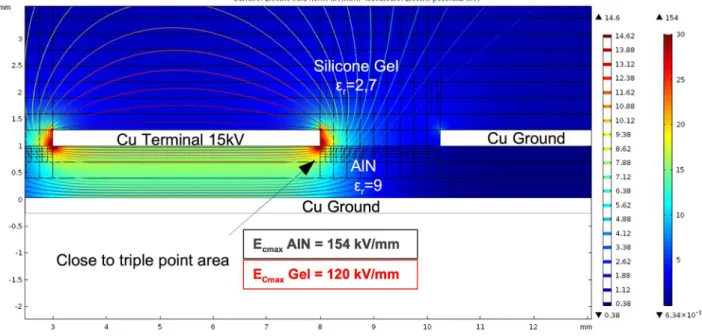
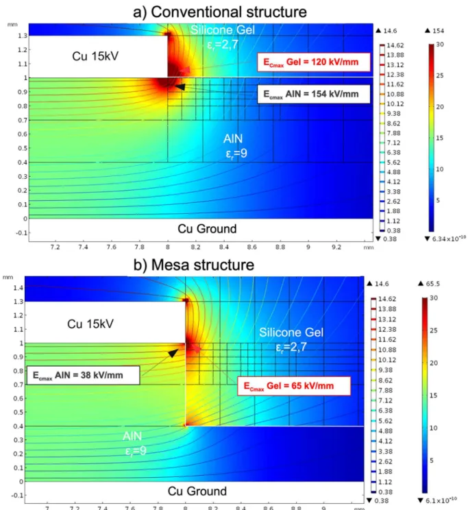
The FEM simulation of the reference structure (Fig. 4) with equipotential lines and electric field magnitude is presented in Figure6. The black straight lines in the sil-icone gel or AlN are not corresponding to the mesh, but to the predefined geometry as explained above. The color scales are defined in the figure. The material parameters are only the permittivity of the ceramic (AlN) and of the silicone gel, respectively equal to 9 and 2.7. We can clearly observe that the electric field stress is concentrated on the triple point area. The second electrode, beside the termi-nal doesn’t influence the electric field in the considered case. Now, we will focus on the triple point. At the top for conventional structure, the magnitude field distribution is shown (Fig.7) exhibiting a maximum value of 154 kV/mm at the triple point in this reference case.
Considering 0.6 mm thick mesa structure (Fig. 5), enables to decrease the maximum electric field down to 65 kV/mm, which means that the stress at the triple point is considerably lowered (decrease of 57% in comparison with the conventional structure). Indeed, by compar-ing the maximum values of the electric fields in both
cases, the maximum values in the silicone gel drop from 154 kV/mm to 38 kV/mm and in the ceramic decrease from 120 kV/mm to 65 kV/mm.
It is possible to discern the displacement of the max-imum stress from the ceramic in the classical structure towards the silicone gel in the mesa structure. The encap-sulating material enduring the highest electrical constraint without the mesa structure package becomes the insulat-ing material of greatest constraints under electrical field in the mesa structure. However, the areas of maximum stress (triple points) don’t match with defects areas, such as air bubbles more likely to appear at the foot of the reliefs during the implementation of the encapsulation. Thus, from the point of view of partial discharges, the mesa structure should make it possible to increase their threshold of appearance, thanks to weaker electric fields in the sensitive zones.
4.2 Mesa structure optimization strategy
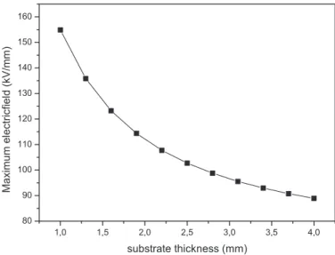
Other heights of the mesas h, ranging from 0 to 0.6 mm, were tested in order to evaluate the effect on the triple point for a 1 mm thick substrate. Figure 8 (black line) shows that the relationship between the electric field at the triple point and the height of the mesas is inversely exponential. It is shown, that a significant diminution of the electric field at the triple point, by the creation of the mesa in 1 mm thick substrate, can be obtained. While almost no deterioration of the thermal resistance is induced, in comparison with the reference structure.
Nevertheless, as the electric field values for 1 mm sub-strate remain still high compared to current material’s dielectric strengths, the case consisting in doubling the thickness of the AlN substrate has been simulated as well (Fig. 8, red line). The same significant effect of the mesa design is observed. In this latter case, a further reduction
Fig. 7. Comparison of electrostatic simulations for (a) conventional structure and (b) mesa structure.
of the field stress is obtained, compared to the reference structure.
To prove the asset of the mesa structure, a comparison with the conventional one was made. The simulations indi-cate that, even by increasing the AlN substrate thickness up to 3 mm, the resulting reduction in the electric field at the triple point (presented on Figure 9) can never be as significant as it can be for a thinner substrate (Fig.8) with a relatively small height (0.2 or 0.3 mm) of the mesa structure [24].
For several width e of the groove, in same simulation conditions, we have determined the maximum electric field
in the structure for a unique height h of mesa (Fig. 10). Beyond a groove width close to 0.5 mm, the equipotential distribution is such that the value of the maximum electric field at the triple point becomes constant as a function of e.
As you can imagine, confirmed by the simulations (not presented here, cf. [10]), the misalignment of the met-allization with the substrate and the inclination of the walls of the ceramic to the vertical have a very strong impact on the value of the electric field at the triple point. The optimum (i.e. minimum) electric field values are obtained for vertical sides and a perfect alignment
H. Hourdequin et al.,: Eur. Phys. J. Appl. Phys. 87, 20903 (2019) 7
Fig. 8. For two different thicknesses of the substrate in AlN,
simulation results of maximum electric field at the triple point as a function of the height of mesa.
Fig. 9. Maximum electric field at the triple point as a function
of substrate thickness for the conventional structure.
between the metallization and the substrate. This high-lights the importance of these geometric features for the implementation of the mesa structure.
5 Experimental procedure
5.1 Direct manufacture of a ceramic with a mesa structure
In order to propose prototypes, several implementation techniques have been analysed that can be classified into two categories:
– The manufacture of the ceramics in mesa form, then after the metallization.
– The forming process of the mesa structure from a metallized substrate and thus a removal of the ceramic and the metal during the operation.
Fig. 10. Simulated maximum electric field magnitude at the
triple point versus mesa width e (fixed sidewall height 0.3 mm).
The ceramic substrate can be prepared by the conven-tional path from the ceramic powder. The mesa shaping can be achieved during sintering in a preformed mesa mold or by raw machining of the ceramic before sintering.
New technologies for Additive Manufacturing (AM) of ceramic pieces can open the way to producing complex geometries, such as the proposed mesa structure for the ceramic substrate. Among the AM techniques, there is the StereoLithography Apparatus [25], that polymerizes a ceramic slurry containing a photosensitive binder in a layer-by-layer deposition method or by simultaneously sintering each layer of the ceramic by Selective Laser Sintering [26]. Nevertheless, it has a limitation on some types of ceramics, in particular a difficulty to implement AlN [27]. In addition, this mesa’s shaping solution requires a posteriori metallization of the ceramic. Industrially, it is achieved using metal sheets, generally copper or alu-minium, several hundred micrometers. Various processes for transferring these sheets to the ceramic substrate cur-rently exist, the most common of which are the “Direct Bonded Cooper” DBC (or DBA for Aluminum) and the “Active Metal Brazing” AMB, according to the type of ceramic [28,29]. A “laboratory” solution would have been to metallize a thin layer, for example by screen printing or PVD, but this configuration would not have been rep-resentative of a power electronics structure with tracks several hundred microns thick.
Whichever way solutions considered for the metalliza-tion, the problem of centering (Fig.11) of the electrode on the ceramic mesa is an important difficulty. To get around the problem, we proposed to form the mesa’s structure from a substrate already metallised.
5.2 Preparation of mesa structure starting from a metallized substrate
Another approach is to remove the “excess” material from an already metallized substrate to create the mesa structure. In this case, the solutions envisaged may
Fig. 11. Schematic representation of centering problems of
metallization.
be mechanical machining, laser ablation or ultrasonic machining by trying to ensure alignment of the flanks between the metal and the ceramic.
Mechanical machining by milling or coring of the ceramic can be achieved by a diamond tool by providing a thermal cooling system to overcome the rise in temper-ature taking into account the good thermal conductivity of the ceramic. But this technique comes up against the difficulty of removing two materials of different hardness in one pass to get flanks well aligned between the two materials.
Laser ablation has also been considered. Indeed, among many applications of laser, is machining. Compared to traditional etching techniques, laser has the advantage of not causing mechanical pressure on the work piece, since it is a non-contact and therefore fatigue-free tech-nique for tools. The choice of the laser will depend on the type of laser/material interaction. These interactions will depend on both, the laser source (wavelength, time application and the power density) and the material (its nature: metal, semiconductor, dielectric, its physical prop-erties: optical, thermal and surface condition) [30]. The thermal effect generated by the laser/material interaction represents a weak point that can nevertheless be partially overcome by the use of a pico or femto-second laser with a quasi “athermic” process. However, the different nature of the materials remains a difficulty for this technique because the necessary vertical alignment between metal-lization and ceramic can be compromised at the area of the impact zone. Finally, to ensure that the physico-chemical properties of the substrate have not been modified, espe-cially at the surface, an analysis of the post-machining material must be performed [31].
The last technique considered is ultrasonic machin-ing, which makes it possible to avoid the difficulties encountered by traditional machining, in order to ensur-ing alignment between the copper electrode and the ceramic substrate. This is the solution chosen for the implementation of our first test structures, as detailed below.
5.3 Sample preparation by ultrasonic machining
Ultrasonic machining is a subtractive manufacturing pro-cess that reproduces a given shape by abrasion. It is particularly suitable for machining hard or fragile and brittle materials (only a small mechanical pressure is applied on the part). This abrasion is achieved by a sonotrode at low amplitudes and high frequencies (greater than 16 kHz) chosen according to the material to be machined (Fig. 12). The vibration is transmitted to the
Fig. 12. Schematic of ultrasonic machining process. The tool
(sonotrode) motion transmits the vibration towards the sus-pended particles in water (slury) which in tunr erode the sample at the end of the tool.
Table 1. Ultrasonic machining parameters used for the
elaboration of samples.
Sonotrode frequency >10 kHz Particle type Silicon carbide Particle concentration in slury 400–600 particles/cm3 Tool material Polycrystalline diamond
(metal-bonded diamond)
Tool diameter 1 mm
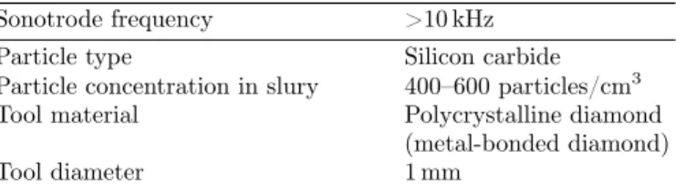
end of the sonotrode in slurry, usually consists of abrasive boron carbide, aluminum oxide or silicon carbide parti-cles in a suspension of water. This flow of slurry allows the cutting waste to flow away. The sonotrode removes material from the work piece by abrasion where it con-tacts it, so the result of machining is to cut a perfect negative of the sonotrode’s profile into the work piece. Ultrasonic vibration machining allows extremely complex and non-uniform shapes to be cut into the workpiece with extremely high precision. The ablation parameters that were used to erode copper and aluminum nitride in a single program are given in Table 1.
6 Results and discusion
6.1 Characterization of the shape of the mesa structure
Eight samples, from 1 mm thick AlN ceramic substrates, metallized with 300 µm copper (DBC), with 20 mm diam-eter round metallization patterns on the upper face were machined by ultrasound. Microcertec Corporation machines the samples.1 The vertical wall height h of the
mesa for the ultrasonic machining is 250 µm with a gorge width e of 1 mm (without integrating the fillet of the tool of about 100 µm).
A cross-sectional view of a sample is shown in Figure13. Before cutting purpose, the sample is encapsulated with epoxy resin. Note the very good alignment between the metallization, the mesa and the vertical profile of the ceramic’s flanks. Notice, however, that the machining seems to have impacted the edge of the copper as shown in the cross-sectional view of Figure13by the appearance of a “protuberance” of copper on the upper corner which
H. Hourdequin et al.,: Eur. Phys. J. Appl. Phys. 87, 20903 (2019) 9
Fig. 13. Cross-sectional view of sample.
Fig. 14. Observation of the surface of the AlN under a
scan-ning electron microscope, in a area between an unmachined and machined part.
is also visible by an observation at Scanning Electron Microscopy (SEM).
As these samples were the company’s first tests on these materials, the final depths of the gorge measure around 494 µm for the eight samples processed. This value is much higher than the total depth of 350 µm initially planned. Ultrasonic machining is not in direct contact with the work piece (gap left between the tool and the work piece for the circulation of the liquid with particles), the control of the depth’s parameter is difficult to estimate a priori, in particularly for the shallower depths. Optimization of the parameters must be achieved according to feedback.
We have also observed the surface of AlN by SEM on unmachined and machined surfaces in order to determine the differences at the micrometer scale that can be caused by such machining (Fig.14). The observation of the bot-tom of the mesa is difficult, but we can establish that the surface machined by ultrasound seems slightly rougher. These results were confirmed by mechanical profilometer measurements with a roughness that is almost doubled (quadratic roughness of 500 nm against 290 nm for the unmachined surface). Figure 14 shows the upper part of the mesa and the beginning of the gorge, we observe that the side of the mesa is very sharp on the scale considered. We can also observe in Figure13, a curvature between the wall and the bottom of the mesa. From a manufac-turing point of view, this curvature radius depends on the
Fig. 15. PDIV measurement system.
attrition of the tool. It degrades over time and must be checked regularly. However, according to the simulation, the curvature at the bottom doesn’t have a significant influence on the maximum electric field in the structure.
6.2 Partial discharge qualification of the mesa structure
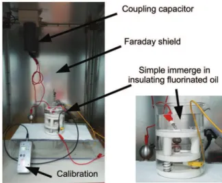
To confirm experimentally the efficiency at the triple point with the mesa structure, Partial Discharge (PD) measure-ments of machined substrate and conventional structure (Fig. 5) were performed. According on the IEC 60270 standard a PDIV (Partial Discharge Inception Voltage) measurement system is achieved. This system includes a power supply circuit, a coupling capacitor, a high voltage probe. The sample is placed between two balls and immersed in an insulating fluorinated liquid (Galden HT55 solvay). All these elements are put into a closed cupboard for electrical safety and also to reduce electro-magnetic noise (Fig.15). The measurements of the PDIV and the intensity of PD were carried out under sinusoidal voltage of 50 Hz. The applied Vrms voltage is increased manually in successive steps.
For 8 samples without mesa and 8 with a mesa struc-ture, results are shown in Figure16, for partial discharges detection voltages at 10 pC (P DDV10pC). The RMS
volt-age avervolt-age of the P DDV10pCis 7 kV for samples without
mesa and 9.2 kV for structures with a mesa, which corre-sponds to a significant gain of +30%. The larger dispersion of the P DDV10pCvalues for the machined samples might
be associated to the machining of copper (as observed for example in Fig. 13, showing “protuberance” at the copper surface edge), or to the greater surface rough-ness after machining at the bottom of the mesa (shown in Fig. 14). Both could contribute to the dispersion of values for machined samples. The P DDV10pC results are
less diffused for structure without mesa, it being caused by a different and probably simple origin, related to the shape of the bottom of the copper metallization where the electric field is reinforced.
Fig. 16. Partial discharge detection voltage at 10 pC for sample
immersed in an insulating liquid (Galden HT55 solvay) with or without mesa.
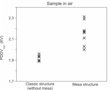
Fig. 17. Partial discharge detection voltage at 10 pC for sample
in air with or without mesa.
The measurements were repeated in other insulating liquids (Fluorinert FC-72 and Novec 649, 3M) and in the air and also for different detection levels (1 pC, 5 pC) with always a gain in terms of the threshold voltage of appearance of DP, associated with the mesa structure. The example of the results of the measurements made in the air is presented in Figure17.
These results are encouraging, since in a real encap-sulated system, at the areas of maximum stress (triple points) will not necessarily be localized at the most favor-able areas for defects (i.e. air bubbles, encapsulation voids). Defects are more likely to form at the foot of the reliefs during the implementation of the encapsulation. Thus, from the point of view of partial discharges, the mesa structure should make it possible to increase their
In this work we have investigated a new geometric struc-ture to reduce the electric field intensity at a singular point, the triple point in the power module. By the means of the FEM analysis, we have compared conventional and mesa structures and we have obtained a signifi-cant improvement. The mesa structure is implemented by an ultrasonic machining technique, to ensure align-ment of the flanks between ceramic and copper. Even if the machining introduces imperfections, the measure-ments carried out make to obtain an improvement of electrical results for partial discharges tests compared to the conventional structure. Moreover, the substrate struc-ture proposed here offers perspectives to be combined with other technologies, such as employing innovative encapsulating materials, in order to cumulate their effects to diminish the electrical stress at the triple point.
Author contribution statement
H. Hourdequin and M-L. Locatelli conceived of the pre-sented idea; M-L. Locatelli, P. Bidan, and L. Laudebat were involved in supervising the project. H. Hourdequin, L. Laudebat and M-L. Locatelli carried out the elec-trical experiments. H. Hourdequin, L. Laudebat and P. Bidan, performed FEM simulations. Z. Valdez-Nava con-tributed to the choice of implementation techniques. All authors contributed to the interpretation of the results. L. Laudebat took the lead in writing the manuscript. L. Laudebat and M-L. Locatelli wrote the manuscript with input from all authors. All authors discussed the results and contributed to the final manuscript.
Open Access This is an open access article distributed under the
terms of the Creative Commons Attribution License (http:// creativecommons.org/licenses/by/4.0), which permits unre-stricted use, distribution, and reproduction in any medium, provided the original work is properly cited.
References
1. Y. Developpement, Power module packaging –
mate-rial market and technology trends 2017, www.yole.fr
(2017)
2. T. Kimoto, K. Kawahara, H. Niwa, N. Kaji, J. Suda, Ion implantation technology in SiC for power device applica-tions, in International Workshop on Junction Technology
(IWJT) (2014) pp. 1–6
3. S. Ryu, C. Capell, C. Jonas, Y. Lemma, M. O’Loughlin, J. Clayton, E. Van Brunt, K. Lam, J. Richmond, A. Burk et al., Ultra high voltage IGBTs in 4H-SiC, in 1st Workshop
on Wide Bandgap Power Devices and Applications (2013),
pp. 36–39
4. S. Madhusoodhanan, K. Hatua, S. Bhattacharya, S. Leslie, S.H. Ryu, M. Das, A. Agarwal, D. Grider, Comparison study of 12 kV n-type SiC IGBT with 10kV SiC MOSFET
H. Hourdequin et al.,: Eur. Phys. J. Appl. Phys. 87, 20903 (2019) 11
and 6.5kV Si IGBT based on 3L-NPC VSC applications, in Energy Conversion Congress and Exposition (ECCE) (IEEE, 2012), pp. 310–317
5. H. Miyake, T. Okuda, H. Niwa, T. Kimoto, J. Suda, IEEE Electr. Device Lett. 33, 1598 (2012)
6. H. Masafumi, I. Yuji, I. Yoshinari, Packaging technologies
for SiC power modules, Fuji Electric Review (2012)
7. L. M´enager, B. Allard, V. Bley, Conditionnement des
mod-ules de puissance, Techniques de l’ing´enieur ´Electronique de puissance: conversion et gestion (2010)
8. CREE, Sic custom power services, www.wolfspeed.com
(2017)
9. T. Negishi, R. Tsuda, K. Ota, S. Iura, H. Yamaguchi, 3.3-kV All-SiC Power Module for Traction System Use, in
International Exhibition and Conference for Power Elec-tronics, Intelligent Motion, Renewable Energy and Energy Management (PCIM Europe, 2017), pp. 1–6
10. H. Hourdequin, PhD thesis, Toulouse University, 2018 11. N. Wang, I. Cotton, J. Robertson, S. Follman, K. Evans,
D. Newcombe, IEEE Trans. Dielectr. Electr. Insul. 17, 1319 (2010)
12. J. Zhou, S. Ang, A. Mantooth, J.C. Balda, A nano-composite polyamide imide passivation for 10 kV power electronics modules, in Energy Conversion Congress and
Exposition (ECCE) (2012) 4262–4266
13. G. Mitic, T. Licht, G. Lefranc, IGBT module technology with high partial discharge resistance, in Conference Record
of the 2001 IEEE Industry Applications Conference. 36th IAS Annual Meeting (2001), Vol. 3, pp. 1899–1904
14. L. Donzel, J. Schuderer, IEEE Trans. Dielectr. Electr. Insul.
19, 955 (2012)
15. M. Kozako, Z. Valdez-Nava, S. Diaham, S. Dinculescu, T. Lebey, Fundamental investigation of dielectric phenom-ena in epoxy composites during curing process under a uniform electric field, in Annual Report Conference on
Elec-trical Insulation and Dielectric Phenomena CEIDP (2012),
pp. 574–550
16. G. Belijar, S. Diaham, Z. Valdez-Nava, T. Lebey, J. Phys. D: Appl. Phys. 49 (2016)
17. S. Diaham, Z. Valdez-Nava, L. Leveque, G. Belijar, L. Laudebat, T. Lebey, Method for processing an elec-trically insulating material providing same with self-adjusting electric field grading properties for electrical
components, in International Patent PCT/EP2017/063740,
CNRS/UPS/INUC, 6 June 2017, PCT/EP2017/063740
18. L. Leveque, PhD thesis, Toulouse University, 2017
19. M.T. Do, PhD thesis, Joseph-Fourier University - Grenoble I, 2008
20. D. Frey, J. Schanen, J. Auge, O. Lesaint, Electric field investigation in high voltage power modules using finite element simulations and partial discharge measurements, in 38th IAS Annual Meeting on Conference Record
of the Industry Applications Conference (2003), Vol. 2,
pp. 1000–1005
21. H. Reynes, C. Buttay, H. Morel, Protruding ceramic sub-strates for high voltage packaging of wide bandgap semicon-ductors, in 5th Workshop on Wide Bandgap Power Devices
and Applications (WiPDA) (2017), pp. 404–410
22. G. Betti Beneventi, M. DalRe, L. Vincetti, Adv. Electro-magn. 7, 53 (2018)
23. C. Bayer, E. Baer, U. Waltrich, D. Malipaard, A. Schletz, IEEE Trans. Dielectr. Electr. Insul. 22, 257 (2015)
24. H. Hourdequin, L. Laudebat, M.L. Locatelli, P. Bidan, Design of packaging structures for high voltage power elec-tronics devices: Electric field stress on insulation, in
Interna-tional Conference on Dielectrics (ICD) (2016), pp. 999–1002
25. M.L. Griffith, J.W. Halloran, J. Am. Ceram. Soc. 79, 2601 (2005)
26. U. Lakshminarayan, S. Ogrydiziak, H. Marcus, Selective Laser Sintering of Ceramic Materials, in International
Solid Freeform Fabrication Symposium (University of Texas,
1990), pp. 16–26
27. N. Travitzky, A. Bonet, B. Dermeik, T. Fey, I. Filbert-Demut, L. Schlier, T. Schlordt, P. Greil, Adv. Eng. Mater.
16, 729 (2014)
28. M. Goetz, N. Kuhn, B. Lehmeier, A. Meyer, U. Voller, Comparison of Silicon Nitride DBC and AMB Substrates for Different Applications in Power Electronics, in Power
Electronics Conference PCIM (2013), Vol. 1, pp. 57–65
29. A. Miric, P. Dietrich, H. Germany, Inorganic substrates for
power electronics applications (Heraeus Group, 2015)
30. P. Laurens, C. Dubouchet, D. Kechemair, Application des
lasers aux traitements de surface (Techniques de l’ing´enieur: Ma´eriaux, 1996)
31. M. Decup, PhD thesis, Toulouse University - Toulouse III, 2010
Cite this article as: H´el`ene Hourdequin, Lionel Laudebat, Marie-Laure Locatelli, Zarel Valdez-Nava, Pierre Bidan, Metallized ceramic substrate with mesa structure for voltage ramp-up of power modules, Eur. Phys. J. Appl. Phys. 87, 20903 (2019)