Publisher’s version / Version de l'éditeur:
Proceedings of the Conference Glass Performance Days, 2009-06
READ THESE TERMS AND CONDITIONS CAREFULLY BEFORE USING THIS WEBSITE. https://nrc-publications.canada.ca/eng/copyright
Vous avez des questions? Nous pouvons vous aider. Pour communiquer directement avec un auteur, consultez la
première page de la revue dans laquelle son article a été publié afin de trouver ses coordonnées. Si vous n’arrivez pas à les repérer, communiquez avec nous à [email protected].
Questions? Contact the NRC Publications Archive team at
[email protected]. If you wish to email the authors directly, please see the first page of the publication for their contact information.
NRC Publications Archive
Archives des publications du CNRC
This publication could be one of several versions: author’s original, accepted manuscript or the publisher’s version. / La version de cette publication peut être l’une des suivantes : la version prépublication de l’auteur, la version acceptée du manuscrit ou la version de l’éditeur.
Access and use of this website and the material on it are subject to the Terms and Conditions set forth at
The next generation of switchable glass : the micro-blinds
Lamontagne, Boris; Barrios, Pedro; Py, Christophe; Nikumb, Suwas
https://publications-cnrc.canada.ca/fra/droits
L’accès à ce site Web et l’utilisation de son contenu sont assujettis aux conditions présentées dans le site LISEZ CES CONDITIONS ATTENTIVEMENT AVANT D’UTILISER CE SITE WEB.
NRC Publications Record / Notice d'Archives des publications de CNRC:
https://nrc-publications.canada.ca/eng/view/object/?id=6c7d2744-b6af-47fd-9a51-9b5c6a2f48ad
https://publications-cnrc.canada.ca/fra/voir/objet/?id=6c7d2744-b6af-47fd-9a51-9b5c6a2f48ad
637 GLASS PERFORMANCE DAYS 2009 | www.gpd.fi
The next generation of switchable glass : the
Micro-Blinds
Boris Lamontagne1, Pedro Barrios1, Christophe Py1 and Suwas Nikumb2
1 Institute for Microstructural Sciences, National Research Council, Ottawa, Canada, K1A OR6 2 Industrial Materials Institute, National Research Council, London, Canada, N6G 4X8
Keywords
1=Switchable glass 2=smart windows 3=transmission 4=electrostatic actuator
Abstract
Switchable glass or smart windows have been developed and discussed for decades. They have bright futures in applications such as vehicle, architecture, privacy and energy efficient glazing among others. The existing technologies seriously suffer from customer acceptance. The next generation of switchable glass based on micro-blinds might help the incursion of smart windows to the market, or at least to some niche markets.
The micro-blinds are composed of invisible and electrostatically activated curling electrodes of 100 micrometers size. They can be deposited on flat glass by magnetron sputtering like regular low-E coatings, and then patterned by laser. They possess several advantages such as switching speed, UV durability, customized appearance and transmission, and do not employ costly ITO, relative to the current smart windows technologies: electrochromic, suspended particles and liquid crystals. Several groups have successfully developed curling electrodes for small area devices; the novelty of the proposed technology lies in the revolutionary and cost-effective processing scheme for large areas. This paper presents the status of our R&D project.
Introduction
Smart windows are characterized by variable or controllable transmission of the light through them. Various types of smart windows have been developed for over two decades. Some technologies reached the market, for example, Ferrari’s sunroof, Boeing’s Dreamliner windows or Velux’s skylight. However, for your house, would you pay 3 times the price of a regular skylight to be able to vary the transmission with pinholes and an on/off switching time of 10 min ? [1] In the literature, a lot of effort has been devoted on improving various existing technologies of smart windows; several hundred patents have been issued on electrochromism only. The performance of existing smart windows are very interesting, but not attractive enough to reach a large public, most
probably due to some weaknesses such as cost, speed, appearance (tint) and range of transmission.
This paper presents the next generation of switchable glazing, based on micro-blinds [2]. They are not related to any previous work on internal macroscopic Venetian blinds [3-4]. The micro-blinds are really of micrometer size; this makes them practically invisible to the eye. They are curling electrodes activated by voltage. Smart windows based on suspended particles use voltage to align mobile needles, while the micro-blinds use voltage to unroll curled electrodes and thus block the light transmission. Figure 1 shows such curled electrodes: micro-blinds.
Such curling electrodes have already been developed and tested successfully by several groups [5-10] on small areas (1-10 cm2) using standard
semiconductor fabrication techniques. Moreover some patents [11-13] have been issued to other groups for similar rolling electrodes. These devices were developed for electronic (switches), optical (small visor or display) and biological applications. Such devices could be considered a type of Micro Electro Mechanical Systems (MEMS), some of which have reached commercial applications all around us (inkjet printers, cars (airbags, gyroscopes, tire pressure sensors), DLP projectors, etc). For example, some Digital Light
Processing (DLP) projectors have millions of complex and tiny micro-mirrors activated by electrostatic forces. IMEC (Leuven, Belgium) recently presented a monolithically integrated 11 megapixel micro mirror array [14-15].
This paper presents a new application for the curled electrodes: smart
windows. The main novelty is the proposed fabrication scheme making their manufacturing feasible and cost-efficient on large areas by using laser processing, instead of standard microelectronic techniques.
Fabrication
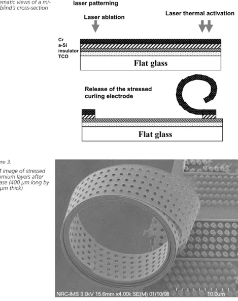
The fabrication process was designed to be performed on flat glass (large area), but it could also be applied to roll-to-roll manufacturing [2]. Figure 2 presents schematics of the cross-section of a micro-blind and illustrates some of the components and fabrication steps.
The first fabrication steps involve thin film deposition using common flat glass techniques like Chemical Vapor Deposition (CVD) or magnetron sputtering. The first layer could be any Transparent Conductive Oxide (TCO) such as SnO2:F; i.e. any typical low-emissivity layer or TCO without the requirement of flow transmission of infrared wavelengths. Contrary to other smart windows technologies such as electrochromism, our micro-blinds
Figure 1.
SEM image of partially curled micro-blinds
Challenges of L
arge Area Coating P
638 GLASS PERFORMANCE DAYS 2009 | www.gpd.fi are voltage driven, not current driven;
thus the micro-blinds do not require low resistivity film such as the expensive Indium Tin Oxide (ITO) layer. For our proof-of-concept, we use regular low-emissivity glazing such as PPG SunGate 500TM or Solarban 60 TM. A thin
dielectric is then deposited followed by a sacrificial layer. Finally the stressed layer is deposited. There are numerous possibilities for the layers, in our case we use amorphous silicon for the sacrificial layer and chromium for the stressed layer. Inorganic materials have been preferred to obtain good UV durability. There are different techniques to control the intrinsic stress in the curling layer. Our proof-of-concept device has a stress layer consisting of tensile and compressive chromium deposited by magnetron sputtering. The stress level is simply controlled by varying the Ar pressure during sputtering of the Cr. Figure 3 shows a test device (coil, not a micro-blind) consisting of 8 turns of the stressed layer. We have obtained stressed rolls of radius of curvature as small as 3 µm.
As mentioned before, one of the novelty of the micro-blinds is the use of laser processing to define their geometry allowing manufacturing on large area without contact. Laser thermal anneal activates the intermixing of the sacrificial layer and the stress layer, thus forming an anchor and etch stop (for the release process). Similar laser annealing of amorphous silicon has been developed for displays [16]. A laser ablation step defines the opening to release the curled micro-blinds. The proof-of-concept device has been fabricated by conventional lithography and etching methods, but laser tests were performed on the layers as shown in Figure 4 and 5. Figure 4 shows an oblique SEM view of a laser ablation of the sacrificial and stress layer.
The thin film deposited samples were mounted on a computer controlled CAD/CAM driven motion stage with vacuum hold-down fixture. Patterning of the coated thin film was carried out by the X-Y motion stage, which had a linear positioning accuracy of 1 µm. The processing feed rate was maintained at 5-10 mm/min. The experiments were performed in air using a Spectra-Physics Model:YHP40-532 nanosecond pulsed laser system, which delivered 30 ns pulses with an average power of 1 W at a wavelength of 532 nm and with pulse repetition rate of 1 kHz. After collimation with an 8X beam expander, the laser beam was focused using an f/50 mm lens. During experiments the ablation width was varied from 4µm to 9 µm for repetition rate of 500 and 1000 Hz. The laser fluence incident on the samples was controlled using a set of neutral density filters. The laser focal spot was also slightly defocused to avoid damage to the Si layer and to adjust the ablation track width the diode current was monitored. Although in these experiments, the
patterned lines are relatively rough, much smoother line shape could be obtained by using smaller spot size and by optimizing other conditions such as the spot overlap of the laser beam. Line edge roughness smaller than 1 µm have been obtained for the ablation of ITO [17]. Figure 5 shows a cross-sectional SEM view of the ablated layers. It shows various layers and points out only the stressed and sacrificial layers were ablated, not the layers underneath.
The next processing step (which could be performed at the Insulated Glass Unit (IGU) manufacturing site) is the release of the micro-blinds by etching the sacrificial layer. Wet or dry etching could be used. Dry etching using fluorocarbon plasma chemistry was preferred as it is clean and fast. Then the samples are ready for electrical actuation.
Results
Once the micro-blinds are released on the proof-of-concept devices (10 cm2
square glass pieces) electrical testing was performed. Actuation voltages as low as 20-30 V have been observed. Closing (roll-down) delay of the order of the ms is typical (in agreement with other types of curling electrodes [5-9].
Fabrication
Flat glass
Thin film deposition and laser patterning
Laser ablation
Flat glass
Release of the stressed curling electrode
Laser thermal activation
Cr a-Si insulator TCO
Figure 2.
Schematic views of a mi-cro-blind’s cross-section
Figure 3.
SEM image of stressed chromium layers after release (400 µm long by 0.1 µm thick)
Figure 4.
Chromium and amorphous silicon layer ablated by laser
Figure 5.
SEM cross-sectional view pointing out that the ablation only affected the Cr and a:Si layers
Challenges of L
arge Area Coating P
639 GLASS PERFORMANCE DAYS 2009 | www.gpd.fi
Opening (roll-up) delay seems a slightly longer, but still below one second.
Visual appearance can be neutral, there is no strong unappealing tint such as observed on other types of smart windows. The weak tint is related to the TCO layer and can be very minimal. Moreover, the appearance in the open and closed state can be customized to the choice of the user. Haze or scattering is minimal, probably similar to the Suspended Particles Devices (SPD) technology. Since micro-blinds are made of inorganic and high temperature melting materials, they are very resistant to temperature variations.
More work in underway to get a better understanding of the behavior and solving several open issues (materials science, electrostatic, etc).
Discussion
The micro-blinds are a new idea for smart windows. They are following extensive work from several groups on curling switches or actuators [5-9] proving their reliability. The use of laser processing could make them cost-efficient for smart windows. There is still considerable amount of work to be done to prove their manufacturing feasibility on large areas. Nevertheless, laser patterning is a sector developing rapidly and of great interest for the flat panel display industry. Moreover, current FPD techniques like projection lithography could also be used to fabricate micro-blinds but with a cost limiting the sector of application.
The micro-blinds have a great potential to attract end-users, their expected performances compare very well with the other existing technologies for smart windows, as illustrated in table 1.
The predicted characteristics of the micro-blinds compare very well with the measured ones from the other technologies of smart windows. Note that we did not include the liquid crystals since they are mainly oriented toward partitions or interior privacy applications, while the micro-blinds require double glass panels such as the IGUs.
In case of power failure, the micro-blinds would go in open state, contrary to the SPD (safety hazard). SPDs and rolling electrodes (micro-blinds) are expected to have remarkable low power consumption of approximately 1 W/m2 [20]. Both SPD and EC smart
windows are characterized by very low UV transmission (<1%), the micro-blinds in the opaque state could also have very low UV transmission. However, contrary to the existing technologies, the micro-blinds could be designed if requested to have a notable UV transmission to the benefit of the occupant’s health. The lack of UV exposure in our environment (work, house, school, etc) has been identified as a possible cause of Sick Building Syndrome (SBS)[22]. Reduced fading of colors induced by UV and visible on fabrics like curtain does not seem a very good selling argument, compared to the occupant’s health.
Smart windows have the potential to reduce the glare, improve privacy (increase the comfort of the occupant) as well as save energy [22]. Reducing cooling load (opaque) and automatized –optimized daylighting are two major ways to save energy. Moreover, two unique characteristics of the micro-blinds make them even more attractive for energy savings: they are not opaque but are reflective (better thermal performances), and have a higher solar transmittance range (suitable for passive solar heating).
Conclusions
Micro-blinds are a new type of smart windows based on stressed curling electrodes actuated by electrostatic forces. They possess several favorable characteristics (speed, cost, durability, appearance, etc) giving them a bright future. More work is needed to prove their reliability and laser manufacturability.
References
[1] www.veluxusa.com
[2] B. Lamontagne and C. Py, Microblinds and a method of fabrication thereof, Patent application US 2006/0196613
[3] S.F. Kiefer, L. M. Silverberg and M.L. Gonzalez, Electrostatically actuated window blinds, J. Electrostatics 50, 229, 2001
[4] M.P. Butterfield, Design and manufacture of a second generation switch-operated window wall, thesis, North Carolina State University, 2006.
[5] S. Goodwin-Johansson, M. Davidson, D. Dausch, P.H. Holloway and G. McGuire, High speed, large motion electrostatic artificial eyelid, IEEE conference on MEMS, p.610, 2002. [6] S.H. Goodwin, D.E. Dausch, S.L. Solomon
and M.K. Lamvik, Electrostatic artificial eyelid actuator as an analog micromirror device, Proc. SPIE 5785, p.59, 2005
[7] S.H. Goodwin-Johansson, M.R. Davidson, D.E. Dausch, P.H. Holloway and G. McGuire, Proc. SPIE 4695, p.451, 2002.
[8] M. Pizzi, V. Koniachkine, M. Nieri, S. Sinesi and P. Perlo, Electrostatically driven film light modulators for display applications, Microsystem Technologies 10, 17, 2003 [9] P. Roux, E. Woirgard, M. Pizzi, O. de Martiis
and V. Koniachkine, Fem modeling of an electro-optical micro-shutter, Sensors Actuators A119, 1, 2005.
[10] J. den Toonder et al., Artificial cilia for active micro-fluidic mixing, Lab Chip 8, 533, 2008. [11] C.G. Kalt, Electro-static device with rolling
electrode, US patent 3,989,357
[12] G.R. Simpson, Light control device, US patent 4,248,501
[13] C.O. Bozler and S. Rabe, Spatial light modulator, US patent 5,784,189
[14] www.micronanosystems.info, Newsdesk p. 26, January 2009
[15] IMEC Newsletter 55, p.1, 2009 (also available on the web)
[16] T. Arai, N. Morosawa, Y. Hiromasu, K. Hidaka, T. Nakayama, A. Makita, M. Toyota, N. Hayashi, Y. Yoshimura, A. Sato, K. Mamekawa, Y. Inagaki, N. Umezu and K. Tatsuki, Micro Silicon Technology for Active Matrix OLED Display, SID 07 Digest, 1370, 2007. [17] N. Fukuda, K. Kunishio and S. Nakayama,
Dry-etching system with Q-switched DPSS Laser for Flat Panel Displays, J. Laser Micro/Nanoeng. 2, 241, 2007.
[18] www.sage-ec.com [19] www.refr-spd.com
[20] J. Rostron Ed., Sick Building Syndrome, Spon Press, 1998.
[21] N. Baker and K. Steemers, Daylight Design of buildings, Earthscan publications, 2001. [22] J. Karlsson, Control system and energy saving
potential for switchable windows, IBPSA conference, p.199, 2001.
Parameters Electrochromism (18)
Suspended particles
(19) Micro-blinds
Transm. visible max 62% 50% ~65%
Transmission solar range
30% 30%
~60% Appearance Yellow-blue Neutral,Blue tint Neutral, custom Speed Slow (1-10 min) Fast ( few seconds) Ultrafast (ms) Operation voltage 1-5 V 50-120 V 30-50 V UV resistance Good Good Excellent Temperature
operating range Approx. -30 ° to 70° C -40° to 100°C Very wide ~-50° to 300° C
Table 1
Comparison of perform-ances Micro-blinds vs existing technologies for smart windows
Challenges of L
arge Area Coating P