A BODY AREA NETWORK FOR WEARABLE HEALTH
MONITORING: CONDUCTIVE FABRIC GARMENT UTILIZING
DC-POWER-LINE CARRIER COMMUNICATION
by Eric R. Wade
S. B. Mechanical Engineering
Massachusetts Institute of Technology, 2000 S. M. Mechanical Engineering
Massachusetts Institute of Technology, 2004 S. M. Electrical Engineering
Massachusetts Institute of Technology, 2004 Submitted to the Department of Mechanical Engineering in Partial Fulfillment of the Requirements for the Degree of
Doctor of Philosophy in Mechanical Engineering at the
Massachusetts Institute of Technology February 2007
© 2007 Massachusetts Institute of Technology All rights reserved
Signature of Author ………... Department of Mechanical Engineering January 12, 2007 Certified by ………...………
H. Harry Asada Ford Professor of Mechanical Engineering Thesis Supervisor Accepted by ………...
Lallit Anand Chairman, Department Committee on Graduate Students
A Body Area Network for Wearable Health Monitoring: Conductive Fabric Garment utilizing DC-Power-line Carrier Communication
by Eric R. Wade
Submitted to the Department of Mechanical Engineering On January 12, 2007 in Partial Fulfillment of the Requirements of the Degree of Doctor of Philosophy in
Mechanical Engineering ABSTRACT
Wearable computing applications are becoming increasingly present in our lives. Of the many wearable computing applications, wearable health monitoring may have the most potential to make a lasting positive impact. The ability to remotely monitor physiological signals such as respiration, motion, and temperature has benefits for populations such as elderly citizens, fitness professionals, and soldiers in the battlefield. To fully integrate wearable networks into a user’s daily life, these systems must be minimally invasive and minimally intrusive. At the same time, such wearable networks require multiple sensors and electronic components to be mounted on the body. Unfortunately, typical off-the-shelf components of this nature are heavy, bulky, and don’t integrate well with the human form. Thus, it is critical to figure out how best to minimize the physical and mental burden that these systems place on the user.
To address these problems, we propose a new method of designing wearable health monitoring networks by combining electrically conductive fabrics and power-line communication technology. Electrically conductive fabrics are useful in that they feel and behave like normally worn clothing but also have the ability to transmit data and power. To fully exploit the conductive fabric as a transmission medium, we also use power-line communication technology. Power-line communication allows for simultaneous power and data transmission over a shared medium. The use of these two technologies will allow us to significantly reduce the amount of metal cabling on the body and to reduce overall system bulk and weight.
With this project, we design the DC-PLC system that will act as the physical layer of the architecture. Next, we construct a prototype body area network, and derive analytical models for predicting garment electrostatic and electro-dynamic properties using Maxwell’s equations, and verify using empirical data and finite-element analysis. Finally, we will determine relevant rules and guidelines for the design and construction of such garments.
Thesis Supervisor: H. Harry Asada
I would like to thank God for using me as his instrument. This work is a manifestation of His will and power. I dedicate this work to all of those who have played a part in getting me to this point in my life, most especially; my parents, Jerome and Leslie; my brothers, Jerome, Neil and Craig; and Mikii, without whom none of this would have been possible.
TABLE OF CONTENTS
1. INTRODUCTION 10
1.1. WEARABLE HEALTH MONITORING 10
1.2. COMMUNICATION OVER DCPOWER-LINES 11 1.3. CONDUCTIVE FABRIC SIGNAL TRANSMISSION 13
1.4. SYSTEM INTEGRATION 14
2. WEARABLE HEALTH MONITORING 16
2.1. THE NEED FOR WEARABLE HEALTH MONITORING 16
2.2. TRADITIONAL HEALTH MONITORING TECHNIQUES 17
2.3. CHALLENGES OF HEALTH MONITORING 19
2.4. OUR SOLUTION:DC-PLC USING CONDUCTIVE FABRICS 20
2.4.1. Addressing existing problems 20
2.4.2. Accommodating wearability metrics 21
3. DC POWER-LINE CARRIER COMMUNICATION 23
3.1. DCPOWER-LINE COMMUNICATION NETWORK 24
3.1.1. Architecture 24
3.1.2. Technical Issues 25
3.2. MODEM DESIGN AND ANALYSIS 25
3.2.1. Hardware Requirements and Problems 25 3.2.2. Use of Transmission Line Transformer 27
3.2.3. TLT Modeling 28
3.2.4. System Performance 30
3.2.5. High Fanout Design Protocol 34
3.3. IMPLEMENTATION AND EXPERIMENTS 35
3.3.1. Prototype 35
3.3.2. Design 36
3.3.3. Experimental Evaluation 37
4. ELECTROMAGNETISM IN CONDUCTIVE FABRICS 41
4.1. ELECTROMAGNETIC WAVES ON CONDUCTIVE FABRICS 41
4.2. 2DBEHAVIOR 44
4.2.1. Electrostatic Analysis 45
4.2.2. Verification of Homogeneity 46
4.3. OHMIC CONDUCTION 47
5. DC ANALYSIS OF CONDUCTIVE FABRICS 51
5.1. 1D AND 2DCONDUCTIVITY 51
5.2. DERIVING THE CLOSED-FORM 3DSOLUTION 52
5.2.1. Cylindrical Reduction 52
5.2.2. Resistivity of Cylinders 53
5.3. 3DPREDICTION METHOD 54
6. AC ANALYSIS OF CONDUCTIVE FABRIC 60
6.1. DESIGN CHALLENGES 60
6.1.1. Bandwidth and Gain 60
6.1.2. Transient Behavior 61
6.1.3. Noise and interference 61
6.2. INITIAL TESTS AND EXPERIMENTATION 62
6.2.1. Bandwidth 62
6.2.2. Impedance matching 64
6.3. TRANSMISSION LINE THEORY 65
6.4. DERIVING THE TLMODEL FOR OUR GARMENT 68
6.5. DERIVING TRANSMISSION LINE PARAMETERS 71
6.5.1. Wave number 71
6.5.2. Characteristic Impedance 72
6.5.3. Equivalent Length 77
6.6. SHOULDER SECTION 82
6.7. VERIFICATION 83
7. GARMENT FABRICATION AND PERFORMANCE TESTS 85
7.1. GARMENT FABRICATION 85
7.1.1. Electronic Circuit 88
7.2. PERFORMANCE TESTS 90
7.2.1. Garment shape 90
7.2.2. Effect of garment on transmission properties 91
7.2.3. Motion artifact 94
8. APPLICATIONS 96
8.1.1. Physical Construction 96
8.1.2. Sensor Shell and Physical Construction 97
8.2. CENTRAL-SIDE COMPONENTS 98
8.2.1. Electronic Circuit 99
8.4. SENSOR REMOVAL 100
8.5. BIOMECHANICAL MODEL RECONSTRUCTION 101
8.6. HUMAN ROBOT INTERACTION 103
9. CONCLUSION 105
10. APPENDICES 108
10.1. DERIVATIONS OF P3 LEADING TERM 108 10.2. DERIVATION OF ZT(S) 109
10.3. IMPEDANCE COEFFICIENTS 110
10.4. GAIN COEFFICIENTS 110
TABLE OF FIGURES
FIG.1CONDUCTIVE FABRIC GARMENT 10
FIG.2DC-PLCSYSTEM DIAGRAM 12
FIG.3SANDWICH SECTION CONSTRUCTION OF CONDUCTIVE FABRIC GARMENT 13 FIG.4SINGLE STRAND COMPARED TO A SHEET 14 FIG.5ILLUSTRATION OF RELATIVE MOTION OF ARM TO THE HIP AND THE EXTREME POINTS OF THE BODY
DURING THE WALKING GAIT 22
FIG.6ARCHITECTURE OF DC POWER BUS COMMUNICATION SYSTEM 24
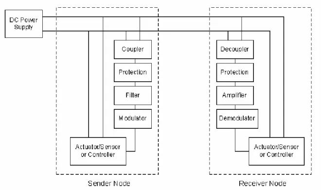
FIG.7BLOCK DIAGRAM OF DCBUS TRANSMISSION COMPONENTS 26
FIG.8STANDARD COUPLING/DECOUPLING CIRCUITRY 26
FIG.9BASIC BUILDING BLOCK FOR TRANSVERSE TRANSMISSION MODE CIRCUITS AND COUPLING AND DECOUPLING CIRCUITS WITH TRANSMISSION LINE TRANSFORMER 27 FIG.10 GUANELLA TRANSMISSION LINE TRANSFORMER MODEL ACCOUNTING FOR MAGNETIZING
INDUCTANCE AND WINDING RESISTANCE 29
FIG.11 IMPEDANCE OF TRANSMISSION LINE TRANSFORMER WITH TERMINATING RESISTOR 30
FIG.12 CIRCUIT DIVIDED INTO SECTIONS: SENDER SIDE COMPONENTS,CPS, RECEIVER SIDE COMPONENTS
31
FIG.13 IMPEDANCE AND GAIN AS A FUNCTION OF N 33
FIG.14 SIMPLIFIED CIRCUIT SCHEMATIC AND THE RESULTING EQUIVALENT CIRCUIT MODEL FOR LARGE N
34
FIG.15 TOP AND BOTTOM VIEWS OF PROTOTYPE MODEM 36 FIG.16 ORIGINAL TRANSMITTED DIGITAL SIGNAL AND RECEIVED SIGNAL 38
FIG.17 SIGNAL TRANSMISSION IMPEDANCE VIEWED FROM SENDER FOR N=1, A SINGLE NODE, AND N=30,
THIRTY NODES 39
FIG.18 PEAK MAGNITUDE AND FREQUENCY 40
FIG.19 CONDUCTIVE FABRIC GARMENT WITH SENSOR NODES EMBEDDED AT VARIOUS POINTS 42
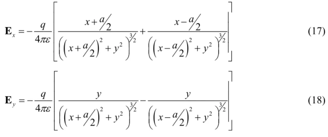
FIG.20 FIELD LINES AND EQUIPOTENTIALS DUE TO AN ELECTRIC DIPOLE 43
FIG.21 CONDUCTIVE SHEET USED FOR ELECTROSTATIC MODELING 45 FIG.22 MEASURED RESISTANCE AND MODEL RESISTANCE FOR SHEET 47
FIG.23 STRIP OF CONDUCTIVE FABRIC WITH A POINT OF TRANSMISSION AND A POINT OF RECEPTION 47
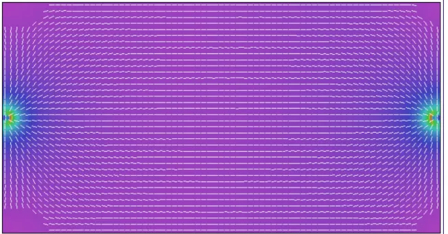
FIG.24 FINITE ELEMENT REPRESENTATION OF FIELD LINES IN A CONDUCTIVE FABRIC STRIP 48
FIG.25 FINITE ELEMENT REPRESENTATION OF FIELD LINES IN A SQUARE CONDUCTIVE FABRIC STRIP. 49
FIG.26 THE CONDUCTIVE FABRIC GARMENT AS A REPLACEMENT FOR THE CPS LINE OF FIG.12 50
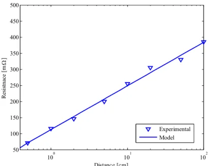
FIG.27 RESISTANCE OF SHEET AND THREAD VS.LENGTH 51
FIG.28 GARMENT SIMPLIFIED AS CYLINDRICAL SECTIONS AND CYLINDRICAL SECTION BEING
‘UNWRAPPED’ 53
FIG.30 PLOT OF RESISTANCE VS.DISTANCE FOR CYLINDERS OF DIAMETER 9,18, AND 36CM 54
FIG.31 PLOT OF RESISTANCE VS.DISTANCE FOR A CYLINDERS OF DIAMETER 9,18, AND 36CM 55
FIG.32 EQUIVALENT RESISTANCE DIAGRAM FOR GARMENT 56
FIG.33 COMPARISON OF EMPIRICAL AND PREDICTED RESISTANCE VALUES IN [MΩ] 57
FIG.34 FINITE ELEMENT CONSTRUCTION OF THE GARMENT AND CLOSE-UP VIEW OF THE SHOULDER
SECTION 57
FIG.35 OLD AND NEW PREDICTION METHODS FOR RESISTANCE VALUES ALONG THE ARMS 58 FIG.36 RESULTS OF REVISED PREDICTION METHOD 58 FIG.37 COMPARISON OF THE ORIGINAL PREDICTION METHOD AND THE REVISED PREDICTION METHOD
WHICH ACCOUNTS FOR SHOULDER GEOMETRY 59
FIG.38 DISTRIBUTED CAPACITANCE OF PARALLEL CONDUCTORS 61
FIG.39 GARMENT TRANSMISSION AND MEASUREMENT POINTS 62
FIG.40 SIGNAL AMPLITUDES AT 1MHZ AND 20.6MHZ TAKEN AT THE NECK AND WRIST 63
FIG.41 IMPEDANCE ANALYZER SETUP FOR MEASURING GARMENT IMPEDANCE 64
FIG.42 GAIN AND PHASE PLOTS FOR COMPLEX IMPEDANCE Z0(ω) FOR ENTIRE GARMENT 65
FIG.43 PARALLEL-PLATE TRANSMISSION LINE MODEL 66
FIG.44 TRANSMISSION LINE IMPEDANCES AND RESISTANCES 67
FIG.45 TRANSMISSION LINE APPROXIMATION OF THE CONDUCTIVE FABRIC GARMENT 68
FIG.46 PARAMETERS FOR DESCRIBING TRANSMISSION LINE APPROXIMATION OF THE GARMENT 69
FIG.47 MEASURING CONDUCTIVE FABRIC PERMITTIVITY 72 FIG.48 CYLINDRICAL SECTION WITH IDEAL TRANSMISSION CHARACTERISTIC AND ACTUAL
TRANSMISSION CHARACTERISTIC 73
FIG.49 CYLINDRICAL SECTION WITH SMA-TO-SOLDER-BOARD CONNECTION 74
FIG.50 CAPACITANCE AND INDUCTANCE VERSUS LENGTH FOR CYLINDRICAL CONDUCTIVE FABRIC
SECTIONS 75
FIG.51 CAPACITANCE AND INDUCTANCE PER UNIT LENGTH VERSUS DIAMETER 76
FIG.52 UNWRAPPING A CYLINDER FOR VISUAL REPRESENTATION 78
FIG.53 FIELD LINES IN A CONDUCTIVE FABRIC STRIP, WITH LINEAR REGION HIGHLIGHTED 78 FIG.54 TWO STRIPS OF EQUIVALENT IMPEDANCE; ONE WITH POINT PROBES, AND ONE WITH FULL-WIDTH
PROBES 79
FIG.55 TWO STRIPS OF EQUIVALENT IMPEDANCE, WITH LIKE REGIONS SHADED 79
FIG.56 MODEL AND EXPERIMENTAL RESULTS FOR A CYLINDER WITH D/L OF 0.167 80
FIG.57 EQUIVALENT LENGTH VERSUS ACTUAL LENGTH AND DIAMETER FOR CYLINDRICAL SECTIONS 81
FIG.58 FINITE ELEMENT MODEL OF SHOULDER USED FOR CAPACITANCE TESTS 82
FIG.59 IMPEDANCE CHARACTERISTIC FOR ARM AND TRUNK SECTIONS 83
FIG.60 IMPEDANCE FOR OPEN-CIRCUITED GARMENT 84 FIG.61 LAYERING OF CONDUCTIVE FABRIC AND INSULATION 86
FIG.62 METHOD FOR CONNECTING SENSOR NODES TO THE CONDUCTIVE FABRIC GARMENT 86
FIG.63 SEQUENCE FOR PLACING SENSORS ON GARMENT 87
FIG.64 TRANSMISSION SIDE OF DC-PLC CIRCUIT COMPONENTS 89
FIG.65 GARMENT ON MODEL, RESTING, AND CRUMPLED ON BENCH-TOP 90
FIG.66 IMPEDANCE CURVES FOR GARMENT ON THE MODEL, RESTING, AND CRUMPLED 91
FIG.67 PWM SENSOR OUTPUT DURING MOTION 92 FIG.68 DEMODULATED MOTION MEASURED DIRECTLY FROM THE SENSOR AND THROUGH THE GARMENT
93
FIG.69 ACCELEROMETER PWM SIGNAL DIRECTLY FROM SENSOR, AND MEASURED THROUGH THE
GARMENT 94
FIG.70 POSITION INFORMATION GAINED DIRECTLY FROM SENSOR, AND MEASURED THROUGH THE
GARMENT 95
FIG.71 SENSOR PCB AND PCB WITH COMPONENTS SOLDERED IN PLACE 97
FIG.72 SENSOR SHELL FOR OPEN SENSORS 98 FIG.73 SENSOR SHELL FOR CLOSED SENSORS 98 FIG.74 ISOLATING THE CF LAYERS FROM ONE ANOTHER AND THE ENVIRONMENT 100
FIG.75 SEPARATING THE SENSOR SHELL FROM THE GARMENT 100
FIG.76 ELASTIC STRIPS TO MINIMIZE MOTION AT THE WRIST 101
FIG.77 PARAMETERS FOR ARM HEIGHT MEASUREMENTS 101
FIG.78 INITIAL CALIBRATION RESULTS FOR ACCELEROMETER EXPERIMENTS 102
FIG.79 ACCELEROMETER AXES 103
FIG.80 ROBOT GAINING VISUAL INFORMATION FROM SENSORS EMBEDDED IN GARMENT 104
FIG.81 SHEET RESISTANCE 108
1. Introduction
1.1. Wearable Health Monitoring
In recent years, we have seen many advances in the field of wearable computing. Wearable computing is fast becoming a ubiquitous concept. Of the many wearable computing applications, wearable health monitoring will have an immense and immediate benefit to our quality of life by allowing for constant monitoring of physiological signals such as limb motion, respiration, and skin temperature. Such systems can expedite recovery and rehabilitation, immediately address a sudden decline in health, and assist those in need until they have access to a health professional. In order for this wearable network to be widely accepted, it must also be minimally invasive and minimally intrusive. Specifically, the users of such a system should be able to carry out their normal activities without actual or perceived impediment from the wearable network. The ideal users of such systems are fitness professionals [1],[2], soldiers in the battlefield [3],[4], and particularly the elderly population [5],[6]. The elderly population, often at increased risk for health problems, has been steadily increasing. Finding the facilities and resources for dealing with these problems is critical. Oftentimes, elderly people are forced to stay in a hospital or nursing home while physiological signals are monitored. With this work, such patients will be able to return to their homes for improved quality of life.
Many health monitoring applications require the placement of electrical components on the user. Placing these components on the body requires careful consideration for the physical connections of the components, the bulk and weight of the components, and the routing of wires along the body [7],[8]. For instance, locations of minimum movement and maximum load carrying capacity are optimal for locating heavy components, and should be considered for the design of these systems [9]. In fact, numerous metrics for wearability have been discussed, but are not often implemented.
The authors have devised a unique approach to addressing these issues by applying direct-current power-line carrier communication (DC-PLC) technology to a wearable monitoring system. DC-PLC is a technology in which a single shared DC bus is used to provide power to each node and facilitate communication between multiple nodes in an electrical network [10]. In our system, sensor nodes are embedded in the garment at various locations. The sensor nodes transmit data to a master node which transmits all sensor information wirelessly to a local capture and storage medium, such as a personal computer.
To truly make the system wearable and to allow for connectivity of sensors at any point on the body, we must ensure that the DC bus is flexible and lightweight, which precludes the use of traditional metal wiring. Instead, we propose to use conductive fabric sheets sewn into clothing garments as the electrical transmission medium, as demonstrated in [11] and [12]. These fabrics do not restrict the wearer’s body movement and behave like normal fabrics. Initial work on the use of conductive fabric sheets for electrical transmission has been conducted by the authors as well as others [12],[13],[14].
1.2. Communication over DC Power-lines
Simultaneous transmission of power and information over a single medium is commonly known as power-line carrier communication, or simply power-line communication (PLC). This technology has been used primarily for in-home networks to transmit data over pre-laid power lines. However, we propose to use PLC over a conductive fabric garment for a localized, body-area network. Thus, our network architecture is different from these pre-existing systems.
The direct current (DC) PLC system, pictured in Fig. 2, was first introduced and applied to a wearable system in [11]. In [10], the authors described an implementation for
such a system that relies on transmission-line transformer (TLT) theory and knowledge of the medium’s resistive properties to minimize insertion losses associated with PLC transformers. The DC-PLC system consists of three components; the transmission medium, a master command node, and the sensor nodes. The system we have developed requires only two conductors; a supply line, that we call the consolidated power-signal (CPS) line, and a ground line for electrical return. The CPS is used to transmit both DC power and data between the master node and the sensor nodes within the system. The master node acts as the command node by sending commands to and reading data from the sensors located throughout the network. It also contains a single battery which serves as the power source for the system. As a result, the sensors do not need local batteries; this reduces the overall bulk and weight of the network. As the number of sensor nodes increases, these savings become more significant.
Fig. 2 DC-PLC System Diagram
We must allow for connectivity of multiple types of sensors to gather a variety of physiological signals. Therefore, we need a means of converting the DC battery voltage of the master node to each sensor’s required power level. Similarly, we need to convert the sensor outputs to a digital signal. A modem is needed to perform these functions. The sensor nodes utilize a modem developed by the authors specifically for a high-fanout DC-PLC system [10]. The modem, which contains a DC-to-DC converter, an analog-to-digital converter, a TLT, and a phased-lock loop, can be interfaced with a multitude of sensor types. It can read both analog and digital data, then digitize (if necessary), encode, and modulate the signal for transmission over the CPS to the master node. Frequency-shift keying (FSK) is used to modulate the signals, and frequency separation is used to minimize the number of collisions between sensor node transmissions. Each sensor is
assigned a specific carrier frequency; when the master node wants to view data from a given sensor, it demodulates the aggregate signal seen on the power line using the appropriate carrier.
Our prototype is pictured in Fig. 1. We construct the garment with a ‘sandwich’ of conductors and insulators, as shown in Fig. 3. There are two layers of conductive fabric, one each used for transmission and grounding. In addition, there are three layers of insulation to prevent electrical contact between the ground and supply lines, between ground and the environment, and between supply and the user.
Conductive Fabric Insulation
Fig. 3 Sandwich Section Construction of Conductive Fabric Garment
1.3. Conductive Fabric Signal Transmission
The CPS and ground line are constructed using electrically conductive fabric sheets sewn into a fabric garment. A transmission medium covering the whole body will allow us to connect sensor nodes anywhere. It also spatially distributes the medium, which reduces the user’s burden. Thus, conductive fabrics are well-suited for wearable systems. However, one major drawback of conductive fabrics is their significantly large resistivity, on the order of 100Ω/cm for a single strand. To overcome this poor resistivity problem, the conductive fabrics are used as a two-dimensional media as opposed to a one-dimensional medium such as traditional metal cables. We argue the validity of this approach with an intuitive example. As shown in Fig. 4, two points, P+ and P-, are
located on a line separated by a distance h. If the points are connected by a single strand of a constant cross-section, homogenous conductive material, the electrical resistance
between the points varies linearly with h (Fig. 4a). However, in a flat, constant cross-section homogeneous sheet of conductive material, we find that the two points separated by h have a multitude of transmission paths between them (Fig. 4b). As a result, the electrical resistance between the points in the sheet is much lower than that of the points along a wire. The low transmission resistance allows us to transmit power as well as signals. Wire Sheet (A) (B) h h P -P+ P+ P
-Fig. 4 Single strand compared to a sheet
1.4. System Integration
In this thesis, we will present a novel method for the analysis and design of these conductive fabric garment sensor networks. We introduce three functional requirements for our wearable DC-PLC system, motivated by the needs and lifestyles of the targeted populations. In constructing this wearable network, we require; (1) the ability to place sensor nodes anywhere on the body, (2) the ability to maintain sufficiently low line resistance to facilitate electrical transmission between the multiple nodes, and (3) minimization of the burden on the wearer.
First, we will discuss the DC-PLC technique. This involves the design of the electronic components, including (but not limited to) designing the wireless communication device, designing the modems at each sensor node, and tuning the modem impedances to ensure that loads are matched.
Next, we will discuss the relevant properties and behavior of conductive fabrics. Because of their non-ideal properties, we must introduce a method of accurately estimating relevant electrical properties such as impedance and resistance, and determine how these properties affect the overall system design and performance. To do so, we will
need to introduce a method for predicting the DC resistance behavior of the entire garment, and its implications for creating the DC-PLC system. This method must take into account the unique geometry of the human body by reducing garments into simpler geometric sections. We will start by formulating a model for the conductive fabric behavior, and verifying the model using experimental resistance measurements. This model, along with empirical results, will be used to find a closed-form solution for the DC resistance. The observations will allow us to present design guidelines and suitable applications for this technology. To successfully design the system, we must formulate analytical models of the relevant garment properties. Specifically, analytical DC resistance and AC impedance models must be formulated and compared to experimentally measured characteristics. These models must be derived using fundamental physical equations and must take into account the very unique 3D geometry of the garment.
In addition to determining the behavior and characteristics of the CF garment, we will also find the influence of disturbance sources. For instance, we must be able to characterize and predict noise due to the motion artifact of the user. This must be accounted for, especially when measuring body motion. Moisture can also affect the behavior of the CF and possibly alter the impedance characteristic. Considering user perspiration, as well as environmental moisture sources is necessary when considering this garment for general use. Naturally, ambient heat, light, and noise from sources such as fluorescent light bulbs can also detract from signal integrity. All of this information will be considered in analyzing the garment design. The design guidelines that we determine must be easily generalized. We will introduce design guidelines such that garments can be easily created for users of various sizes and body types.
2. Wearable Health Monitoring
2.1. The need for wearable health monitoring
Wearable health monitoring applications have been in development for some time. There are obvious reasons for why we would want to be able to measure physiological signals with a wearable device. The chief reason is for health and safety concerns. There are a number of populations that would benefit greatly from such technologies, most especially the elderly. Of course there are other groups such as soldiers and health professionals, but the elderly are a special and critical group.
Improved healthcare, medicine, and technology have improved our chances for living longer lives. There are a number of telling statistics. In the second half of the twentieth century, the average life span increased by twenty years, and is expected to increase another ten by the year 2050 [15]. Here in the United States in the year 2000, 12.4% of the population was 65 or older. However, it is projected that, by 2030, this group will make up 19.6% of the population [16]. Global trends will see the 65 and older population growing from 6.9% to 12.0% during this same time period [16]. The elderly population is increasing, and will continue to increase as our health technology improves.
The downside to this increased life expectancy is the quality of life above age 65. This group is increasingly susceptible to chronic illness, injuries, and various other disabilities [17]. In the U.S., the health care cost per capita of those 65 and older is three to five times that of those under 65 [17]. Thus, if current trends continue, there will be an incredible strain on the health care system. The current paradigm of health care will be increasingly difficult to sustain with the ever increasing number of elderly citizens.
Many studies maintain that the care and health of the elderly is improved when they are in environments that they deem comfortable, such as their homes, or in the company of family members. However, in the U.S., two million of the nine million 65 and above are living alone with no one to turn to in times of emergency [17]. In addition, this group often has lower incomes, and limited access to affordable healthcare, goods, services, and living facilities. Thus, we have a significant and growing population of individuals who are not being provided for adequately and are at risk for emergencies.
2.2. Traditional health monitoring techniques
We clearly need new, inexpensive mechanisms for providing care remotely in the home of the elderly. While the demand is now becoming critical, numerous groups have worked on solutions for remote monitoring for a number of years. In the U.S. alone, numerous patents have been issued, with a large number issued in the 80s and 90s pertaining to monitoring of cardiovascular signals. However, many of these early designs have limitations that make this difficult to use with the elderly.
For example, in U.S. Patents 5906004 [18] and 6080690 [19], a garment composed of a cris-crossed structure of conductive fibers and optical fibers for electronic transmission is discussed. These systems presented substantial limitations to how users could move, behave, and properly affix such wearable networks. In U.S. Patent 6102856 [20], a system for monitoring certain vital signs is introduced. This system requires units to be worn on the body in engagement with the skin, which is inconvenient. A user would not be able to use this garment on their own, without extensive special training about how to properly locate and fix the sensors. An elderly user might find the complicated fixturing prohibitive for everyday use. In U.S. Patent 6315719 [21], the system requires the fixturing of sensors to the skin using adhesives. In U.S. Patent 6860897 [22], the system requires implantable devices, which are invasive and uncomfortable.
Some inventors choose to avoid the problem altogether by using sensor nodes with dedicated batteries [23]. Thus, each sensor node is essentially self-sufficient, with its own power source and its own wireless communication components.
Finally, certain inventors have chosen to bypass the problems of routing and fixturing by limiting the user bases for their patents. In U.S. Patent 6315719, the apparatus is specified for use with astronauts whose wearable networks were physically attached to the users. In U.S. Patent 6687523 to [24], the invention is specified for use with infants. Due to the small size of infants, and their limited movements, the routing of cables through Jayaramen’s garment doesn’t pose a problem. However, expanding this apparatus to the scale of a grown user still requires the use of bulky, metallic cables. Thus, these inventors drastically limit the scope of their inventions to small samples of the population.
In general, prior work in this area suffers form a number of shortcomings that stand to limit their effectiveness in practice, including:
(a) Sensor locations restricted due to the complexity of the routing of the transmission medium. This means the system may be incapable of gathering some relevant data, such as the acceleration at a remote body part.
(b) Adhesively or elastically mounted sensors that are uncomfortable.
(c) Sensors that require trained professionals in order to be fixed to the user’s body, and thus force the user to depend on another individual for their quality of life.
(d) Bulky, heavy sensing devices and components that act as impediments to normal daily life and impede normal motion and behavior.
(e) Bulky heavy metallic or optical cables that do not behave like a normal garment and make normal daily life difficult.
(f) Battery driven nodes are bulky and must have batteries periodically replaced.
(g) Limited scope in terms of the types of sensors that can be utilized. This means when newer, perhaps more capable sensors are produced, the systems risk becoming obsolete. (h) Limited scope in terms of the lack of support provided for actuators. This limits the types of applications for such networks, such as rehabilitation.
(i) Limited scope in terms of system components useful only for monitoring. This limits the types of applications for such networks, such as information displays and entertainment.
(j) Limited scope in terms of the directionality of the wireless transmission. None of the former systems had bi-directional communication capabilities. This limits the utility of such a system since the remote capture and storage mechanism is not permitted to send information to the wearable network in order to give feedback based on the network node outputs.
(k) Limited scope in terms of the user base. This means the majority of the population cannot use the described apparatus.
For these reasons, the known devices and systems are not suitable, or can only be used with serious limitations, for long-term continuous monitoring of a user. Furthermore, such known systems are not well suited to being reactively adapted to flexible and varied demands of the system.
2.3. Challenges of health monitoring
As much of this work indicates, we are still a long way from a truly wearable, non-invasive, non-intrusive wearable health monitoring system. In the design of our garment, our tactic is not simply to apply off the shelf electronic components to the human form. Rather, our goal is to evaluate what is wearable and comfortable, and figure out how to build electronic components that fit with such requirements.
Much information can be gained from qualitatively looking at the idea of ‘wearability.’ Gemperle et. al. discuss wearability by referring to human-factors based metrics [9]. While some metrics are obvious, others are less obvious but equally important. The metrics with which we are concerned, and their application to the elderly, are the following; component placement is very important. With the elderly, there are certain physiological signals, such as heart rate, which are extremely relevant. We must place sensors and electronic components at locations where the relevant physiological signals are most effortlessly obtained.
Form shape is also extremely important. The human body is round and soft, with few straight lines or sharp corners. Components made to be placed on the body should also fit this form factor so as not to cause harm or discomfort to the user.
Human motion must also be considered. Sensors or components should not be placed in the range of motion. For instance, a bulky component should not be placed on the hip where a swinging arm might hit it.
Proxemics is a less obvious concern, but extremely important for the elderly. Proxemics refers to our perception of where we are physically located. That is, we avoid bumping into walls not because we are watching the wall to ensure that we are far enough away, but rather because we have a mental perception of where we are relative to objects in our environment. This mental perception can be altered and reduced if heavy or bulky objects are attached to the body, leading to collisions with objects in the environment. For the elderly, who are often more rigid and brittle, such collisions can be critical.
Sizing must also be considered. In our case, we would like to minimize the size of all components. Additional metrics include weight, accessibility, and aesthetics. All of these metrics are taken into account for the design of our system. By using conductive fabrics along with DC PLC, we have chosen technologies that allow for the reduction of the
number of components, the reduction of overall weight and bulk, and the minimization of resources necessary to transmit data and power. The distributed nature of the system results in our ability to distribute the weight and bulk of the components over the body.
2.4. Our Solution: DC-PLC using Conductive Fabrics
2.4.1.
Addressing existing problems
Our solution to the problem is to combine DC power-line communication and conductive fabrics. We create a wearable health monitoring device that addresses the problems mentioned in Section 2 while taking into account the metrics mentioned in Section 3. The conductive fabric sheets of the garment can cover the entire body. Thus, sensors can be fixed anywhere and will have an electrical connection to power and data. Thus, we have great freedom of sensor locations for our system. Because the garment covers the body, it has a pervasive physical presence. Thus, sensors are held in their proper locations by the conductive fabric. This greatly simplifies fixturing; the user need only put on the garment and the sensor nodes will accurately self-locate. The physical construction of our garment is similar to the approaches of [25] and [12].
The DC PLC system allows us to distribute the system weight and bulk according to the body’s load-carrying capabilities. Because we place a single battery at the lower back, each sensor node need not have its own local battery. Further, using the conductive fabric allows us to eliminate most metallic and optical cables, in favor of the lighter more breathable silver-coated nylon. This reduces the physical burden on the user.
One may at this point ask why ‘wired’ nodes are used instead of wireless nodes. That is, why not allow for each node to have its own dedicated wireless connections, as is done in [23]. We choose wired rather than wireless to minimize user burden.
When considering power delivery, with our system, we simply have to recharge a single battery pack. Thus, for recharging, the user simply removes the garment and plugs it in. If batteries are used at each node, they must be replaced whenever they die. For large numbers of sensors, battery maintenance can become significant. Further, while battery sizes are shrinking, there is still significant bulk associated with them, and as the number of nodes increases, so does the number of batteries.
For transmission, the primary reason we choose wired communication is to avoid interference. We have only a single wireless channel, versus the numerous that would be required for a system of wireless nodes. Further, we can easily coordinate the signals using wired transmission. Coordinating and synchronization are much more difficult with wireless nodes. Note also for increased range, the wireless transmitter must be of a certain size. A single larger transmitter at the lower back does not impose a significant burden, where such a transmitter at each node would be restrictive in size.
Our modem design allows for bidirectional communication, increasing versatility and utility. Higher priority sensors can be asked to send their information packets more often, while lower priority sensors can be polled less often, but interrupt transmission in times of emergency. Thus, not only do the sensors have the ability to send their outputs to the centralized components, but we can implement complex sharing and energy saving techniques by polling sensors only when necessary. We can also implement techniques that have been proven in other shared-medium networks, such as that of wireless cell phones. We can also utilize feedback to more accurately care for and evaluate the patients’ condition.
All of these factors combine to make a device that can be applied to a broad population. Though we target the elderly, all of the features of our device make it applicable for and useful to a wide range of populations, such as fitness trainers and emergency response professionals. Such versatility is due to our careful consideration of the wearability metrics.
2.4.2.
Accommodating wearability metrics
Specifically, we have designed the shell for the sensor nodes and centralized components to fit with the form factor of the human body. The sensor shell has rounded edges and an egg-like shape, to ensure the electrical and mechanical sensor node components are not significantly cumbersome for the user. The same is true for the centralized components which are conformed to the shape of the lower back.
We also ensure that normal motion, specifically walking and moving around, are not impeded by sensors. Certain areas of the body have relative motion to one-another. Consider the hip and wrist, which have relative motion to one another when the arm swings during the normal gait cycle. We place no sensor in these obvious motion paths to
avoid forcing the user to augment their natural behavior and prevent them from striking themselves.
Fig. 5 Illustration of relative motion of arm to the hip and the extreme points of the body during the walking gait
This not only helps in allowing for motion, but helps to ensure that our proxemic sense is not violated. We minimize the size of all body-mounted components, and also avoid placing sensors at ‘endpoints.’ That is, a shoulder, elbow, or knee is the extreme point of the body during different phases of the normal gait. To ensure we don’t drastically alter the user’s physical perception of them self, we avoid these locations for sensor placement.
Finally, the obvious issue of sizing is has been taken into consideration throughout the construction of our device. We have always striven to minimize the size of all components in order to satisfy the wearability metrics and also to minimize user burden. This is done by using circuit design techniques which minimize the size and number of required electrical components. In the interest of minimizing bulk, we also use printed circuit boards (PCBs) along with surface mount (SMT) component packages.
3. DC Power-line Carrier Communication
When determining the best way to minimize user burden in such systems, there are certain techniques that might be used. One such technique is minimizing the size of all components, which can be done as previously described by using PCBs and MEMS-based sensors. However, in considering existing technologies, one of the biggest problems is actually the cabling and wiring. The metallic cabling can be heavy, bulky and restrictive. Thus, reducing the amount of this cabling greatly reduces the total burden on the user. To this end, we take inspiration from in-home AC power-line communication techniques. Such in-in-home techniques have gained popularity in Asia and Europe as methods for creating home automation. The idea is based on the expense associated with installing local high-speed data lines. Instead of doing so, it is more convenient and cost-effective to use the pre-existing cables and wires used for power transmission. Power line communication (PLC) consolidates the need for separate power and data lines by sending data over already existing power lines. Thus, PLC is an effective and proven method for reducing cabling, and in our wearable systems, for reducing user burden.
The bulk of PLC research to this point has been done in regards to in-home networks. In-home AC PLC has been shown to be a useful and economically viable technology in recent years [26][21]. However, there are a number of limitations to this PLC method. The large power transformers that are used to step down power from outdoor power lines to individual houses attenuate high frequency signals required for broadband communication [21]. Also, residential loads such as dimmers, switching power supplies, and other communication media often contribute noise in ranges anywhere between 100Hz and 1MHz [28]. Depending on what loads are connected to the line, the line characteristics of impedance, noise, and signal attenuation vary over a wide range and are highly complex and non-linear.
Another problem for AC PLC is bandwidth limitations due to regulation. In most countries, transmissions on the commercial power line are allocated to the range between 3Hz and about 500kHz. For instance, the Federal Communications Commission (FCC) in the United States allows power line transmissions in the 10 – 450kHz range, while European authority CENELEC currently allows for transmissions in the 3 – 148.5kHz range [29][30]. Communication above these ranges is shared by many other operations, including AM radio and amateur broadcasters
[31]. The current bit transmission rate for PLC is severely limited due to these restrictions and regulations. Thus, traditional PLC has numerous difficulties that have limited its success so far.
We wish to take advantage of the positive features of AC PLC; namely, the savings in time for installation and maintenance, the simplicity, and the reduction of the required amount of cabling. DC PLC requires only a ground and supply line for transmitting data and power. However, we must face the fact that the design of our DC PLC system will differ drastically from that of the AC systems used in homes. The details of this design follow.
3.1. DC Power-line Communication Network
3.1.1.
Architecture
Our PLC architecture is intended to apply to a confined, local system where DC power is supplied to all of the nodes. Such closed environments with shared DC power can be found in robotic systems, vehicles, and wearable systems, which contain a number of actuators and sensors. As shown in Fig. 2, a single power bus line originating in a DC power supply extends to a number of nodes, e.g. actuator and sensor units. Data to be transmitted, such as encoder readings, sensor signals, and control commands, are coded, modulated, and sent over the DC power bus by superimposing high frequency signals on top of the DC power supply voltage. Each node is equipped with a modem for superimposing and tapping the signal as well as coding and modulating the signal. A single DC voltage line, that we term the Consolidated Power/Signal (CPS) line, and a ground line are sufficient for connecting all the nodes. This system is represented schematically in Fig. 6.
Note that, unlike traditional layouts, where drive amplifiers are placed inside a control console and long cables are used for connecting the actuators to the drives, this DC power bus network entails distributed modulation and control components placed near the sensors or actuators. The load conditions are known, or at least predictable. Modems for transmitting signals can be designed based on the previously quantified characteristics of loads and noise sources. This allows for the reliable broadband communication needed for multiple nodes.
3.1.2.
Technical Issues
The above architecture may have numerous variations and diverse levels of sophistication. Here, we focus on the basic physical layer and hardware modem design suitable for DC PLC. The obvious driving question is whether or not the DC bus can be used as a broadband communication medium. Interferences with the DC power supply might make the power-line communication infeasible or difficult. There are two possible failure scenarios that must be considered. The first is severe attenuation of the data signal. There is a possibility that the low impedance of the DC power source will draw too much signal current and substantially attenuate the data signal. Additionally, most DC power supplies have active regulators, which act to minimize ripple in output voltage or current. These regulators might also attenuate the data signal.
We must ensure that these adverse effects of using the DC bus can be substantially neglected over the frequency ranges in which we hope to operate.
3.2. Modem Design and Analysis
3.2.1.
Hardware Requirements and Problems
Given that the DC power-line is feasible to use as a communication medium, we now determine a method for fully exploiting the features of the DC PLC technique. Specifically we are interested in networking a large number of actuators and sensors, as described previously. There are two significant technical challenges; Signals must not attenuate significantly although many nodes are connected to the CPS line. Furthermore, the line impedance must remain high enough to keep the driving current low even when large numbers of nodes are connected to the CPS line. To meet these goals, an efficient modem design will be presented in this section.
Fig. 7 Block diagram of DC Bus transmission components
Fig. 7 illustrates the major components involved in sender and receiver nodes. The modulator, demodulator, amplifiers, and filters are all standard modem components. However, because this modem is for use in a PLC system, additional protection, coupling, and decoupling components are required. The primary functional requirement for these components is the ability to superimpose the data signal onto the DC power-line. Additionally, we must be able to block DC voltage and current to prevent saturation of and damage to the modem. The protection must not, however, impede the combination (and separation) of the data and power by the coupler (and decoupler). The components must also maximize signal power deliver to the receivers and have a minimum insertion loss. Finally, we wish to be able to communicate with a large number of nodes, despite the fact that they are paralleled on the bus line.
Fig. 8 depicts a standard coupling and decoupling circuit used for ac power-line communication [32]. The transformer electrically isolates the data and power sources. The capacitor is used to block DC power from the modem transmit– and receive–components. The transformer and capacitor provide a path for the ac data signal to be superimposed on the DC power-line. This standard circuit, however, does not meet our requirements due to the parasitic effects of the transformer at high frequencies. Parasitics such as winding resistance and magnetizing inductance, typically ignored in the ideal transformer model, cannot be neglected for our high frequency application. At high frequencies, these parasitics cause insertion losses, or resonances that detract from ideal behavior and draw non-negligible amounts of current. This current flows from the supply line directly to ground, and never passes to the load, causing substantial attenuation of the data signal. As the number of nodes increases, this attenuation can critically reduce the data signal level on the CPS until it is too low to drive the receiver nodes.
3.2.2.
Use of Transmission Line Transformer
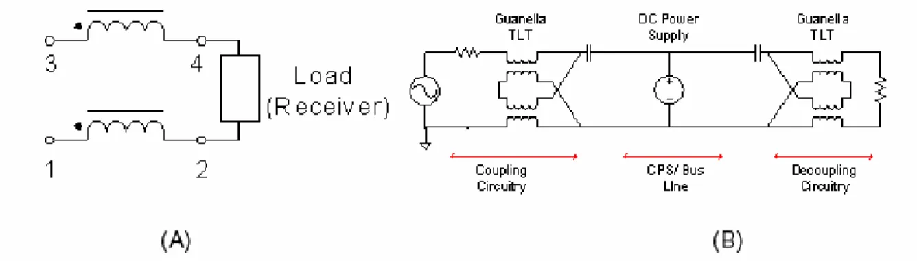
To minimize the insertion losses associated with the coupling and decoupling circuits, we propose to apply the theory of transmission line transformers, which have substantially lower insertion losses than traditional transformers for various applications [33], [34]. The basic building block of the transmission line transformer (TLT), shown in Fig. 9a, transmits energy to the load by use of transverse transmission line mode. The functionality of the circuit depends on the grounding and the connection of the terminals 1 through 4. Placing a load across terminals 2 and 4, and varying the grounded point can produce a phase inverter or delay line, for example.
Fig. 9 Basic building block for transverse transmission mode circuits and coupling and decoupling circuits with transmission line transformer
A major advantage of TLTs is that the parasitics associated with the transformer, many of which show up in parallel with the windings, are now in series with the load. Thus, even when these parasitics draw non-negligible current at high frequencies, the current is ultimately delivered to the load. As stated, a standard transformer allows this current to flow directly to ground, bypassing the load. Thus, the TLT is less susceptible to losses due to parasitics.
TLTs have not yet been used in power-line communication systems. Here, we present the design a high-fanout modem by exploiting the features of the TLT. A class of TLT configurations known as Guanella TLTs transforms apparent impedance, as seen from the CPS line. Thus, we can make the power supply input impedance, Zps, appear much higher than that of
the receivers, Zr. The system schematic, including the Guanella TLT, is shown in Fig. 9b. This
Guanella TLT performs a 1:4 impedance transformation. As will be shown later, a 1:4 transformation is adequate for our application. TLTs with a variety of parameters are available from multiple vendors. For the engineer without the time or resources to build a custom TLT, we will later outline a procedure by which the ideal TLT parameters can be found. Subsequently, the user can select an off-the-shelf TLT that best meets the requirements. However, for the purposes of modeling the system, we will first assume that we have the ability to tune our own TLT according to the methods described in [33]. Our design requirements for the tuning of these parameters will result from a careful analysis of the TLT functionality
3.2.3.
TLT Modeling
We start by analyzing the frequency characteristics of a single TLT and build a lumped parameter model competent to depict parasitic dynamics in a relevant frequency range. The TLT model we used is based on that presented by Kuo [34]. Traditional TLT models are accurate only over limited frequency ranges. Often multiple models are required to predict the operation of a TLT over a wide frequency range (up to MHz). However, Kuo’s model can predict both the low and high frequency responses of the TLT. This model incorporates the magnetizing inductance and winding resistance of the transformer in addition to the TLT windings. The difference in our formulation is due to the fact that a basic 1:1 isolating transformer is modeled in [34], whereas a 1:4 Guanella style transformer is needed. Nonetheless, the applicability of Kuo’s model to our Guanella TLT is verified by close agreement between experimental and model results. Based on this model, the ideal TLT circuit of Fig. 9b is redrawn in Fig. 10 to explicitly include the winding inductance, Lw, and winding resistance Rw.
Fig. 10 Guanella transmission line transformer model accounting for magnetizing inductance and winding resistance
Let ig,in(t) and vg,in(t) be the Guanella input current and voltage, respectively, and Zl the
equivalent load resistance placed across the output terminals. Replacing the winding inductance, Lw, with the magnetizing inductance, Lm = 2Lw, and applying impedance-based modeling
techniques, the TLT impedance Zt(s) seen at the input terminals can be written as
, , g in w l t g in l w w l m l w V (s) 8R Z s Z (s) I (s) Z 2R 2 R Z s L Z 2R ⎛ ⎞ = = ⎜ ⎟ + ⎡ ⎛ ⎞⎤ ⎝ ⎠ + ⎢ ⎥ ⎜ + ⎟ ⎢ ⎝ ⎠⎥ ⎣ ⎦ (1)
(see Appendix 10.2 for derivation)
We experimentally determine the values for Lm and Rw. Impedance data was collected with
an HP4194A impedance analyzer with bandwidth of 100MHz. The TLT was terminated with various resistors, and the impedance of the TLT-and-resistor combination was measured. The experimental values for the parasitic components were plugged into the Zt(s) function to obtain a
numerical solution. The magnetizing inductance, 5μH, and the winding resistance, 450Ω, were used along with various resistive terminations to produce Fig. 11. Note that, in Fig. 11 there is close correlation between the experimental and model performance for the TLT for load resistances of 50Ω, 100Ω, and 200Ω.
Fig. 11 Impedance of transmission line transformer with terminating resistor
3.2.4.
System Performance
Having verified the TLT model, the next step is to evaluate the entire system performance when a number of nodes are connected to the CPS line through the Guanella TLT (See Fig. 12). Note that the Guanella TLT is arranged in symmetric form for the sender and the receivers. Specifically, we are interested in broadcasting data to many receiver nodes. Gain and impedance must be evaluated as the number of nodes n becomes large. The impedance seen from the sender-side terminals is given by:
a n a V (s) Z (s) I (s) = (2)
The frequency transfer function from the input voltage of the sender to the output voltage of a receiver is given by:
d n a V (s) G (s) V (s) = (3)
Fig. 12 Circuit divided into sections: sender side components, CPS, receiver side components
Note that Va(s) is the sinusoidal voltage input generated by the sender and Vd(s) is the voltage
observed at one of the receivers at steady state. Ia(s) is the sender-side current associated with the
voltage Va(s).
To obtain (2) and (3), it is convenient to use a 2x2 matrix formulation relating input current and voltage to output current and voltage. This allows us to evaluate the system characteristics independent of the loads and on a component-by-component basis. As shown in Fig. 12 the whole system can be divided into the sender TLT, the receiver TLT, and the line characteristics including the blocking capacitor. We use (1) to write the equations of the sender side Guanella TLT in 2x2 matrix form, b a s b a V V W I I ⎡ ⎤ ⎡ ⎤⎡ ⎤ = ⎢ ⎥ ⎢ ⎥⎢ ⎥ ⎣ ⎦ ⎣ ⎦ ⎣ ⎦ (4) where s w m 1 0 2 W 1 1 2 4R 2L s ⎡ ⎤ ⎢ ⎥ = ⎢ ⎛ ⎞ ⎥ − + ⎢ ⎜ ⎟ ⎥ ⎢ ⎝ ⎠ ⎥ ⎣ ⎦ (5)
Similarly, the impedance of the receiver-side TLT can be used to write;
d c r d c V V W I I ⎡ ⎤ ⎡ ⎤⎡ ⎤ = ⎢ ⎥ ⎢ ⎥⎢ ⎥ ⎣ ⎦ ⎣ ⎦ ⎣ ⎦ (6)
where r w m 2 0 W 1 1 1 4R 2L s 2 ⎡ ⎤ ⎢ ⎥ = ⎛⎢ ⎞ ⎥ + ⎜ ⎟ ⎢⎝ ⎠ ⎥ ⎣ ⎦ (7)
Note that Ic(s) is the current flowing to each receiver at steady state. In most robotic systems,
the length of the CPS line is at most 10m. The phase shift due to the distributed impedance of the CPS conductor is not significant as long as the carrier frequency of signal transmission is lower than 10MHz. Assuming that all the blocking capacitors involved in both sender and receivers are the same and that the line impedance is dominated by the blocking capacitance, we can relate the receiver-side voltage and current to those of the sender-side as;
c b line c b V V W I I ⎡ ⎤ ⎡ ⎤⎡ ⎤ = ⎢ ⎥ ⎢ ⎥⎢ ⎥ ⎣ ⎦ ⎣ ⎦ ⎣ ⎦ (8) where line 1 1 1 1 n sC W 1 0 n ⎡ − +⎛ ⎞ ⎤ ⎜ ⎟ ⎢ ⎝ ⎠ ⎥ ⎢ ⎥ = ⎢ ⎥ ⎢ ⎥ ⎣ ⎦ (9)
Combining (4), (6), and (8) gives;
d a r line s d a V V W W W I I ⎡ ⎤ ⎡ ⎤ ⎡ ⎤ ⎡ ⎤⎡ ⎤ = ⎢ ⎥ ⎢ ⎥ ⎢ ⎥ ⎢ ⎥⎢ ⎥ ⎣ ⎦ ⎣ ⎦ ⎣ ⎦ ⎣ ⎦ ⎣ ⎦ (10)
Solving this for the impedance Va/Ia subject to the load resistance Vd = Rd/Id yields;
3 2 As Bs Cs Z (s)n 3 2 Ds Es Fs G + + = + + + (11)
where Zn(s) is the total system impedance (See Appendix 10.3 for coefficients).
As the number of nodes, n, tends to infinity, the impedance function reduces to;
1 1 lim 1 1 1 1 n 2 b s c s Z (s) Z (s)n 3 2 d s e s f s g →∞ + = = ∞ + + + (12)
These coefficients are dependent on two effective time constants, τ1 =R Cw and τ2 = L Cm . Typically, the resistance order of magnitude is hundreds of Ohms, whereas the capacitor is in 10
-9Farads, and the inductance is 10-6Henries. Thus, the time constant τ
is on the order 10-7.5s. We use these values to find b1 << c1 and d1 << e1, f1, g1. Simplifying the
coefficients, Z∞(s) can be further simplified to:
1 1 1 1 c s 2 e s f s g Z (s) + + ≅ ∞ (13)
Similarly, the gain function G(s) for n receivers is given by;
3 n 3 2 αs G (s) δs γs ςs ε = + + + (14)
(See Appendix 10.4 for coefficients)
As n approaches ∞, the gain function reduces to;
lim n n
G (s)∞ G (s) 0 →∞
= = (15)
The fact that Z∞(s) goes to a constant value and that G∞(s) goes to zero make logical sense.
As n goes to infinity (and the load resistance goes to zero), the impedance seen from the sender side will just be a function of the sender-side components. Similarly, when the load resistance goes to zero, the output voltage goes to zero, and thus, the gain goes to zero.
The plot in Fig. 13a shows the frequency dependent impedance for varying numbers of receivers, n, which has a very distinct peak. Specifically, as the number of nodes increases, the peak amplitude increases, the peak frequency decreases, and the impedance at high frequencies decreases. It should be noted that, as the number of nodes tends to infinity, the impedance peak amplitude becomes extremely high. The relevance of this fact will be addressed in the following.
The physical sense of this peaking behavior can be explained with Fig. 14. Recall the impedance form depicted in (11). Equation (11) simplifies to (13) as n approaches infinity. The peak frequency for this simplified expression is given by ωp = g1/e1. Referring the parameters of e1 and g1 from the appendix reveals that the value can be approximated by a constant
multiplied by 1/ L Cm =1/τ2. This implies the resonant behavior of a parallel L-C circuit.
Fig. 14 Simplified circuit schematic and the resulting equivalent circuit model for large n
Looking again at the circuit, we see that, as more loads are placed in parallel, the equivalent load impedance of approaches zero. This effectively changes the circuit to that of Fig. 14b. The coupling capacitor is in parallel with the winding resistance and magnetizing inductance of the TLT. The impedance function of this parallel R-L-C circuit matches the form of the impedance function Z∞(s). In the equivalent R-L-C circuit, current must always pass through the receiver
impedance as well as the coupling capacitor. Once again, the use of the TLT ensures that current will always flow into the load. Note that the typical transformer orientation of Fig. 8 allows the current to flow right back to the source without passing through the load. Thanks to the TLT, we are able to manipulate the impedance values even for large gain and large numbers of actuators n.
3.2.5.
High Fanout Design Protocol
This implies that the proposed modem design using a TLT would allow us to transmit signals to a large number of nodes simultaneously without drastically lowering the output impedance. Refer again to Fig. 13a. Even for large values of n, there remains a regime over which the impedance is high. Due to the TLT, this peak will always remain in the impedance curve. Typically, when fanout becomes large, the impedance goes to zero, and infinite current is
required to drive the system. However, in our apparatus, when fanout becomes large, there is always a frequency range for which only a nominal amount of current is required to drive the system. Of course, this frequency range is only useful if the gain of the transfer function, Gn(s),
is not too small. Therefore, we must examine the gain in the frequency range where the impedance remains high. Specifically, to use this high impedance value, we must ensure that the dip that is apparent in the gain curve of Fig. 13b is separable from the peak in the impedance curve by using the design parameters involved in the TLT modem.
Looking at the gain function, we find that the dip frequency is governed by the load resistance, Rd, and coupling capacitance, C. As mentioned, the peak is a function of the time
constant, τ1.Thus, tuning the Lm, C, and Rd parameters allows us to separate the impedance peak
and gain dip. To verify this, the authors conducted a set of experiments in which the value of magnetizing inductance was changed from 0.5μH to 5μH to 50μH. In the impedance plot, the peak value changes from 2MHz to 1.5MHz to 850kHz. However, the dip in the gain curve changes from 1.5MHz to 900kHz to 800kHz.
Thus, tuning the TLT components gives us the ability to separate the impedance peak and gain dip, and as a result, allows us to use the high-fanout design protocol. This unique contribution, based on the use of the TLT, allows us to broadcast information to multiple receivers simultaneously.
3.3. Implementation and Experiments
3.3.1.
Prototype
A proof-of-concept prototype system has been developed to demonstrate the proposed approach and verify the design and analysis methods. Fig. 15 depicts the modem used at each node of the system (a circuit diagram can be obtained from the authors directly). It consists of a transmission line transformer, a coupling capacitor, a microprocessor (PIC16F84), a signal modulation chipset, and a DC/DC converter. A DC servomotor equipped with a 12V PWM amplifier was connected to each node. The PIC is capable of performing computations for local feedback control as well as for communication with the central control unit through the CPS line.
Fig. 15 Top and bottom views of prototype modem
3.3.2.
Design
In this section a few design issues critical to the proposed method will be addressed, and experiments using the prototype will be conducted in the following section to verify the theoretical results and demonstrate the feasibility of the method. The relevant issues are the selection of the transmission frequency and the selection of modem components.
3.3.2.1.
Selection of Coupling Circuit Component Values
We design the coupling circuitry based on the analysis described in the previous section, frequency restrictions imposed by the power supply and sensors, and filtering and impedance matching conditions. The design parameters are the transmission carrier frequency f, the coupling capacitance C, and the receiver load impedance Zl. In addition, we have the TLT
impedance Zt(s), which is a function of its magnetizing inductance Lm, and parallel resistance
Rw. The design procedure is as follows.
To determine the TLT parameters Lm and Rw, we first notice that the TLT has high pass filter
characteristics. The cutoff frequency is a function of these two parameters and should be tuned such that only transmission frequencies (i.e. the mega-Hertz range as mentioned in the previous section) can pass to the CPS. Thus, the frequency f is found based on the desired transmission rate. We see, from Fig. 11, that regardless of load impedance, there is a certain frequency below which no frequency signal can pass. This can be used to select Rw and Lm. Having determined Lm
and Rw, the next step is to determine Zd(s) by evaluating the operating current and voltage for the
The first step after receiving the signal is to demodulate it. At the demodulator, the signal is divided between two ports that can sink a total of 250mA. The input voltage limit is 5V, which gives a minimum input impedance of 20Ω. This is the value used for Zc(s). Having found Zc(s),
we can next find the value for C. The receiver impedance is the TLT impedance of (1) added to the impedance of the coupling capacitance, 1/sC. For transmission line impedance matching, the impedance of the line must be matched to the impedance of the load to ensure maximum power deliver. Thus, Zt(s) is equal to the impedance of the chosen communication medium (75Ω, in our
case). Setting the impedance of the coupling capacitor and receiver equal to 75Ω, the only unknown is the capacitance value C. The parameters for our system were specified using this method and are presented in Table 1;
Table I. Coupling circuit parameter values
Parameter Value
C 3.9 nF
Lm 5.1μH
Rw 450Ω
3.3.3.
Experimental Evaluation
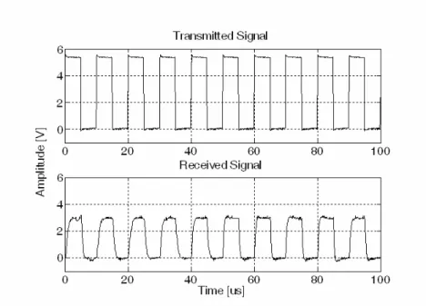
Using the coupling circuit, experiments were conducted to demonstrate the feasibility of the method. Fig. 16a shows a source digital signal before modulation and transmission, and Fig. 16b shows the demodulated signal received by one of the nodes connected to the CPS lines. Here, the pulse interval is 10μs, and the transmission rate is 100kbps. Although the high frequency noise of the power supply is visible in the received signal, the data is correctly decoded. The signal amplitude reduced only to 50% of the source amplitude. This confirms our predicted value of gain depicted in Fig. 13b. Although 30 nodes were connected, the signal gain remained high. The SNR of the received signal was 18.1.
Fig. 16 Original transmitted digital signal and received signal
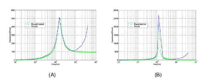
The key technical feature of the proposed method is to exploit the peak signal transmission impedance that is created through careful selection of coupling circuit parameters and the carrier frequency. It is important to note that this peak is obtainable even though we use a normal amplifier on the sender side. We verify this peak experimentally, and have presented the results for one and for thirty receivers in Fig. 17. We can evaluate (11) using the parameter values determined by the above design procedure. We can compare this result to the experimental data obtained using the impedance analyzer and the experimental apparatus. Shown in Fig. 17a is the comparison of the signal transmission impedance for a single node, n = 1. Fig. 17b is the result for the large degree-of-freedom robot with n = 30. The experimental values are shown with diamonds, and the model with the solid line. Excluding high frequencies, there is good agreement between the experiments and the model. The discrepancy at the high frequencies is due to the equivalent series resistance (ESR) of the coupling capacitor, and it is found experimentally that a coupling capacitance ESR value below 100Ω is adequate to elucidate the flat, high frequency behavior. The actual behavior is accurately predicted using our model and our design procedure.
Fig. 17 Signal transmission impedance viewed from sender for n=1, a single node, and n=30, thirty nodes
The question may arise as to how well our model predicts the limiting case as n becomes large. To address this question, it is helpful to look at the model and experimental results as a function of n. Specifically, we can look at the magnitude of the impedance peak, and the frequency at which it occurs. We showed earlier that the peak magnitude and frequency reach a maximum and minimum value (respectively) well before n reaches infinity. We now try to calculate the error in the predicted and actual steady-state values. Fig. 18a shows how the peak magnitude varies as a function of n according to the model and experimental results. There is a final error of 500Ω (20%). For the frequency plot given in Fig. 18b, there is an error of 50kHz (5%). Thus, while the limiting value of impedance magnitude shows some error, the frequency at which it occurs can be predicted quite closely. In our design procedure, this frequency is critical because it is used to help determine the parameter values of Table I. However, the magnitude is not as important. Thus, the utility of the model is verified once again in terms of its ability to predict the limiting system behavior as a function of n.