Publisher’s version / Version de l'éditeur:
Vous avez des questions? Nous pouvons vous aider. Pour communiquer directement avec un auteur, consultez la première page de la revue dans laquelle son article a été publié afin de trouver ses coordonnées. Si vous n’arrivez pas à les repérer, communiquez avec nous à PublicationsArchive-ArchivesPublications@nrc-cnrc.gc.ca.
Questions? Contact the NRC Publications Archive team at
PublicationsArchive-ArchivesPublications@nrc-cnrc.gc.ca. If you wish to email the authors directly, please see the first page of the publication for their contact information.
https://publications-cnrc.canada.ca/fra/droits
L’accès à ce site Web et l’utilisation de son contenu sont assujettis aux conditions présentées dans le site LISEZ CES CONDITIONS ATTENTIVEMENT AVANT D’UTILISER CE SITE WEB.
Journal of Physics, 59, pp. 50-53, 2007
READ THESE TERMS AND CONDITIONS CAREFULLY BEFORE USING THIS WEBSITE. https://nrc-publications.canada.ca/eng/copyright
NRC Publications Archive Record / Notice des Archives des publications du CNRC :
https://nrc-publications.canada.ca/eng/view/object/?id=43130e01-d4a3-473c-8a48-004581b0ee06 https://publications-cnrc.canada.ca/fra/voir/objet/?id=43130e01-d4a3-473c-8a48-004581b0ee06
NRC Publications Archive
Archives des publications du CNRC
This publication could be one of several versions: author’s original, accepted manuscript or the publisher’s version. / La version de cette publication peut être l’une des suivantes : la version prépublication de l’auteur, la version acceptée du manuscrit ou la version de l’éditeur.
For the publisher’s version, please access the DOI link below./ Pour consulter la version de l’éditeur, utilisez le lien DOI ci-dessous.
https://doi.org/10.1088/1742-6596/59/1/011
Access and use of this website and the material on it are subject to the Terms and Conditions set forth at
Excimer laser annealing of perovskite thin films: morphology and gas
sensing properties
Excimer laser annealing of perovskite thin films:
morphology and gas-sensor properties
X Du1, J Tunney1, M Post1 and J J Dubowski2 1
National Research Council of Canada, Ottawa, Ontario K1A 0R6, Canada
2
Université de Sherbrooke, Sherbrooke, Québec J1K 2R1, Canada
E-mail: xiaomei.du@nrc-cnrc.gc.ca
Abstract. Pulsed laser annealing was used to modify surface morphology and to enhance
crystallization of amorphous films of the p-type perovskite SrFeyCo1-yO2.5+x (y=0.5). The films
were prepared by the pulsed laser deposition technique on sapphire substrates. Both film deposition and film annealing was done using a KrF excimer laser (wavelength = 248 nm). The effects of laser energy and pulse number on film morphology, structure and gas-sensing properties were investigated. An amorphous film did not show any sensor response to oxygen composition changes, while the same film after 80 pulses of annealing at 100mJ/cm2 showed a fast response at 300˚C and 400˚C. In comparison to a dense crystalline film deposited at 700˚C, the annealed film showed a faster response to oxygen composition changes at 300oC.
1. Introduction
The family of non-stoichiometric, substitutional perovskites, SrFeyCo1-yO2.5+x, are p-type
semiconductors which have been shown to exhibit promising conductometric gas sensor properties
[1, 2]. In such sensors, changes in electrical resistance are exploited as sensor transduction signals
when the sensor materials are exposed to analyte gases. The sensing properties of thin films of these materials are strongly dependent on the film chemical structure, the microstructure and morphology. When prepared by pulsed excimer laser deposition, (PLD), the film structure depends on preparation temperature, with optimum sensor functionality being found for films grown at elevated temperatures,
T > 600oC, where high levels of crystallinity and texturing are common. Low substrate temperature deposition, particularly at ambient temperature, of these films using PLD would be attractive for applications where specific device microstructure or properties of the substrate prohibit high temperature treatment. However, films deposited by PLD at these lower temperatures are amorphous and with poor sensor functionality. It has been shown [3] that increased crystallinity enhances sensor response characteristics. Recent studies showed that pulsed laser annealing (PLA) is an attractive tool
to crystallize amorphous films
[4-8].
With this approach, the localised and rapid heating of the filmsurface and sub-surface regions facilitates fabrication of films with structural and chemical
characteristics that otherwise would require their deposition at temperatures exceeding 600 oC. A
previous study has demonstrated that laser annealing can be used to crystallize amorphous SrFeyCo1-yO2.5+x films [8]. In the present work, the effects of PLA on the morphology, structure and
gas sensing properties of amorphous thin films of SrFe0.5Co0.5O2.5+x are presented.
2. Experimental
The SrFe0.5Co0.5O2.5+x thin films were deposited by the PLD technique on
1102
sapphire using a
Lambda-Physik LPX305i excimer KrF laser operating at 248nm and with a pulse duration of about 25ns. The experimental setup has been described elsewhere [9]. The films were fabricated on sapphire substrates at ambient temperature, and for comparison purposes a film was also deposited onto a
sapphire substrate at T = 700oC. All depositions were carried out under an oxygen partial pressure of
50 © 2007 IOP Publishing Ltd
100 mTorr. The films, typically 200 nm thick, were fabricated by ablating the SrFe0.5Co0.5O2.5+x target
with the laser operating at 8 Hz and at an energy fluence of 1.5 J/cm2. The average deposition rate was
10nm/min.
Laser annealing was carried out with the same KrF excimer laser operating at 2 Hz. An area of 7 x 7
mm2 of the sample was irradiated with a flat-top beam produced by a Microlas fly-eye homogenizer.
The irradiation was carried out in an ambient atmospheric environment with up to N = 160 pulses,
each delivering a fluence selected within the range 5 to 100 mJ/cm2.
The crystallinity of the SrFe0.5Co0.5O2.5+x films before and after annealing was characterized by
X-Ray diffraction (XRD). All XRD measurements were performed on a Bruker D8 diffractometer using
Cu-KD radiation. The diffractometer was equipped for parallel beam geometry with primary and
secondary double Göbel mirrors. Data was collected using a scan step size of 2Θ = 0.02° with dwell
time of 2 sec/step. The film morphology was characterized by scanning electron microscopy (SEM) using a Philips XL 30S FEG-SEM at an acceleration voltage of 5kV.
Gas sensor functionality was determined by in-situ measurement of the electrical conductivity of the films in a custom fabricated chamber and gas flow system [1]. The conductivity measurements of the films were taken using a two-wire method in a controlled environment where the temperature could be
varied from 20oC to 500˚C and the composition of the flowing gas changed as required. The gas
mixtures used were dry air (zero grade; nominally 21%O2 in balance N2) and a 6%O2 mixture in
balance N2.
3 Results and discussion
3.1 Pulsed laser annealing
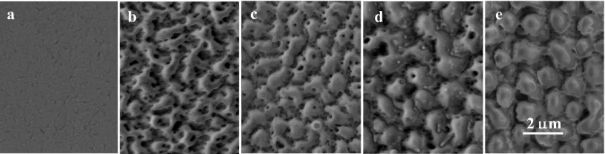
Figure 1 shows a series of SEM images obtained for the as-grown (20˚C) film and for the same film
following irradiation with 20 pulses at different fluences increasing from 40mJ/cm2to 100mJ/cm2. The
surface of the as-grown film (Figure1a) is smooth and featureless; this, together with XRD data, is in concordance with a previous TEM study suggesting that films deposited at room temperature have an amorphous structure with a domain size of ~10 nm [8]. Following 20 pulses of irradiation at
40mJ/cm2, the film morphology is observed to change substantially. Initially the irradiated film
develops a high density of pores. With an increase in fluence, the porosity decreases, and after
irradiation at100mJ/cm2 a crystallized film was produced.
c
a b d e
2Pm
Figure 1. SEM images of the as-grown film (a) and the same film following 20 pulses irradiation
at (b) 40 mJ/cm2, (c) 60 mJ/cm2, (d) 80mJ/cm2 and (e) 100mJ/cm2 at 2Hz.
2Pm
In order to optimize the experimental parameters of annealing SrFe0.5Co0.5O2.5+x films, another
series of measurements were conducted at a constant energy fluence of 100mJ/ cm2with a varying
number of pulses. Figure 2 shows a series of SEM images for the same film following irradiation with the number of pulses increasing from 5 to 160. Following only 5 pulses of laser irradiation the film morphology starts to change, and after about 40 pulses the film shows pores. The previous TEM study
showed that this treatment produces films with grain size of up to 30-40nm [8]. Generally, with an increasing number of irradiation pulses, the grain size increases and the overall film porosity decreases.
a b c d e
2Pm
Figure 2. SEM images of a SrFe0.5Co0.5O2.5+x film deposited at ambient temperature
after (a) 5, (b) 10, (c) 40, (d) 80 and (e) 160 pulses irradiation at 100mJ/cm2.
T D 30 35 40 45 50 2 (Cu-K )/deg 0 40 80 120 160 200 R e la ti v e In te n s ity
N=160
80
40
As-grown
Figure 3 shows XRD patterns obtained from samples discussed in Figure 2. It can be seen that the progress of crystallization is indicated by the
development of a diffraction peak at 24 = 32.4o,
{reflection (110) based on the cubic perovskite lattice which is the same as for 700˚C deposited films [2]} which begins to appear at around 80 pulses. However, for a higher number (N t 160) of irradiating pulses, although the crystallization is still evident with the presence of the (110) reflection, there is also a weaker XRD peak at 24
~ 28o. This is due to an unidentified phase, and is
indicative that some decomposition or phase separation has taken place.
Figure 3.
XRD spectra of a SrFe0.5Co0.5O2.5+xfilm grown at room temperature and annealed at
100mJ/cm2. N = number of laser pulses.
(110)
3.2 Sensor functionality
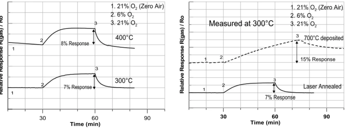
Measurement of sensor functionality by monitoring conductivity changes occurring on gas exposure
was carried out for the as-grown film and with the same film after PLA with 80 pulses at 100mJ/cm2.
Sensor response data (Figures 4 and 5) is presented in the form of Relative Response as defined by the
ratio R(gas)/R(0): where in this case R(gas) is the resistance as measured in 6% O2 and R(0) is the
“baseline” resistance as measured in zero air (21% O2). The as-grown film showed no gas sensing
response, whereas after annealing the film displayed some degree of sensitivity to changes in oxygen
composition as shown in Figure 4. Two test temperatures (300oC and 400oC) were used, and a similar
response of between 7%-8% increase in resistance was observed each time for a change in oxygen
composition of 21% to 6% in nitrogen. To compare the sensing ability at 300oC of the laser annealed
film to a higher temperature deposited film, a 700˚C deposited film was tested with the same gas compositions, and the film response is shown in Figure 5.
This data demonstrates that at the lower test temperature of 300oC, the annealed film has a more
rapid response to changing oxygen concentration than the denser film deposited at 700oC. At 300oC
the latter film clearly did not reach a stable condition of conductance over the time period of the measurement. It is proposed that the faster reaction time for the annealed film is due to the higher
potential mechanisms influencing the sensor response is gas diffusion into the film bulk, and the annealed film provides a high degree of porosity to enhance this process. Therefore the annealed film has better sensing properties than a high temperature deposited film. Hence, annealing amorphous films into a porous and, at least partially, crystallized form offers interesting advantages for the
fabrication of a SrFe0.5Co0.5O2.5+x based oxygen sensor and its integration with substrates that do not
allow the high-temperature processing.
30 60 90 Time (min) R el at ive R esp o n se R (g as) / R o 1. 21% O2 (Zero Air) 2. 6% O2 3. 21% O2 1 2 3 300°C 7% Response 8% Response 400°C 3 2 1 30 60 90 Time (min) R el at ive R e sp o n se R (g a s) / R o 1. 21% O2 (Zero Air) 2. 6% O2 3. 21% O2 Laser Annealed 1 2 3 3 Measured at 300°C 15% Response 7% Response 2 1 700°C deposited
Figure 4. Sensor response of the as-grown film
after PLA with 80 pulses at 100mJ/cm2.
Figure 5. Sensor response of the film
deposited at 700˚C and the as-grown film
after PLA.
4. Conclusions
SrFe0.5Co0.5O2.5+x thin films deposited at room temperature by PLD have an amorphous structure
which has no sensing ability to oxygen composition changes. Pulsed laser annealing (PLA) has been used to modify the morphology, structure and degree of crystallinity of these films. The gas sensing
functionality of SrFe0.5Co0.5O2.5+x thin films deposited at room temperature has been induced by
processing films at low fluence (<100mJ/cm2) using the PLA technique. The controlled evolution of
the degree of porosity of the film which is possible with PLA offers a means of optimizing sensor response characteristics. The combination of film deposition at ambient temperature by PLD, together with subsequent PLA treatment, provides a route to the integration of functional sensor films with substrates which cannot withstand high temperature processing.
5. Acknowledgements
The authors thank Q. Yang for SEM imaging and M. Kunkel for assistance with sensor response measurements.
6. References
[1] Tunney J, Post M, Du X, and Yang D 2002 J. Electrochem. Soc. 149, H113 [2] Tunney J, Whitfield P, Du X and Post M 2003 Thin Solid Films 426, 221 [3] Sanders B, Yao J and Post M 1994 Mat. Res. Soc. Proc., 343, 463.
[4] Tomita H, Nimomiya Y, Ito A and Obara M 1995 IEEE Laser and Electro.-optics Soc. Symp.
Proc 8th, 304
[5] Watakabe H, Sameshima T, Kanno H , Sadoh T and Miyao M 2004 J. Appl. Phys. 95 (11), 6457 . [6] Zhu T, Zhou Y, Liu Z 2002 Mater Sci. & Eng. B 89, 390
[7] Benatmane A, Montgomery P, Fogarassy E and Zahorski D 2003 Appl. Sur. Sci. 208-209 189 [8] Du X, Dubowski J, Post M, Wang D and Tunney J 2004 J. Vac. Sci. Technol. A 22(3) 870 [9] Sanders B and Post M 1993 Mater. Res. Soc. Symp. Proc., 285, 427