Publisher’s version / Version de l'éditeur:
Semiconductor Science and Technology, 26, 10, pp. 1-5, 2011-09-26
READ THESE TERMS AND CONDITIONS CAREFULLY BEFORE USING THIS WEBSITE.
https://nrc-publications.canada.ca/eng/copyright
Vous avez des questions? Nous pouvons vous aider. Pour communiquer directement avec un auteur, consultez la première page de la revue dans laquelle son article a été publié afin de trouver ses coordonnées. Si vous n’arrivez pas à les repérer, communiquez avec nous à [email protected].
Questions? Contact the NRC Publications Archive team at
[email protected]. If you wish to email the authors directly, please see the first page of the publication for their contact information.
NRC Publications Archive
Archives des publications du CNRC
This publication could be one of several versions: author’s original, accepted manuscript or the publisher’s version. / La version de cette publication peut être l’une des suivantes : la version prépublication de l’auteur, la version acceptée du manuscrit ou la version de l’éditeur.
For the publisher’s version, please access the DOI link below./ Pour consulter la version de l’éditeur, utilisez le lien DOI ci-dessous.
https://doi.org/10.1088/0268-1242/26/10/105021
Access and use of this website and the material on it are subject to the Terms and Conditions set forth at
On metal contacts of terahertz quantum cascade lasers with a
metal-metal waveguide
Fathololoumi, Saeed; Dupont, Emmanuel; Razavipour, S. Ghasem;
Laframboise, Sylvain R.; Parent, Guy; Wasilewski, Zbigniew; Liu, H. C.; Ban,
Dayan
https://publications-cnrc.canada.ca/fra/droits
L’accès à ce site Web et l’utilisation de son contenu sont assujettis aux conditions présentées dans le site LISEZ CES CONDITIONS ATTENTIVEMENT AVANT D’UTILISER CE SITE WEB.
NRC Publications Record / Notice d'Archives des publications de CNRC:
https://nrc-publications.canada.ca/eng/view/object/?id=e83406e7-a892-4365-a597-c791cc2d2a84 https://publications-cnrc.canada.ca/fra/voir/objet/?id=e83406e7-a892-4365-a597-c791cc2d2a84On metal contacts of terahertz quantum cascade lasers with a metal–metal waveguide
This article has been downloaded from IOPscience. Please scroll down to see the full text article. 2011 Semicond. Sci. Technol. 26 105021
(http://iopscience.iop.org/0268-1242/26/10/105021)
Download details:
IP Address: 132.246.26.120
The article was downloaded on 26/09/2011 at 17:12
Please note that terms and conditions apply.
View the table of contents for this issue, or go to the journal homepage for more
IOP PUBLISHING SEMICONDUCTORSCIENCE ANDTECHNOLOGY
Semicond. Sci. Technol. 26 (2011) 105021 (5pp) doi:10.1088/0268-1242/26/10/105021
On metal contacts of terahertz quantum
cascade lasers with a metal–metal
waveguide
Saeed Fathololoumi
1,2, Emmanuel Dupont
1, S Ghasem Razavipour
2,
Sylvain R Laframboise
1, Guy Parent
1, Zbigniew Wasilewski
1, H C Liu
1and Dayan Ban
21Institute for Microstructural Sciences, National Research Council, 1200 Montreal Rd, Ottawa, ON,
K1A0R6, Canada
2Department of Electrical and Computer Engineering, University of Waterloo, 200 University Ave W.,
Waterloo, ON, N2L3G1, Canada E-mail:[email protected]
Received 9 August 2011, in final form 26 August 2011 Published 26 September 2011
Online atstacks.iop.org/SST/26/105021
Abstract
This paper reports an experimental study of the effects of different metal claddings on the performance of terahertz quantum cascade lasers. The experimental results show that by using a metal cladding made of Ta/Cu/Au to replace that of Pd/Ge/Ti/Pt/Au, the maximum lasing temperature of the devices is increased from 132 to 172 K, and the threshold current density of the devices at 10 K can be reduced from 0.74 to 0.68 kA cm−2
. The improvement of the device performance is attributed to lower optical losses associated with the metal cladding layers. The different effects of the metal contacts on device optical properties and electrical properties are also discussed.
(Some figures in this article are in colour only in the electronic version)
1. Introduction
After nearly a decade of intense research on terahertz (THz) quantum cascade lasers (QCL), still one of the biggest challenges is to improve the maximum operating temperature (Tmax), toward room temperature operation. Many groups have
been working on designing active-region gain medium with a sufficient gain at high temperatures [1–4] and engineering low-loss waveguides [5,6]. The metal–metal (MM) waveguide structure, proposed by Williams et al [7], has a very high mode confinement factor and hence improves device performance of THz lasers with a sub-wavelength structure. Belkin
et al showed that application of copper (Cu)-based MM waveguides slightly improves Tmax, compared with gold
(Au)-based waveguides [8]. Later, Kumar et al demonstrated the record breaking Tmaxof 186 K by using Cu-based waveguides
and the resonant phonon-based active region scheme with a diagonal intersubband lasing transition [1]. However, the fabrication of Cu-based MM waveguides is very demanding, due to adhesion and oxidation problems. The stack of contact
metals in such a waveguide also results in a Schottky barrier and drops 1–2 V across the metal contacts. Such an extra voltage drop could generate up to a few watts of Joule heat when the device is in continuous-wave operation. An ohmic contact is highly desired in order to minimize the voltage drop across the laser device.
In a typical III–V semiconductor diode laser (such as GaAs or InP based) that works in the visible-light or near-infrared range, a stack of Ti/Pt/Au is usually employed to form an ohmic contact with p-type semiconductors and a stack of Ni/Ge/Au for that with n-type semiconductors [9]. Since the electron collision frequencies of most metals are in the range of 1–10 THz [10], the optical loss of contact metals in the near-infrared range becomes negligible. As the lasing frequency approaches to the THz range, the high tangent loss of the metals makes a significant contribution to the overall waveguide loss despite small penetration depth of the electromagnetic mode into the metal layers. As a result, the stack of contact metals needs to be carefully selected based on not only their electrical properties, but also their optical properties.
Semicond. Sci. Technol. 26 (2011) 105021 S Fathololoumi et al
This paper experimentally studies and compares the electrical and optical behaviors of THz QCLs with four different Au- and Cu-based metal contacts: Pd/Ge/Ti/Pt/Au, Ti/Pt/Au, Ti/Au and Ta/Cu/Au. The device with a stack of non-alloyed Ta/Cu/Au exhibits the lowest threshold current density (Jth) and the highest Tmax in pulsed mode. The
non-alloyed Ti/Au contact with a thinned Ti layer shows competitive results as also suggested in [12]. The high performance of the devices with these two non-alloyed contacts is attributed to the lower optical losses of the waveguides in spite of the formation of Schottky electrical contacts. The Ti/Pt/Au contact includes a Pt layer between Ti and Au to prevent inter-diffusion of Ti and Au atoms and hence the laser device can be annealed for metal alloying [13]. Thermal annealing the contact at 350 ◦
C for 15 s lowers the contact resistance [14]. The Pd/Ge/Ti/Pt/Au metal combination is believed to form an ohmic contact on n+GaAs [9,15] with a short diffusion of excess Ge in GaAs
[16], but its higher optical losses at THz frequencies cause the overall device performance to deteriorate.
2. Device fabrication
The THz QCLs employed in this study are based on a GaAs/Al0.15Ga0.75As three-well cascade module similar to the
one reported in [1]. The layer thicknesses are 45/ 87/ 29/ 83/ 44/ 159 ˚A—the barriers are indicated in bold fonts. The quantum well of 159 ˚A is doped with Si dopant atoms to a two-dimensional carrier concentration of 3×1010 cm−2
per module that translates into 6.7 × 1015 cm−3
doping concentration for this structure. The whole QCL structure consists of 224 repeats (10 μm thick) of this module and is grown on a semi-insulating (SI) GaAs substrate by molecular beam epitaxy. To facilitate the electrical contacts, the active region is sandwiched between 100 nm of 3 × 1018 cm−3
bottom n+ GaAs and top stack of
50 nm of 5×1018cm−3
, 10 nm of 5×1019cm−3
n+and 3.5 nm
of low-temperature (LT) grown GaAs. The last two layers are used to form a non-alloyed ohmic contact [17]. Generation of THz emission is from the optical transition between a pair of anti-crossed double well states, with a low oscillator strength of 0.35 similar to [1]. Depopulation of carriers from the lower lasing state is mediated by coupling to a wide and doped subsequent well, relaxing by longitudinal-optical (LO) phonon emission and the injection to the following module.
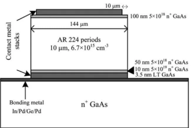
The MM waveguide of the THz QCLs was fabricated by using In–Au wafer bonding technology [18] and standard photolithography. Reactive ion etch (RIE) was performed to etch through the entire thickness of the 10 μm thick active region, which minimizes the lateral spreading of current flow. Other details of the device fabrication can be found in [19]. Figure1shows the schematic cross-section of fabricated QCL devices with a MM waveguide. Using scanning electron microscopy, the area of the tested laser facets was measured; the average width of the ridge waveguides varies between 141 and 147 μm and the top metal width is 120 μm. The variations in the ridge size and shape can be accounted to the reproducibility of the RIE that is not fully controlled. The substrate of the samples was thinned down to ∼150 μm to
Figure 1.Schematic diagram of the cross section of fabricated THz QCLs with a metal–metal waveguide. The active region (AR) is based on a three-well cascade module that is repeated 224 times. The thickness of the active region is ∼10 μm. The top
semiconductor contact layer is 100 nm thick n+GaAs doped at
3 × 1018cm−3. The bottom semiconductor contact layers consist of
50 nm thick n+GaAs doped at 5 × 1018cm−3, 10 nm thick n+GaAs
doped at 5 × 1019cm−3and 3.5 nm of LT GaAs. The semiconductor
active region is sandwiched by two metal claddings from the top and the bottom.
facilitate heat dissipation from the active region to a heat sink underneath [19]. The sample was cleaved into laser bars with an ∼1 mm long Fabry–Perot resonator. The laser bars were indium soldered (epi-layer side up) on oxygen-free copper packages and then mounted in a Janis closed-cycle cryostat for measurements.
Four groups (A–D) of QCL devices with different metal stacks for the electrical contacts were fabricated and tested to examine their effects on device performance. The metal stack employed in group A is Pd/Ge/Ti/Pt/Au (55/100/25/55/ 300 nm), which was annealed at 380◦
C for 15 s and formed an ohmic contact with the n-type GaAs contact layer. The metal stack employed in group B is Ti/Pt/Au (25/55/300 nm), annealed at 350◦
C for 15 s. The annealing of the first two groups yielded alloyed contacts. The metal stack employed in group C is the simplest, consisting only two layers Ti/Au (5/300 nm, non-annealed). The metal stack employed in group D is Ta/Cu/Au (10/500/100 nm, non-annealed). As we will show later, the optical loss of the last two metal stacks is relatively low and Cu is believed to be one of the least lossy metals in the THz frequency range. To ensure the comparison of the results, four small wafer pieces (1 cm by 1 cm) were cut from the same wafer and processed under the exactly same conditions.
3. Results and discussions
In THz QCLs with MM waveguides, the waveguide losses can vary to a large extent depending on the different constituent metals in the metal claddings. Figure2compares the calculated temperature-dependent waveguide losses for the structure with the metal claddings made of the four aforementioned metal stacks. The waveguide losses were calculated from simulating the complete 2D structure of the device shown schematically in figure 1, at a lasing
Semicond. Sci. Technol. 26 (2011) 105021 S Fathololoumi et al
Figure 2.Calculated waveguide losses of THz QCLs with different metal claddings. The curves from the top to the bottom correspond to metal claddings made of Pd/Ge/Ti/Pt/Au, Ti/Pt/Au, Ti/Au and Ta/Cu/Au. The waveguide losses increase with temperature for all cases. The device with a metal cladding made of Ta/Cu/Au has the lowest waveguide loss. The right vertical axis shows the simulated optical gain based on a simplified density matrix model [4], which includes intersubband LO-phonon, ionized impurity and interface roughness scatterings. At Tmax(136, 146, 170, 172 K) the
disagreement between the simulated waveguide loss and optical gain is represented by the vertical double arrows. This disagreement is too high to be solely accounted by the mirror loss. This could be explained by the inaccuracy of the models used for optical gain and waveguide loss, as well as waveguide imperfections.
frequency of 3.75 THz. It consists of 10 μm thick and 144 μm wide MM THz QCL waveguides. The temperature-dependent permittivity and mobility of the active and n+
regions were calculated using the data in [20,21], respectively. The optical constants for the metals (plasma and carrier collision frequencies) were taken from [10] and the complex permittivity of various layers was calculated using the Drude– Lorentz approximation as [10] ǫ(ω) = ǫ∞− ω2p ω2+ j ωω 0 , (1)
where ǫ∞ is the high-frequency limit of the material
permittivity, and ωp and ω0 are the plasma and electron
collision frequencies, respectively. For the sake of simplicity, the waveguide loss values are estimated using an isotropic Drude model for the laser active region, whereas a more rigorous approach would include (i) the Drude model only in the quantum-well plane [11] and (ii) use of an intersubband absorption model in the growth direction [22]. The tempera-ture dependence of metal permittivity is extracted from the conductivity temperature dependence data in [23]. The full details of the waveguide structure, including the thin highly doped GaAs layers below and above the 10 μm thick active region and the thin metal layers of platinum, gold and copper in the metal stacks, were taken into account in the simulation. Due to lack of information about the metal layers (titanium, palladium germanium and tantalum), these layers are modeled by using the temperature-independent parameters of tungsten. The calculated waveguide losses in figure 2 are in good agreement with the experimental results reported by other groups [24,25]. The simulation of the optical gain, on the other hand, was performed using the simplified density matrix model
presented in [4]. The gain model includes intersubband LO-phonon, ionized impurity and interface roughness scattering mechanisms. Some key simulation parameters deployed in our simulations are electron heating temperature (90 K), pure dephasing time constant (0.36 ps) and lasing dephasing time constant (1.15 ps). Other simulation parameters can be found in [4].
As shown in figure 2, the metal cladding of Pd/Ge/Ti/Pt/Au exhibits the highest waveguide loss (αW)
over the temperature range of the simulation. The metal cladding of Ti/Pt/Au shows the second-highest waveguide loss, with a small reduction of ∼3–5 cm−1
in αWcompared to
that of Pd/Ge/Ti/Pt/Au over the temperature range from 90 to 250 K. The metal cladding of Ti/Au shows a further reduction of > 10 cm−1
in waveguide loss. The metal cladding of Ta/Cu/Au has the lowest waveguide loss, ∼18 cm−1
even at 160 K. The effects of the mirror losses of the different metal contacts are not taken into account in the following discussion. This is because that the mirror loss is much smaller compared to the waveguide loss in MM THz QCLs [5], and the variation of the mirror loss due to different metal contacts is therefore negligible. Since the Jth and the Tmaxof the THz QCLs are
strongly affected by the waveguide losses, it is expected that the performance of the devices with different metal claddings could be significantly different.
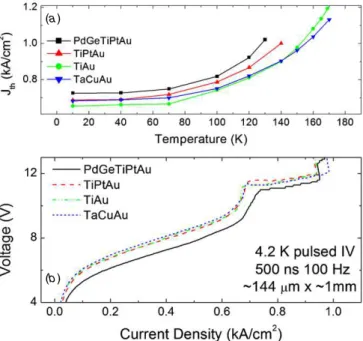
Figure3 shows the light–current (LI) characteristics of the THz QCLs (A–D) at temperatures from 10 to 170 K. The devices were biased in pulsed mode with a pulse duration of 250 ns and repetition rate of 1 kHz. The pulse duty cycle is so small (only 2.5 × 10⁻⁴
) that the average device electrical power consumption is in the milli-watt range and thus the Joule heating in the device is negligible. At T = 10 K, the Jth values are 0.74 kA cm−2 for device
A (with Pd/Ge/Ti/Pt/Au metal claddings), 0.69 kA cm−2
for device B (with Ti/Pt/Au metal claddings), 0.66 kA cm−2
for device C (with Ti/Au metal claddings) and
0.68 kA cm−2
for device D (with Ta/Cu/Au metal claddings). Device A clearly shows a higher Jthvalue, which is correlated
to the highest value of the calculated waveguide losses of the four different structures.
Maximum lasing temperature is an important performance indicator of THz QCL devices. Tmax is determined when
the temperature-degrading optical gain reaches the optical waveguide loss (figure 2). Devices with lower loss are hence expected to show higher lasing temperatures. The experimental results show Tmax of 136 K for device A,
146 K for device B, 170 K for device C and 172 K for device D. The improvement in temperature performance from devices A to D could mainly be attributed to the reduction of waveguide losses, due to the different metal contacts [8]. Device D has the lowest waveguide loss so it attains the highest Tmax.
The selection of different metal contacts also affects the electrical behaviors of the THz QCLs. Figure 4(a) shows the measured Jth of the four devices (A–D) as a function of
temperature from 10 K to their respective Tmax. Within the
experimental uncertainty, one can find a fairly good correlation between the threshold current density and the calculated waveguide loss—the device with a lower waveguide loss
Semicond. Sci. Technol. 26 (2011) 105021 S Fathololoumi et al
(a)
(b)
(c)
(d )
Figure 3.Temperature-dependent LI curves for the THz QCL devices (A–D) with different metal claddings. The ridge
waveguides of all devices are 150 μm wide and 1 mm long and are fabricated using (a) Pd/Ge/Ti/Pt/Au, (b) Ti/Pt/Au, (c) Ti/Au and (d) Ta/Cu/Au metal contacts. The bias is applied in pulsed mode (pulse width = 250 ns, repetition rate = 1 kHz). The Ta/Cu/Au shows the highest Tmaxand lowest Jthat 10 K.
exhibits a lower Jth, particularly at higher temperatures. The
tested devices were lasing at longer lasing wavelengths than the designed value at lower temperatures, while the calculated waveguide losses and optical gain were obtained at the designed lasing wavelength. This could lead to discrepancies between the simulation and experimental results, as shown in figure 2. Device A exhibits the highest Jth over the entire
temperature range, which stems from the highest waveguide loss as shown in figure2. The Jth of device D, which has
the lowest loss, is slightly higher than that of device C at low temperatures. This might be attributed to the different profile of the ridge sidewalls. Indeed, SEM inspection indicates that the sidewalls of device D are much more vertical than the others, which widens the gap between the top metal and the edge of the ridge (∼12 μm for devices D versus ∼10 μm for the others). The optical image also shows that device D was cleaved into the shortest Fabry–Perot ridge waveguide (930 μm), and hence its mirror loss should be the highest among the four devices. The higher mirror loss would give rise to a higher threshold current density. Figure4(b) shows the measured current–voltage (IV) curves of the four devices (A–D). As mentioned earlier, Pd/Ge/Ti/Pt/Au forms an ohmic contact with the n+GaAs layer; device A therefore exhibits the
lowest bias voltage under any given electrical current among
(a)
(b)
Figure 4.(a) The threshold current densities of the devices (A–D) as a function of temperature. (b) Current–voltage (IV) curves of the devices at 10 K. Device A exhibits the best IV characteristics due to its ohmic metal contacts. Devices B–D show inferior IV
characteristics in which extra bias (∼ 0.8V) is needed to overcome the Schottky barrier at the metal/semiconductor interface.
the four devices. Other metal stacks form more or less a similar Schottky contact with the n+ GaAs layer, so extra
bias voltage (∼ 0.8 V) needs to be applied to overcome the Schottky barrier between the top metals and the semiconductor layer (non-alloyed bottom contact with LT-GaAs should form an ohmic contact). For a given bias of 10 V (below lasing threshold) the current density was measured to be 0.7 kA cm−2
for device A, 0.66 kA cm−2
for devices B and C and 0.65 kA cm−2
for device D. The IV curves in figure 4(b) indicate that the electrical current is injected into device A most easily, while other devices show similar extra resistance. The extra voltage drop to overcome the Schottky energetic barrier at the metal/semiconductor interface in devices B, C and D leads to extra electrical power consumption, which eventually converts to Joule heat. The active region of the device could be over-heated if the Joule heat cannot be dissipated away quickly and gets accumulated in the core. This can be the case when the device is operated in continuous-wave mode (i.e. under dc bias). The device performance deterioration due to Joule heating may become substantial and completely offsets the benefits arising from the lower waveguide losses in non-ohmic metal claddings. Nevertheless, when the devices are biased in pulsed mode with a low duty cycle (such as in the measurements of this study), the improvement in temperature performance due to lower waveguide losses overwhelms the deterioration in electrical current injection. This explains why device D exhibits the best performance.
4. Conclusion
Four groups of THz QCLs with different metal contacts were fabricated and characterized. The stack of annealed
Semicond. Sci. Technol. 26 (2011) 105021 S Fathololoumi et al
Pd/Ge/Ti/Pt/Au can form an ohmic contact with an n-GaAs semiconductor layer; however, the metal contact has a high optical loss, which degrades the device performance. On the other hand, other metal stacks, annealed Ti/Pt/Au, non-annealed Ti/Au and non-non-annealed Ta/Cu/Au, form a Schottky-like junction with the n+ GaAs layer but exhibit lower
waveguide losses. Among them, Ta/Cu/Au has the lowest calculated waveguide losses at 3.75 THz. Consequently, the device with such metal stack claddings exhibits the highest Tmax in pulsed mode. The metal stack of Ti/Au with a
thinned Ti layer (only 5 nm thick) also shows relatively low waveguide losses (very close to that of Ta/Cu/Au), and exhibits comparable Tmax and threshold current density to
that of Ta/Cu/Au. It is worth pointing out that it is much less demanding to fabricate the Ti/Au-based metal claddings than the Cu-based ones. The experimental results reveal that lowering the optical losses of the metal claddings in THz QCLs becomes more prominently important for enhancing Tmaxand
reducing Jthin pulsed mode operation.
Acknowledgments
The authors would like to acknowledge support from Natural Science and Engineering Research Council (NSERC) of Canada, from the University of Waterloo, from Canadian Foundation of Innovation (CFI) and from the Ministry of Research and Innovation of Ontario.
References
[1] Kumar S, Hu Q and Reno J L 2009 186 K operation of terahertz quantum-cascade lasers based on a diagonal design Appl. Phys Lett.94131105
[2] Kumar S, Chan C W I, Hu Q and Reno J L 2009 Two-well terahertz quantum-cascade laser with direct
intrawell-phonon depopulation Appl. Phys Lett.95141110
[3] Scalari G, Amanti M I, Walther C, Terazzi R, Beck M and Faist J 2010 Broadband THz lasing from a photon-phonon quantum cascade structure Opt. Express188043–8052
[4] Dupont E, Fathololoumi S and Liu H C 2010 Simplified density-matrix model applied to three-well terahertz quantum cascade lasers Phys. Rev. B81205311
[5] Kohen S, Williams B S and Hu Q 2005 Electromagnetic modeling of terahertz quantum cascade laser waveguides and resonators J. Appl. Phys.97053106
[6] Tavallaee A A, Hon P C, Mehta K, Itoh T and Williams B S 2010 Zero-index terahertz quantum-cascade metamaterial lasers IEEE J. Quantum Electron.461091–8
[7] Williams B S, Kumar S, Callebaut H and Hu Q 2003 Terahertz quantum-cascade laser at λ ∼ 100 μm using metal
waveguide for mode confinement Appl. Phys Lett.832124–6
[8] Belkin M A, Fan J A, Hormoz S, Capasso F, Khanna S P, Lachab M, Davies A G and Linfield E H 2008 Terahertz
quantum cascade lasers with copper metal–metal
waveguides operating up to 178 K Opt. Express163242–8
[9] Baca A G, Ren F, Zolper J C, Briggs R D and Pearton S J 1997 A survey of ohmic contacts to III–V compound
semiconductors Thin Solid Films308–309599–606
[10] Ordal M A, Bell R J, Alexander R W, Long L L and Querry M R 1985 Optical properties of fourteen metals in the infrared and far-infrared: Al, Co, Cu, Au, Pb, Mo, Ni, Pd, Pt, Ag, Ti, V, and W Appl. Opt.244493–9
[11] Bogdanov A A and Suris R A 2011 Mode structure of a quantum cascade laser Phys. Rev. B83125316
[12] Walther C, Scalari G, Faist J, Beere H and Ritchie D 2006 Low frequency terahertz quantum cascade laser operating from 1.6 to 1.8 THz Appl. Phys Lett.89231121
[13] Masahiro K and Noboru S 1993 Effects of temperature, thickness and atmosphere on mixing in Au–Ti bilayer thin films J. Mater. Sci.285088–91
[14] Sehgal B K, Bhattacharya B, Vinayak S and Gulati R 1998 Thermal reliability of n-GaAs/Ti/Pt/Au Schottky contacts with thin Ti films for reduced gate resistance Thin Solid
Films330146–9
[15] Lim J, Mun J, An S, Nam S, Kwak M, Kim H and Lee J 2000 PdGe-based ohmic contact on n-gaAs with highly and poorly doped layers Japan. J. Appl. Phys.392546–9
[16] Ivey D G, Eicher S, Wingar S and Lester T 1997 Performance of PdGe-based ohmic contacts to n-type GaAs J. Mater.
Sci.: Mater. Electron.6363–8
[17] Patkar M P, Chin T P, Woodall J M, Lundstrom M S and Mellocha M R 1995 Very low resistance nonalloyed ohmic contacts using low-temperature molecular beam epitaxy of GaAs Appl. Phys. Lett.661412–4
[18] Ban D, Wchter M, Liu H C, Wasilewski Z R, Buchanan M and Aers G C 2006 Terahertz quantum cascade lasers by wafer fusion: fabrication, characterization and doping effect
J. Vac. Sci. Technol.A24778–82
[19] Fathololoumi S, Ban D, Luo H, Dupont E, Laframboise S R, Boucherif A and Liu H C 2008 Thermal behavior investigation of terahertz quantum-cascade lasers IEEE J.
Quantum Electron.441139–44
[20] Blakemore J S 1982 Semiconducting and other major properties of gallium arsenide J. Appl. Phys.53R123–81
[21] Chin V W L, Osotchan T, Vaughan M R, Tansley T L, Griffiyhs G J and Kachwalla Z 1993 Hall and drift mobilities in molecular beam epitaxial grown GaAs
J. Electron. Mater.221317–21
[22] Ajili L, Scalari G, Giovannini M, Hoyler N and Faist J 2006 Doping in quantum cascade lasers: II. GaAs/Al0.15Ga0.85As
terahertz devices J. Appl. Phys.100043102
[23] Lide D R 2008 Electrical resistivity of pure metals CRC
Handbook of Chemistry and Physics88th edn (Internet Version 2008) (Boca Raton, FL: CRC Press/Taylor and Francis)
[24] Kroll J, Darmo J, Dhillon S S, Marcadet X, Calligaro M, Sirtori C and Unterrainer K 2007 Phase-resolved measurements of stimulated emission in a laser Nature
449698–702
[25] Burghoff D, Kao T Y, Ban D, Lee A W M, Hu Q and Reno J 2011 A terahertz pulse emitter monolithically integrated with a quantum cascade laser Appl. Phys. Lett.98061112