HAL Id: cel-00843641
https://cel.archives-ouvertes.fr/cel-00843641v7
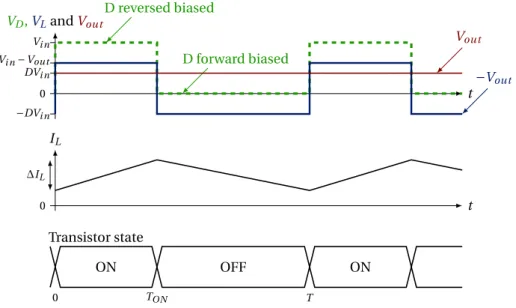
Submitted on 10 May 2019 (v7), last revised 26 May 2021 (v8)
HAL is a multi-disciplinary open access
archive for the deposit and dissemination of
sci-entific research documents, whether they are
pub-lished or not. The documents may come from
teaching and research institutions in France or
abroad, or from public or private research centers.
L’archive ouverte pluridisciplinaire HAL, est
destinée au dépôt et à la diffusion de documents
scientifiques de niveau recherche, publiés ou non,
émanant des établissements d’enseignement et de
recherche français ou étrangers, des laboratoires
publics ou privés.
Advanced Electronic Systems
Damien Prêle
To cite this version:
Damien Prêle. Advanced Electronic Systems. Master. Advanced Electronic Systems, Hanoi, Vietnam.
2019, pp.153. �cel-00843641v7�
Advanced Electronic Systems
ST 11.7 - Master 1 SPACE
University of Science and Technology of Hanoi
Université de Paris
Lectures, tutorials and labs
2018-2019
Damien PRÊLE
Contents
I Filters
7
1 Filters 9
1.1 Introduction . . . 9
1.2 Filter parameters . . . 9
1.2.1 Voltage transfer function . . . 9
1.2.2 S plane (Laplace domain) . . . 11
1.2.3 Bode plot (Fourier domain) . . . 13
1.3 Cascading filter stages . . . 16
1.3.1 Polynomial equations . . . 17
1.3.2 Filter Tables . . . 20
1.3.3 The use of filter tables . . . 22
1.3.4 Conversion from low-pass filter . . . 23
1.4 Filter synthesis . . . 25
1.4.1 Sallen-Key topology . . . 25
1.5 Amplitude responses . . . 28
1.5.1 Filter specifications . . . 28
1.5.2 Amplitude response curves . . . 29
1.6 Switched capacitor filters . . . 33
1.6.1 Switched capacitor . . . 33
1.6.2 Switched capacitor filters . . . 34
Tutorial 37 1.7 First order passive filter . . . 37
1.8 Second order passive filter . . . 38
1.9 Active filter - Sallen-Key topology . . . 38
1.10 5t horder Butterworth low-pass filter fc= 100 Hz . . . 39
1.11 4t horder Chebyshev (3dB) low-pass filter fc= 1 kHz . . . 39
1.12 6t horder Bessel high-passfilter . . . 39
1.13 Filter synthesis from template . . . 39
1.13.1 Low pass-filter synthesis . . . 39
1.13.2 Removing harmonics frequencies . . . 40
Lab 41 1.14 Passive filter . . . 41
1.15 Low pass-filter synthesis . . . 42
1.16 Removing harmonics frequencies . . . 43
II DCDC Converters
45
2 DC/DC converters 47 2.1 Introduction . . . 47 2.1.1 Advantages/Disadvantages . . . 47 2.1.2 Applications . . . 48 2.2 DC/DC converters . . . 48 2.2.1 Buck converters . . . . 49 2.2.2 Boost converters . . . . 502.2.3 Buck-boost inverting converters . . . . 52
2.2.4 Flyback converters . . . . 53
2.3 Control . . . 54
2.3.1 Feedback regulation . . . 54
2.3.2 Voltage regulation . . . 54
Tutorial 56 2.4 DC/DC converter and duty cycle . . . 57
2.5 Triangle wave oscillator for PWM . . . 57
2.6 Preparation of the practical work . . . 58
2.6.1 Triangle wave oscillator under a single VCCpower supply . . . 58
2.6.2 Comparator . . . 59
2.6.3 Switching transistor . . . 59
2.6.4 DC/DC buck converter . . . . 60
2.6.5 Voltage regulation . . . 60
Lab 63 2.7 Pulse Width Modulation (PWM) . . . 63
2.8 Transistor driver . . . 64
2.9 Waveform signals in a buck converter . . . . 64
2.10 Voltage regulation . . . 65
III Phase Locked Loop
67
3 Phase Locked Loop 69 3.1 Introduction . . . 693.2 Description . . . 69
3.2.1 Phase detector/comparator . . . 70
3.2.2 Voltage Control Oscillator - VCO . . . 73
3.3 Frequency range . . . 74
3.3.1 Lock range 2∆fL. . . 74
3.3.2 Capture range 2∆fC . . . 75
3.4 Frequency response . . . 76
3.4.1 One pole loop filter . . . 77
3.4.2 One pole - one zero loop filter (like PID) . . . 77
Tutorial 79 3.5 Frequency Shift Keying (FSK) demodulation . . . 79
3.5.1 VCO setting . . . 80
3.5.2 Loop filter and PLL response . . . 80
3.6 PLL as a frequency multiplier . . . 81
3.6.1 PLL with one pole - one zero loop filter . . . 81
3.6.2 Loop with multiplication . . . 82
Lab 84
3.7 Frequency Shift Keying (FSK) demodulation . . . 85
3.7.1 FSK demodulation using a CD4046 PLL . . . 85
3.7.2 Frequency Shift Keying (FSK) signal using the function generator . . . 86
3.8 Frequency multiplier . . . 87
3.8.1 PLL with one pole - one zero loop filter . . . 87
3.8.2 Loop with multiplication . . . 87
3.8.3 Frequency synthesizes . . . 88
IV Modulation
89
4 Modulation 91 4.1 Introduction . . . 91 4.2 Amplitude modulation . . . 92 4.2.1 Modulation index . . . 94 4.3 Amplitude demodulation . . . 95 4.3.1 Envelope demodulation . . . 95 4.3.2 Product demodulation . . . 97 Tutorial 103 4.4 Double Side Bande Amplitude Modulation . . . 1034.4.1 Modulation without carrier transmission . . . 103
4.4.2 The use of an AD633 as multiplier . . . 104
4.4.3 Product detection . . . 104
4.4.4 Modulation with carrier transmission using an AD633 . . . 104
4.4.5 Modulation index adjustment . . . 105
4.4.6 Enveloppe detection . . . 105
Lab 107 4.5 Amplitude modulation as a simple multiplication . . . 107
4.5.1 Modulation . . . 107
4.5.2 Product detection . . . 108
4.5.3 Modulation with adding carrier . . . 108
4.5.4 Envelope detection . . . 109
A Polynomials filter tables 111
B Frequency response of polynomial filters 113 C Angles, sin and cos transformation formulas 119
D TL081 Data Sheet 121
E LM311 Data Sheet 123
F Zener diodes Data Sheet 125
G BDX54 Data Sheet 127
H Rectifier Data Sheet 129
I LM158 Data Sheet 131
J CD4046 Data Sheet 133
K CD4018 Data Sheet 139
M Signal diode Data Sheet 147 N 78XX Linear voltage regulator Data Sheet 149
Foreword
T
HEpresent document is based on four lectures given for Master of Space and Aeronautics in Univer-sity of Science and Technology of Hanoi. It consists of four parts. The first one is devoted to filters, while the second one deals with DC/DC converter, the third one discusses the phase locked loop and the last the modulation. For convenience of the readers the work is organized so that each part is self-contained and can be read independently. These four electronic systems are chosen because they are representative of critical elements encountered in spacecraft; wether for power supply or for data trans-mission.Acknowledgements : Damien Prêle was teaching assistants in Paris-6 University for 4 years with professor Michel REDON.
Topics of this lecture are inspired from M. Redon’s lectures given at Paris-6 University for electronic masters. Therefore, this lecture is dedicated to the memory of professor Michel REDON who gave to the author his understanding of the electronic and helped him to start teaching it.
Moreover, the author would like to express his gratitude to Miss Nguyen Phuong Mai and Mr. Pham Ngoc Dong for their help for the preparation of this teaching in the University of Science and Technology of Hanoi.
Part I
Filters
1
Filters
1.1 Introduction
A
filter performs a frequency-dependent signal processing. A filter is generally used to select a useful frequency band out from a wide band signal (example : to isolate station in radio receiver). It is also used to remove unwanted parasitic frequency band (example : rejection of the 50-60 Hz line frequency or DC blocking). Analogue to digital converter also require anti-aliasing low-pass filters.The most common filters are low-pass, high-pass, band-pass and band-stop (or notch if the rejection band is narrow) filters :
f Low-pass f High-pass f Band-pass f Band-stop
Figure 1.1: Transfer function of ideal filter : Fixed gain in the pass band and zero gain everywhere else ; transition at the cutoff frequency.
To do an electronic filter, devices which have frequency-dependent electric parameter as L and
C impedances are required. The use of these reactive impedances*into a voltage bridge is the most
common method to do a filtering ; this is called passive filtering. Passive (R,L,C) filter is used at high
frequencies due to the low L and C values required. But, at frequency lower than 1 MHz, it is more common to use active filters made by an operational amplifier in addition to R and C with reasonable
values. Furthermore, active filter parameters are less affected†by load impedances than passive one.
1.2 Filter parameters
1.2.1 Voltage transfer function
Passive low-pass filter example : a first order low-pass filter is made by R-C or L-R circuit as a voltage
divider with frequency-dependent impedance. Capacitor impedance (ZC=jC1ω) decreases at high
fre-quency‡while inductor impedance (ZL= j Lω) increases. Capacitor is then put across output voltage
*A reactive impedance is a purely imaginary impedance.
†Active filter allows to separate the filter parameters with those matching impedance. ‡angular frequencyω = 2πf
1.2. FILTER PARAMETERS 1. FILTERS
and inductor between input and output voltage (Fig. 1.2) to perform low pass filtering.
vi n R ii n C "iout" vout vi n L R vout vi n L C vout
Figure 1.2: Passive low-pass filter : first order R-C, first order L-R and second order L-C.
Generalization : whatever impedances Zx of the voltage bridge shown in figure 1.3, voltage transfer
functions H are generalized as expression 1.1 by calculating the divider’s voltage ratio using Kirchhoff’s voltage law*.
vi n Z1
Z2
vout=Z1Z+Z2 2vi n
Figure 1.3: Impedance bridge voltage divider.
H (ω) =vout vi n =
Z2 Z1+ Z2
(1.1) Voltage transfer functions of filters given in figure 1.2 are then expressed as :
HRC= ZC R + ZC = 1 jCω R +jC1ω =⇒ HRC= 1 1 + j RC ω (1.2) cut-off frequency ≡ |HRC| = 1 p 2 → RC ωc= 1 → fc ¯ ¯ ¯ RC = 1 2πRC HLR= R R + ZL = R R + j Lω =⇒ HLR= 1 1 + jLRω (1.3) fc ¯ ¯ ¯ LR= R 2πL HLC= ZC ZL+ ZC = 1 jCω j Lω +jC1ω =⇒ HLC= 1 1 − LC ω2 (1.4) f0 ¯ ¯ ¯ LC= 1 2πpLC
+A filter can also be used to convert a current to a voltage or a voltage to a current in addition to a simple filtering†. Considering for example the first R-C low-pass filter in figure 1.2. We can define *The sum of the voltage sources in a closed loop is equivalent to the sum of the potential drops in that loop : vi n= Z1×
vout
Z2
| {z }
ii n="iout" + vout
†To filter a current, two impedances in parallel are require : current divider. In our example without load impedance i i n= iout.
Current transfer function"iout"
1. FILTERS 1.2. FILTER PARAMETERS
trans-impedance transfer functionvout
ii n and also the trans-admittance transfer function "iout" vi n : vout ii n = vout "iout"= ZC= 1 jCω −→ Integrator (1.5) "iout" vi n = 1 R + ZC = 1 R +jC1ω = jCω 1 + j RC ω −→ High-pass filter (1.6)
1.2.2 S plane (Laplace domain)
For transient analysis, filter transfer function H must be represented as a function of the complex num-ber s :
s = σ + j ω (1.7)
Then, reactive impedances are expressed as function of this complex number :
ZL= Ls (1.8)
ZC=
1
C s (1.9)
Frequency response and stability information can be revealed by plotting in a complex plane (s plane) roots values of H (s) numerator (zero) and denominator (pole).
• Poles are values of s such that transfer function |H| → ∞, • Zeros are values of s such that transfer function |H| = 0.
Considering the band-pass filter of the figure 1.4, the transfer function HLC R=vvouti n is given by
equa-tion 1.10.
vi n
L
C R
vout
Figure 1.4: Passive band-pass LCR filter.
HLC R(s) = R R + Ls +C s1 =
RC s
1 + RC s + LC s2 (1.10)
The order of the filter (Fig. 1.4) is given by the degree of the denominator of the expression 1.10. A
zero corresponds the numerator equal to zero. A pole is given by the denominator equal to zero. Each
pole provides a -20dB/decade slope of the transfer function ; each zero a + 20 dB/decade*. Zero and
pole can be real or complex. When they are complex, they have a conjugate pair†.
Expression 1.10 is characterized by a zero at s = 0 and two conjugate poles obtained by nulling it’s denominator (eq. 1.11)‡. 0 = 1 + RC s + LC s2−−−−−→ d i scr i . ∆ = (RC) 2 − 4LC −−−−→ r oot s sp= −RC ±p(RC )2− 4LC 2LC (1.11)
*H [d B ] = 20log H[l i n.] and a decade correspond to a variation by a factor of 10 in frequency. A times 10 ordinate increasing
on a decade (times 10 abscissa increasing) correspond to a 20dB/decade slope on a logarithmic scale or also 6dB/octave. A -20dB/decade then correspond to a transfer function decreasing by a factor of 10 on a decade
†each conjugate pair has the same real part, but imaginary parts equal in magnitude and opposite in sign ‡The roots (zeros) of a polynomial of degree 2 (quadratic function) ax2+ bx + c = 0 are x =−b±p∆
2a where the discriminant is
∆ = b2
− 4ac
1.2. FILTER PARAMETERS 1. FILTERS
The discriminant∆ could be positive, null or negative as shown in figure 1.5. The boundary (∆ = 0) between negative and positive discriminant is given by the equation (RC )2= 4LC and could be rewrite
1 2=
p
L/C
R Qwhich is the expression of a parameter called the quality factor Q.
Figure 1.5: Discriminant∆ = (RC)2− 4LC value as function of (RC )2and 4LC . For a given C, ifRLis large → spis real, if LRis large → spis imaginary.
Nature (real or imaginary) of the roots is reported in the table 1.1. ∆ = (RC)2− 4LC roots s p Q = p L/C R > 0 2 real < 1/2 = 0 1 real double = 1/2 < 0 2 complex conjugates > 1/2
Table 1.1: Link between discriminant sign and nature of the roots. Conditions on the R, L and C device values are reported expressed as the quality factor Q.
Roots are expressed as two complex conjugate roots*: the poles sp
1and sp2given on 1.12. sp1,2= −R 2L ± j s 1 LC − µR 2L ¶2 (1.12)
The natural angular frequencyω0is the module of the pole :
ω0= |sp1,2| =
1 p
LC (1.13)
In a s plane, pole and zero allow to locate where the magnitude of the transfer function is large (near pole), and where it is small (near zero). This provides us understanding of what the filter does at different frequencies and is used to study the stability. Figure 1.6 shows pole (6) and zero (l) in a s plane.
A causal linear system is stable if real part of all poles is negative. On the s plane, this corresponds to a pole localization at the left side (Fig. 1.7).
+Laplace notation s = σ + j ω is required to study stability condition and transient (time domain) analysis. However, for steady state signal (frequency domain) analysis, Fourier notation s = j ω is preferred to do harmonic analysis.
1. FILTERS 1.2. FILTER PARAMETERS σ jω 1 p LC −2LR l 6 q 1 LC − ¡R 2L ¢2 6 − q 1 LC − ¡R 2L ¢2
Figure 1.6: Pole (6) and zero (l) representation of the RLC filter (Fig. 1.4) into the s plane.
σ jω 6 stable σ jω 6 unstable
Figure 1.7: Stable if all poles are in the left hand s plane (i.e. have negative real parts).
1.2.3 Bode plot (Fourier domain)
The most common way to represent the transfer function of a filter is the Bode plot. Bode plot is usually a combination of the magnitude |H| and the phase φ of the transfer function on a log frequency axis.
Using the LCR band-pass filter (figure 1.4 example), the magnitude*and the phase†of the expression
1.10 (rewrite with unity numerator in 1.14) are respectively given by expressions 1.15 and 1.16. To do this, Fourier transform is used (harmonic regime) instead of Laplace transform : s is replaced by jω, only.
HLC R= j RCω 1 + j RC ω − LC ω2= 1 1 + j¡Lω R − 1 RCω ¢ (1.14) |HLC R| = 1 q 1 +¡Lω R − 1 RCω ¢2 (1.15) φLC R= arg (HLC R) = −arctan µLω R − 1 RCω ¶ (1.16)
Numerical Application : L = 1 mH, C = 100 nF and R = 100Ω
• The natural‡frequency f0=2πp1LC =10
5
2π ≈ 16 k H z
The band-pass filter could be seen as a cascading high and a low-pass filter : • The high pass-filter cutoff frequency fc1=2RπL
• The low pass-filter cutoff frequency fc2=2πRC1
The Bode diagram of this band-pass filter is plotted on figure 1.8.
*Absolute value or module †Argument
‡In the case of band-pass filter, natural frequency is also called resonance frequency or center frequency corresponding to
LCω2
0= 1. This is the frequency at which the impedance of the circuit is purely resistive.
1.2. FILTER PARAMETERS 1. FILTERS
Figure 1.8: Bode plot of the LCR band-pass filter figure 1.4.
+With this specific numerical application f0= fc1= fc2. f0, fc1and fc2are however not necessarily equal.
Nevertheless, whatever the numerical application, f0=
q
fc1fc2
In this numerical application f0= fc1= fc2(Fig 1.8). This correspond to a particular case where the quality factor Q =R1 q L C = 1 100 q 10−3
10−7 = 1. For other numerical application (i.e. Q 6= 1), f0is different than fc1and fc2(Fig 1.9).
Quality factor Q
Quality factor Q is a dimensionless parameter which indicates how much is the sharpness of a multi-pole filter response around its cut-off (or center*) frequency. In the case of a band-pass filter, its expression
1.17 is the ratio of the center frequency by the -3 dB bandwidth (BW )†and is given for series and parallel LCR circuit. Q = f0 BW = fc2 fc1 ¯ ¯ ¯band-pass filter =R1 s L C ¯ ¯ ¯ series LCR = Rr C L ¯ ¯ ¯ parallel LCR (1.17)
Quality factor is directly proportional to the selectivity of a band-pass filter (Fig. 1.9) : • Q <12 → damped and wide band filter
• Q =12 → critically damped
• Q >12 → resonant and narrow band filter
We have already see that Q = 1/2 is related to the denominator roots of the transfer function, see table 1.1.
*for a band-pass filter †
1. FILTERS 1.2. FILTER PARAMETERS
In practice, Q factor is proportional to the ratio of the maximum energy stored in the reactive devices and the energy losses in the resistor :
Q = ω0Max. Energy Stored
Power loss (1.18)
The maximum stored energy is LIL2
R M Sor CV 2
CR M S; the dissipated power is R I 2 RR M Sor V2 RRMS R andω0= 2πf0=p1
LC. In series LCR, IL= IC= IR. In parallel LCR, VL= VC= VR. So, it is easy to link equations 1.17
and 1.18.
We can again rewrite expression 1.14 by using now natural frequency f0and quality factor Q :
HLC R= j RCω 1 + j RC ω − LC ω2= jQ1ωω 0 1 + jQ1ωω0− ω2 ω2 0 = jQ1ff 0 1 + jQ1 ff0−ff22 0 = 1 1 + jQ³ff0−ff0 ´ (1.19) with RC =Q1ω10 , Q = 1 R q L C , ω0= 2π f0=p1LC and ω = 2πf .
Figure 1.9: Bode plot of a band-pass filter - Q = 0.01 ; 0.1 ; 0.25 ; 0.5 ; 1 ; 2 ; 4 ; 10 ; 100 (i.e.ζ = 50 ; 5 ; 2 ; 1 ; 0.5 ; 0.25 ; 0.125 ; 0.05 ; 0.005).
Damping ratioζ
Damping ratioζ is generally used in the case of low and hight-pass filter (Low Q) when Q is used in the case of narrow band-pass filter, resonator and oscillator (High Q).
ζ = 1
2Q (1.20)
The more damping the filter, the flatter its response is and likewise, the less damping the filter, the sharper its response is :
• ζ < 1 → steep cutoff
• ζ = 1/p2 = Q → -3dB attenuation at fc (as for 1storder)
• ζ = 1 → critical damping • ζ > 1 → slow cutoff
1.3. CASCADING FILTER STAGES 1. FILTERS
Expression 1.14 may now be rewritten using damping factor :
HLC R= j RCω 1 + j RC ω − LC ω2= j 2ζωω 0 1 + j 2ζωω0−ωω22 0 (1.21)
1.3 Cascading filter stages
Circuit analysis by applying Kirchhoff’s laws (as before) is usually used for first and second order filter. For a higher order filters, network synthesis approach may be used. A polynomial equation expresses the filtering requirement. Each first and second order filter elements are then defined from continued-fraction expansion of the polynomial expression. In practice, to avoid saturation, highest Q stage is placed at the end of the network.
1storder 1storder 2ndorder 2nd order 1storder 2ndorder 3r dorder 2ndorder 2ndorder 4t horder
1storder 2ndorder 2ndorder
5t horder ...
Figure 1.10: Cascading filter stages for higher-order filters.
It exists different type of polynomial equations from which the filter is mathematically derived. These type of filters are Butterworth, Bessel, Chebyshev, inverse Chebyshev, elliptic Cauer, Bessel, optimum Legendre, etc.
• Butterworth filter is known as the maximally-flat filter as regards to the flatness in the pass-band. The attenuation is simply -3 dB at the cutoff frequency ; above, the slope is -20dB/dec per order (n).
• Chebychev filter has a steeper rolloff*just after the cutoff frequency but ripple in the pass-band.
The cutoff frequency is defined as the frequency at which the response falls below the ripple band
†. For a given filter order, a steeper cutoff can be achieved by allowing more ripple in the pass-band
(Chebyshev filter transient response shows overshoots).
• Bessel filter is characterized by linear phase response. A constant-group delay is obtained at the expense of pass-band flatness and steep rolloff. The attenuation is -3 dB at the cutoff frequency. • elliptic Cauer (non-polynomials) filter has a very fast transition between the pass-band and the
stop-band. But it has ripple behavior in both the passband and the stop-band (not studied after). • inverse Chebychev - Type II filter is not as steeper rolloff than Chebychev but it has no ripple in
the passband but in the stop band (not studied after). *rolloff = transition from the pass band to the stop band.
†The cutoff frequency of a Tchebyshev filter is not necessarily defined at - 3dB. f
cis the frequency value at which the filter
transfer function is equal top1
1+²2 but continues to drop into the stop band.² is the ripple factor. Chebyshev filter is currently
1. FILTERS 1.3. CASCADING FILTER STAGES
• optimum Legendre filter is a tradeoff between moderate rolloff of the Butterworth filter and ripple in the pass-band of the Chebyshev filter. Legendre filter exhibits the maximum possible rolloff consistent with monotonic magnitude response in the pass-band.
1.3.1 Polynomial equations
Filters are syntheses by using a H0DC gain and a polynomial equations Pn, with n the order of the
equation, and so, of the filter. The transfer function of a synthesized low-pass filter is H (s) = H0
Pn ³ s
ωc ´with ωcthe cutoff angular frequency and s = j ω
¯ ¯ ¯Fourier domain= σ + j ω ¯ ¯ ¯Laplace domain. Butterworth polynomials
Butterworth polynomials are obtained by using expression 1.22 :
Pn(ω) = Bn(ω) = s 1 + µω ωc ¶2n (1.22) The roots*of these polynomials occur on a circle of radiusωcat equally spaced points in the s plane :
σ n = 1 jω 6 σ n = 2 jω 6 6 σ n = 3 jω 6 6 6 σ n = 4 jω 6 6 6 6 σ n = 5 jω 6 6 6 6 6
Figure 1.11: Pole locations of 1st, 2nd, 3r d, 4t hand 5t horder Butterworth filter.
Poles of a H (s)H (−s) = H 2 0 1+ µ −s2 ω2c
¶n low pass filter transfer function module are specified by :
−sx2 ω2
c
= (−1)1n= ej(2x−1)πn with x = 1,2,3,...,n (1.23)
The denominator of the transfer function may be factorized as :
H (s) =QnH0
x=1 s−sx
ωc
(1.24) The denominator of equation 1.24 is a Butterworth polynomial in s. Butterworth polynomials are usually expressed with real coefficients by multiplying conjugate poles†. The normalized‡Butterworth polynomials has the form :
B0= 1 B1= s + 1 Bn= n 2 Y x=1 · s2− 2s cosµ 2x + n − 1 2n π ¶ + 1 ¸ n is even = (s + 1) n−1 2 Y x=1 · s2− 2s cosµ 2x + n − 1 2n π ¶ + 1 ¸ n is odd (1.25)
*Roots of Bnare poles of the low-pass filter transfer function H (s). †for example s
1and snare complex conjugates ‡normalized :ω
c= 1 and H0= 1
1.3. CASCADING FILTER STAGES 1. FILTERS
+Second order Butterworth filter correspond to the particular case where Q = ζ = 1/p2 ≈ 0.71. Indeed, from equation 1.25 and expressing the Butterworth polynomial as the denominator of the equa-tion 1.19, it is easy to determined for n = 2 that :Q1= 2cos
2 + 2 − 1 2 × 2 π | {z } 3π/4 = p 2 ≈ 1.41 with Q =21ζ(Eq. 1.20). Chebyshev polynomials
Chebyshev polynomials are obtained by using expression 1.26 :
Pn= Tn=
(
cos(n arccos(ω)) |ω| ≤ 1
cosh(n arcosh(ω)) |ω| ≥ 1 (1.26) where the hyperbolic cosine function cosh(x) = cos(j x) =ex+e2−x. From the two first values T0= 1
and T1= ω, Chebyshev polynomials Tn(ω) could be recursively obtained by using expression 1.27 : T0= 1 T1= ω Tn= 2ωTn−1− Tn−2 T2= 2ω2− 1 T3= 4ω3− 3ω T4= 8ω4− 8ω2+ 1 . . . (1.27)
Chebyshev low-pass filter frequency response is generally obtained by using a slightly more complex expression than for a Butterworth one :
|H(s)| = H 0 0 r 1 + ²2T2 n ³ ω ωc ´ (1.28)
where² is the ripple factor*. Even if H0
0= 1, magnitude of a Chebyshev low-pass filter is not
nec-essarily equal to 1 at low frequency (ω = 0). Gain will alternate between maxima at 1 and minima at
1 p 1+²2. Tn µω ωc = 0 ¶ = ( ±1 n is even 0 n is odd ⇒ H µω ωc= 0 ¶ = ( 1 p 1+²2 n is even 1 n is odd (1.29)
At the cutoff angular frequencyωc, the gain is also equal to p1
1+²2 (but ∀n) and, as the frequency
increases, it drops into the stop band.
Tn µ ω ωc= 1 ¶ = ±1 ∀n ⇒ H µ ω ωc= 1 ¶ = ±p 1 1 + ²2 ∀n (1.30)
Finally, conjugate poles sx(equation 1.31†) of expression 1.28 are obtained by solving equation 0 =
1 + ²2Tn2: sx= sinµ 2x − 1 n 1 2π ¶ sinhµ 1 narcsinh 1 ² ¶ + j cosµ 2x − 1 n 1 2π ¶ coshµ 1 narcsinh 1 ² ¶ (1.31) Using poles, transfer function of a Chebyshev low-pass filter is rewritten as equation 1.28 :
H (s) = 1 p 1+²2 Qn x=1s−sxωc n is even 1 Qn x=1s−sxωc n is odd (1.32)
*² = 1 for the other polynomials filter and is then not represented
†Poles are located on a centered ellipse in s plane ; with real axis of length sinh³
1 narcsinh1²
´
and imaginary axis of length cosh³n1arcsinh1²´.
1. FILTERS 1.3. CASCADING FILTER STAGES
Bessel polynomials
Bessel polynomials are obtained by using expression 1.33 :
Pn= θn= n X x=0 sx (2n − x)! 2n−xx!(n − x)! θ1= s + 1 θ2= s2+ 3s + 3 θ3= s3+ 6s2+ 15s + 15 . . . (1.33)
Bessel low-pass filter frequency response is given by expression 1.34 and is also given for n = 2 (delay normalized second-order Bessel low-pass filter).
θn(0) θn ³ s ωc ´ =⇒ n = 2 3 ³ s ωc ´2 + 3ωsc+ 3 = 1 1 3 ³ s ωc ´2 +ωsc+ 1 (1.34)
However, Bessel polynomialsθn have been normalized to unit delay at ωωc= 0 (delay normalized)
and are not directly usable for classical cutoff frequency at -3 dB standard (frequency normalized). To compare this polynomials to the other one, the table 1.2 gives BCF factors for converting Bessel filter parameters to 3 dB attenuation at ωω
c = 1. These factors were used in preparing the frequency
normalized tables given on Appendix I.
n BCF 2 1.3616 3 1.7557 4 2.1139 5 2.4274 6 2.7034 7 2.9517 8 3.1796 9 3.3917
Table 1.2: Bessel conversion factor - BCF
By using BCF factor and for n = 2 we finally see in expression 1.35 the frequency response of a second order Bessel low pass filter :
H2= 1 BC F2 3 ³ s ωc ´2 + BC Fωsc+ 1 ≈ 1 0.618³ωs c ´2 + 1.3616ωsc+ 1 (1.35)
Module and phase are deduced from the equation 1.35 : |H2| = 1 r ³ 1 − 0.618ωω22 c ´2 + ³ 1.3616ωω c ´2 φ = arg(H2) = −arctan 1.3616ωω c 1 − 0.618ωω22 c (1.36)
Bessel filter is characterized by a linear phase response. Group delay could be studied by calculating :
τg= − dφ
dω (1.37)
Legendre polynomials
From the two first values P0(x) = 1 and P1(x) = x, (as for Chebyshev) Legendre polynomials Pn(ω2) could
be recursively obtained by using expression 1.38 :
1.3. CASCADING FILTER STAGES 1. FILTERS P0(x) = 1 P1(x) = x Pn+1(x) =(2n + 1)xPn(x) − nPn−1 (x) n + 1 P2(x) =3x22− 1 2 P3(x) =5x23− 3x 2 P4(x) =35x84− 30x2 8 + 3 8 . . . (1.38)
From these polynomials, Legendre low-pass filter (expression 1.39) also called optimal filter are not directly defined from Pnbut from optimal polynomials Ln(ω2) described on expressions 1.40.
H (ω) = 1 p 1 + Ln(ω2) (1.39) Ln(ω2) = (R2ω2−1 −1 ¡Pk i =0aiPi(x) ¢2 d x n = 2k + 1 is odd R2ω2−1 −1 (x + 1) ¡Pk i =0aiPi(x) ¢2 d x n = 2k + 2 is even with ai n is odd ∀k a0=a31 =a52= · · · =2i +1ai =p2(k+1)1 n is even k is odd (a1 3 = a3 7 = a5 11= · · · = ai 2i +1= 1 p 2(k+1)(k+2) a0= a2= a4= · · · = ai= 0 k is even (a0= a2 5 = a4 9 = · · · = ai 2i +1= 1 p 2(k+1)(k+2) a1= a3= a5= · · · = ai −1= 0 (1.40)
Finally, optimal polynomials could be calculated :
L0(ω2) = 1 L1(ω2) = ω2 L2(ω2) = ω4 L3(ω2) = ω2− 3ω4+ 3ω6 L4(ω2) = 3ω4− 8ω6+ 6ω8 L5(ω2) = ω2− 8ω8+ 28ω6− 40ω8+ 20ω10 . . . (1.41)
Factorization of the overall attenuation function*p1 + Ln(ω2) is given on Appendix I.
+However, it is not so important†to know how found Butterworth, Chebyshev, Bessel or Legendre polynomials coefficients; but it is more useful to know how to use them to design efficient filters. This is why it exists a lot of filter tables to simplify circuit design based on the idea of cascading lower order
stages to realize higher-order filters.
1.3.2 Filter Tables
Filter tables could give complex roots or normalized polynomials coefficients c0, c1, . . . , cn with Pn= cnsn+ cn−1sn−1+ · · · + c1s + c0. However, more currently filter tables show factorized polynomials or
directly normalized cutoff frequency (Scaling Factor - SF) and quality factor (Q) of each of stages for the particular filter being designed.
+Some tables are now given using a Butterworth low-pass filter example.
*Attenuation function = denominator of a low pass filter †for a filter designer point of view
1. FILTERS 1.3. CASCADING FILTER STAGES
Roots table
Some filter tables give complex roots of polynomials. Table 1.3 shows roots of Butterworth polynomials (they are obtained by using equation 1.25).
order n σ jω 1 -1 0 2 -0.7071 ±0.7071 3 -0.5 ±0.866 -1 0 4 -0.3827 ±0.9239 -0.9239 ±0.3827 5 -0.309 ±0.951 -0.809 ±0.5878 -1 0 6 -0.2588 ±0.9659 -0.7071 ±0.7071 -0.9659 ±0.2588 7 -0.2225 ±0.9749 -0.6235 ±0.7818 -0.901 ±0.4339 -1 0 8 -0.1951 ±0.9808 -0.5556 ±0.8315 -0.8315 ±0.5556 -0.9808 ±0.1951 9 -0.1736 ±0.9848 -0.5 ±0.866 -0.766 ±0.6428 -0.9397 ±0.342 -1 0
Table 1.3: Butterworth polynomials complex roots.
This table is also an indication of pole locations (in s plane) of low-pass filter having Butterworth polynomials as a transfer function denominator. Notice thatσ is always negative (stability condition).
Polynomials coefficients table
An other table, concerning polynomials, shows directly coefficients cxof polynomials as shown in table
1.4 for Butterworth polynomials Pn= Bn= n X x=0 cxsx= cnsn+ cn−1sn−1+ · · · + c1s + c0. n c0 c1 c2 c3 c4 c5 c6 c7 c8 c9 c10 1 1 1 2 1 1.41 1 3 1 2 2 1 4 1 2.61 3.41 2.61 1 5 1 3.24 5.24 5.24 3.24 1 6 1 3.86 7.46 9.14 7.46 3.86 1 7 1 4.49 10.1 14.59 14.59 10.1 4.49 1 8 1 5.13 13.14 21.85 25.69 21.85 13.14 5.13 1 9 1 5.76 16.58 31.16 41.99 41.99 31.16 16.58 5.76 1 10 1 6.39 20.43 42.8 64.88 74.23 64.88 42.8 20.43 6.39 1 Table 1.4: Butterworth polynomials coefficients cx. Pn= Bn=
n
X
x=0
cxsx= cnsn+ cn−1sn−1+ · · · + c1s + c0.
However, polynomials are generally factored in terms of 1stand 2ndorder polynomials ; particularly to build cascading 1stand 2ndorder filters.
Factored polynomials table
To cascade 1stand 2ndorder filters (filter synthesis), a more useful table gives a factored representation
of polynomials as the Butterworth quadratic factors in Table 1.5.
1.3. CASCADING FILTER STAGES 1. FILTERS n Pn= Bn 1 s + 1 2 s2+ 1.4142s + 1 3 (s + 1)(s2+ s + 1) 4 (s2+ 0.7654s + 1)(s2+ 1.8478s + 1) 5 (s + 1)(s2+ 0.618s + 1)(s2+ 1.618s + 1) 6 (s2+ 0.5176s + 1)(s2+ 1.4142s + 1)(s2+ 1.9319s + 1) 7 (s + 1)(s2+ 0.445s + 1)(s2+ 1.247s + 1)(s2+ 1.8019s + 1) 8 (s2+ 0.3902s + 1)(s2+ 1.1111s + 1)(s2+ 1.6629s + 1)(s2+ 1.9616s + 1) 9 (s + 1)(s2+ 0.3473s + 1)(s2+ s + 1)(s2+ 1.5321s + 1)(s2+ 1.8794s + 1) 10 (s2+ 0.3129s + 1)(s2+ 0.908s + 1)(s2+ 1.4142s + 1)(s2+ 1.782s + 1)(s2+ 1.9754s + 1) Table 1.5: Butterworth polynomials quadratic factors.
Cutoff frequencies and quality factor table
Finally, an other useful table for filter designer is table which gives directly cutoff frequency and quality factor of each 2ndorder filter. Table 1.6 gives frequency scaling factor and quality factor of Butterworth low-pass filter. A first order stage is just defined by a normalized cutoff frequency (SF) without quality factor (Q). Scaling factor is the ratio between the cutoff frequency of the considering stage and the cutoff frequency of the overall cascaded filter. So, finally the polynomial is expressed as in equation 1.42.
2ndorder polynomial form → Pn= 1 + j
1 Q f SF fc− µ f SF fc ¶2 (1.42)
+In the particular case of Butterworth filter, the frequency scaling factor (SF) is always equal to one*.
order n 1stst ag e 2ndst ag e 3r dst ag e 4t hst ag e 5t hst ag e SF Q SF Q SF Q SF Q SF Q 1 1 2 1 0.7071 3 1 1 1 4 1 0.5412 1 1.3065 5 1 0.618 1 1.6181 1 6 1 0.5177 1 0.7071 1 1.9320 7 1 0.5549 1 0.8019 1 2.2472 1 8 1 0.5098 1 0.6013 1 0.8999 1 2.5628 9 1 0.5321 1 0.6527 1 1 1 2.8802 1 10 1 0.5062 1 0.5612 1 0.7071 1 1.1013 1 3.1969
Table 1.6: Butterworth normalized cutoff frequency (Scaling Factor - SF) and quality factor (Q) for each stages.
1.3.3 The use of filter tables
To build, for example, a second order Butterworth low-pass filter we need to do the transfer function
H (s) = H0
Pn ³ s
ωc
´where Pnis a second order Butterwoth polynomials i.e. Pn= B2.
*each 1stand 2ndorder filter have the same cutoff frequency than the Butterworth cascading filter has at the end. This is not
1. FILTERS 1.3. CASCADING FILTER STAGES
Table 1.3 could be used to write B2=
³ s ωc− r1 ´ ³ s ωc− r ∗ 1 ´
with r1 and r1∗the two conjugate roots
−0.7071 ± j 0.7071. The transfer function of the Butterworth low-pass filter could be expressed as equa-tion 1.43. H (s) = H0 B2 ³ s ωc ´ = H0 ³ s ωc+ 0.7071 − j 0.7071 ´ ³ s ωc+ 0.7071 + j 0.7071 ´ (1.43)
The denominator development of the expression 1.43 gives a quadratic form (expression 1.44) which clearly shows Butterworth polynomial coefficients given on table 1.4 and quadratic factors of table 1.5. It is also clear that expression 1.44 is similar to a classical representation of a transfer function with quality factor where SF and Q are finally what we can directly obtain from the table 1.6.
H (s) =³ H0 s ωc ´2 + 1.41ωsc+ 1 = H0 1 + jQ1SF ff c−SFf22f2 c with ( SF = 1 Q ≈1.411 ≈ 0.7071 (1.44) Bode diagram of this low pass filter could be expressed as equation 1.45 and plotted as figure 1.12.
|H(ω)| =s 1 · 1 − ³ ω ωc ´2¸2 + ³ 1.41ωω c ´2 with H0= 1 φ(ω) = arg(H) = −arctan 1.41 ω ωc 1 − ³ ω ωc ´2 (1.45)
Figure 1.12: Bode plot of a second order Butterworth low-pass filter.
1.3.4 Conversion from low-pass filter
Low-pass to high-pass filter Filter tables give polynomials for low and high-pass filter. To obtain a
high pass filter, a first order low pass filter transfer function H0
c0+c1s becomes
H∞s
c1+c0s; and a second order
low pass filter transfer function H0
c0+c1s+c2s2 becomes
H∞s2
c2+c1s+c0s2. Figure 1.13 shows low and high pass
filter with H0and H∞*.
*In practice, there is always a frequency limitation which leads to a low-pass filtering. Consequently, an ideal high-pass filter
never exists and H∞→ 0. So, in the case of real high pass filter, H∞corresponds more to the gain just after the cut-off frequency
than that at infinity.
1.3. CASCADING FILTER STAGES 1. FILTERS HLP1= H0 c0+ c1s ⇒ H H P1= H∞ c0+ c1/s HLP2= H0 c0+ c1s + c2s2 ⇒ HH P2= H∞ c0+ c1/s + c2/s2 (1.46)
Low to high pass filter conversion: s ⇒ s−1
Figure 1.13: H0the low frequency gain of a low-pass filter and H∞the high frequency gain of a high-pass
filter.
Band-pass filter For band-pass filter, it exists specific tables which give specific coefficients given for
different bandwidth (BW). However, a low pass filter transfer function could be converted in band-pass filter by replacing s by f0
BW¡s + s−1¢; where f0
BW is equal to the quality factor Q.
Low to band-pass filter conversion: s ⇒ Q¡s + s−1¢
Band-reject filter A low pass filter transfer function is converted in band-reject filter by replacing s by
1 f0 BW(s+s−1)
.
Low to band-reject filter conversion: s ⇒ Q−1¡s + s−1¢−1
Transposition A synthesis of different transpositions are reported in the table 1.7. XX XX XX XXX X Conv. Filter type
Low-pass High-pass Band-pass Band-reject Normalized complex frequency s s−1 Q¡s + s−1¢ 1 Q 1 s+s−1
First order transfert function 1 C0+C1s 1 C0+C1/s 1 C0+C1Q(s+s−1) 1 C0+Q(s+s−1C1 ) Second order transfert function 1 C0+C1s+C2s2 1 C0+C1/s+C2/s2
Table 1.7: Filter normalized transposition.
+The transfer function is obtained by using filter table after determination of type and order. The next step is to determine a circuit to implement these filters.
1. FILTERS 1.4. FILTER SYNTHESIS
1.4 Filter synthesis
It exists different topologies of filter available for filter synthesis. The most often used topology for an active realization is Sallen-Key topology (Fig. 1.14).
1.4.1 Sallen-Key topology
Sallen-Key electronic circuit (Fig. 1.14) is used to implement second order active filter.
vi n Z1 Z2 Z4 H0 Z3 vout
Figure 1.14: Sallen-Key generic topology.
From Kirchhoff laws, transfer function of the generic Sallen-Key topology could be written as :
HSK= H0 1 +hZ1+Z2 Z4 + (1 − H0) Z1 Z3 i +Z1Z2 Z3Z4 (1.47)
Sallen-Key low-pass filter
A low-pass filter is easily obtained from this circuit. Figure 1.15 shows a Sallen-Key low-pass filter.
vi n R1 R2 C2 H0 C1 vout
Figure 1.15: Sallen-Key low-pass filter.
The transfer function of this Sallen-Key low-pass filter is given by equation 1.48.
HSKLP= H0 1 +£(R1+ R2)C2+ R1C1(1 − H0)¤s + R1R2C1C2s2 = H0 c0+ c1s + c2s2 = H0 1 + jQ1SF ff c−SFf22f2 c with SF fc=2πpR1 1R2C1C2 Q = p R1R2C1C2 (R1+R2)C2+R1C1(1−H0) (1.48)
This second order Sallen-Key filter can be used to realize one complex-pole pair in the transfer func-tion of a low-pass cascading filter. Values of the Sallen-Key circuit could be chosen to correspond to a polynomials coefficients (as Butterworth, Chebyshev or Bessel . . . ).
1.4. FILTER SYNTHESIS 1. FILTERS
Sallen-Key high-pass filter
To transform a low-pass filter to a high-pass filter, all resistors are replaced by capacitors and capacitors by resistors : vi n C1 C2 R 2 H0 R1 vout
Figure 1.16: Sallen-Key high-pass filter.
The transfer function of this Sallen-Key high-pass filter is given by equation 1.49.
HSKH P= H0 R1R2C1C2s2 1 +£R1(C1+C2) + R2C2(1 − H0)¤s + R1R2C1C2s2 = H0 c0+cs1+cs22 = H0cc20s2 c0+c1cc02s + c2s2 = H0 − f 2 SF2f2 c 1 + jQ1 f SF fc− f2 SF2f2 c with SF fc=2πpR1 1R2C1C2 Q = p R1R2C1C2 R1(C1+C2)+R2C2(1−H0) (1.49)
Sallen-Key band-pass filter
Band-pass filter could be obtained by placing in series a hight and a low pass filter as illustrated in figure 1.17. Cut-off frequency of the low-pass filter need to be higher than the high-pass one ; unless you want to make a resonant filter.
High-pass Low-pass
Band-pass filter
Figure 1.17: Cascading high and low-pass filter for band-pass filtering.
A possible arrangement of generic Sallen-Key topology in band-pass configuration is given in figure 1.18. vi n R1 C2 R2 H0 C1 vout
Figure 1.18: Sallen-Key band-pass filter.
But we can also found more complicated band-pass filter as figure 1.19 based on voltage-controlled voltage-source (VCVS) filter topology which gives the transfer function expressed in equation 1.50.
1. FILTERS 1.4. FILTER SYNTHESIS vi n R1 C2 R 2 C1 H0 R3 vout
Figure 1.19: Voltage-controlled voltage-source (VCVS) filter topology band-pass filter.
HV CV SB P= H0 R2R3C2 R1+R3 s 1 +R1R3(C1+C2)+R2R3C2+R1R2C2(1−H0) R1+R3 s + R1R2R3C1C2 R1+R3 s 2 = H 0 0s c0+ c1s + c2s2 with H00= H0 R2R3C2 R1+ R3 = H 0 0s 1 + jQ1 f SF fc− f2 SF2f2 c with SF fc=21π q R1+R3 R1R2R3C1C2 Q = p (R1+R3)R1R2R3C1C2 R1R3(C1+C2)+R2R3C2−R1R2C2(1−H0) (1.50)
Sallen-Key band-reject filter
Unlike the band-pass filter, a notch filter can not be obtained by a series connection of low and high-pass filters. But a summation of the output*of a low and a high-pass filter could be a band-reject filter
if cut-off frequency of the low-pass filter is lower than the high-pass one. This correspond to paralleling high and low-pass filter.
Band-reject filter could be obtained by placing in parallel a high and a low-pass filter as illustrated in figure 1.20.
High-pass
Band-reject filter Low-pass
Figure 1.20: Paralleling low and high-pass filter for band-reject filtering. A band-reject filter is usualy obtained by using circuit of figure 1.21.
Parameters of this simplified Sallen-Key band reject filter is given by expression 1.51.
SF fc= 1 2πpRC Q = 1 4 − 2H0 (1.51)
*In practice it is not possible to connect together two outputs without precautions.
1.5. AMPLITUDE RESPONSES 1. FILTERS vi n R R C C R/2 H0 2C vout
Figure 1.21: Sallen-Key band-reject filter.
1.5 Amplitude responses
1.5.1 Filter specifications
The more common filter specification is the roll-off rate which increases with the order*.
It is 20dB/decade per pole for hight and low-pass filter ; per pair of poles/zeros for band-pass filter.
Ripples in pass-band and stop-band need to be also specified. Around a cutoff frequency, these
specifi-cations could be also defined by 5 transfer function requirements : • maximum amplitude |H|max†
• pass-band cut-off frequency fp‡
• maximum allowable attenuation in the band-pass Amax§
• frequency at which stop-band begins fs
• minimum allowable attenuation in the stop-band Ami n
Figure 1.22 lets appear these various parameters in the case of a low pass filter :
f |H| |H|max |H|max− Amax fp fs |H|max− Ami n
Figure 1.22: Filter amplitude response limits.
*The order of the filter is linked to the number of elements (first and second order filter) used in the network (Fig. 1.10).
†in the case of low-pass filter, |H|
max= H0the DC gain and H∞in the case of high-pass filter |H|max, is generally equal to 1. ‡for a −3dB attenuation A
max, fpis the cutoff frequency usually noted fc. §A
max= 3dB in the case of Butterworth or Bessel filter and Amax=p1
1. FILTERS 1.5. AMPLITUDE RESPONSES
1.5.2 Amplitude response curves
Cebyshev filter has a steeper rolloff near the cutoff frequency when compared to Butterworth and Bessel filters. While, Bessel not exhibit a frequency dependance phase shift as Butterworth and Chebyshev filter. Butterworth is a good compromise as regards to the rolloff, while having a maximaly-flat frequency response. Finally, Legendre filter has the steeper rollof without ripple in the band pass. These kind of comparison between Butterworth, Chebyshev, Bessel and Legendre filter is outlined by figure 1.23, tables 1.8 and 1.9.
Rolloff steepness
BESSEL - BUTTERWORTH - LEGENDRE - CHEBYSHEV phase non-linearity
Figure 1.23: Steepness and phase linearity filter comparison.
XX XX XX XXX X Filter Properties Advantages Disadvantages Butterworth Maximally flat magnitude
response in the pass-band
Overshoot and ringing in step response Chebyshev Better attenuation beyond
the pass-band
Ripple in pass-band. Even more ringing in step
response Bessel Excellent step response Even poorer attenuation
beyond the pass-band Legendre Better rolloff without
ripple in pass-band
pass-band not so flat
Table 1.8: Butterworth, Chebyshev, Bessel and Legendre filter advantages/disadvantages.
XX XX XX XX XX Properties Filter
Butterworth Chebyshev Bessel Legendre roll-off rate for a
given order
average good weak average
group delay good bad excellent average
flatness of the frequency response
excellent ripple in the pass-band
excellent good transient response good average excellent good Table 1.9: Butterworth, Chebyshev, Bessel and Legendre filter comparison.
The response of Butterworth, Chebyshev, Bessel and Legendre low-pass filter is compared. To do this, polynomial tables given in Appendix A are directly used as the low-pass filter denominator transfer function. Figure 1.24 shows for example the 5t horder of Butterworth, Chebyshev, Bessel and Legendre polynomials as a denominator ; only the module (expression 1.52) is plotted.
1.5. AMPLITUDE RESPONSES 1. FILTERS P5Butterworth= (s + 1)(s 2 + 0.618s + 1)(s2+ 1.618s + 1) P5Chebyshev3dB = (5.6328s + 1)(2.6525s2+ 0.7619s + 1)(1.0683s2+ 0.1172s + 1) P5Bessel= (0.665s + 1)(0.3245s 2 + 0.6215s + 1)(0.4128s2+ 1.1401s + 1) P5Legendre= (2.136s + 1)(1.0406s2+ 0.3196s + 1)(2.0115s2+ 1.5614s + 1) |P5| = s ³f2 fc2+ 1 ´µ³f2 fc2+ 1 ´2 + 0.6182 ff22 c ¶ µ ³f2 fc2+ 1 ´2 + 1.6182 ff22 c ¶ s ³ 5.63282 f2 f2 c + 1 ´µ³ 2.6525f2 f2 c + 1 ´2 + 0.76192 f2 f2 c ¶ µ ³ 1.0683f2 f2 c + 1 ´2 + 0.11722 f2 f2 c ¶ s ³ 0.6652 f2 f2 c + 1 ´µ³ 0.3245f2 f2 c + 1 ´2 + 0.62152 f2 f2 c ¶ µ ³ 0.4128f2 f2 c + 1 ´2 + 1.14012 f2 f2 c ¶ s ³ 2.1362 f2 f2 c + 1 ´µ³ 1.0406f2 f2 c + 1 ´2 + 0.31962 ff22 c ¶ µ ³ 2.0115f2 f2 c + 1 ´2 + 1.56142 ff22 c ¶ (1.52)
It clearly appears on figure 1.24 differences, concerning frequency response, between Butterworth, Chebyshev, Bessel and Legendre filters. All these filters have been plotted with a cutoff frequency re-ferred to a -3dB attenuation. Thereby, despite the same order, Chebyshev filter has the faster rolloff, then come Legendre, Butterworth and the slower is the Bessel filter. Far after the cutoff frequency, the
slope becomes the same for all 5t horder filters (∝ f−5) but not the attenuation for a given ff
c.
Figure 1.24: Frequency response of a Butterworth, Chebyshev, Bessel and Legendre 5t horder low-pass filter around cutoff frequency and far after it. Dashed line represent a f−5slope for comparison to 5t h order filter rolloff.
The drawback of a fast rolloff is the increasing of the transit time to step response as shown in figure 1.25. Time response of a Chebyshev filter clearly shows oscillations which increase the settling time*.
Butterworth frequency response
Figure 1.26 illustrates the main properties of Butterworth filters which is the flatness in the pass-band ; particularly for high order.
Butterworth attenuation plot on the right side of figure 1.26 could be used to determined the needed order for a given Ami nand fs(Fig. 1.22).
*Settling time is the time requires to reach and stay around the final voltage with a specified errors; usually a range of 1%, 2%
1. FILTERS 1.5. AMPLITUDE RESPONSES
Figure 1.25: Normalized ( fc= 1) time response (step) of multipole (2 to 10) Butterworth, Chebyshev 1dB
and Bessel low-pass filters.
Figure 1.26: Frequency response of a Butterworth low-pass filter for n = 2 to 5.
Chebyshev frequency response
Figure 1.27 shows the ripple in the pass-band of a Chebyshev low-pass filter (3dB) for order from 2 to 5. It also appears that H0(numerator) is different from 1 for even order. For an even order Chebyshev filter
with a ripple factor of 3 dB (which correspond to² = 1), the numerator is equal top1
1+²2≈ 0.71.
Figure 1.28 shows more precisely the difference in H0between odd (n=5 → H0= 1) and even (n=4 → H0≈ 0.707) order. It also illustrates of how it is possible to determine the order of a Chebyshev filter by
simply counting the ripple number on the transfer function.
Amplitudes of the ripples in the pass-band is constrained by the |H|max− Amax and fc(Fig. 1.22).
Sometimes, ripple factor needs to be smaller than 3dB. It is easy to find Chebyshev polynomials table with a ripple factor of 1 dB*, 0.5 dB or 0.1 dB. In Figure 1.29, is plotted the transfer function of a Chebyshev
low-pass filter with a ripple factor of 1 dB (² = 0.5) and order going from 2 to 5. The H0of even order is set atp 1
1+0.52 ≈ 0.894 as it is shown in figure 1.30.
Finally, a comparison between two Chebishev low-pass filters with different ripple factor is plotted in figure 1.31. Even if the cutoff frequency is referred to a different level (-1 dB and -3 dB), it appears that the larger the ripple factor, the faster the rolloff.
Bessel frequency response
Figure 1.32 show Bessel low-pass filter transfer function from the 2ndto the 5t horder. The rolloff is much slower than for other filters. Indeed, Bessel filter maximizes the flatness of the group delay curve in the pass-band (Fig. 1.33) but not the rolloff. So, for a same attenuation in the stop-band (Ami n), a higher
order is required compared to Butterworth, Chebyshev or Legendre filter. *Chebyshev polynomials table is given in Appendix A for a ripple factor of 3 and 1 dB
1.5. AMPLITUDE RESPONSES 1. FILTERS
Figure 1.27: Frequency response of a Chebishev (² = 1) low pass filter for n = 2 to 5.
Figure 1.28: Zoom in the passband of the frequency response of a Chebishev (² = 1) low-pass filter for n =4and5.
Legendre frequency response
To complete this inventory, Legendre low-pass filter frequency response is plotted in figure 1.34 for n = 2 to 5.
Legendre filter is characterized by the maximum possible rolloff consistent with monotonic magni-tude response in the pass-band. But monotonic does not flat, as we can see in figure 1.35.
As for Chebyshev filter, it is possible to count the number of "ripples" to find the order from a plotted transfer function.
1. FILTERS 1.6. SWITCHED CAPACITOR FILTERS
Figure 1.29: Frequency response of a Chebishev (² = 0.5) low-pass filter for n = 2 to 5 order filter rolloff.
Figure 1.30: Zoom in the pass-band of the frequency response of a Chebishev (² = 0.5) low-pass filter for n = 2 to 5.
1.6 Switched capacitor filters
A switched capacitor electronic circuit works by moving charges into and out of capacitors when switches are opened and closed. Filters implemented with these elements are termed "switched-capacitor fil-ters".
1.6.1 Switched capacitor
Figure 1.36 give the circuit of a switched capacitor resistor, made of one capacitor C and two switches S1
and S2which connect the capacitor with a given frequency alternately to Vi nand Vout. Each switching
cycle transfers a charge from the input to the output at the switching frequency. When S1is closed while S2is open, the charge stored in the capacitor C is qi n= CVi n *, when S2is closed, some of that charge is
transferred out of the capacitor, after which the charge that remains in capacitor C is qout= CVout.
Thus, the charge moved out of the capacitor to the output is qT = qi n−qout= C (Vi n−Vout). Because
this charge qT is transferred each TS†, the rate of transfer of charge per unit time‡is given by expression
1.53. I =qT TS = C (Vi n− Vout) TS (1.53) Expression 1.53 gives a link between V and I , and then the impedance§of the switched capacitor *q=CV, q the charge on a capacitor C with a voltage V between the plates.
†T
SPeriodicity of switch opening and closing. ‡The rate of flow of electric charge is a current I[A].
§The impedance of the capacitor could be considered static for a frequency smaller than 1 TS.
1.6. SWITCHED CAPACITOR FILTERS 1. FILTERS
Figure 1.31: Comparison between frequency response of two Chebishev low-pass filters of 5t h order, one with a ripple factor of 1 dB, and the other with 3 dB.
Figure 1.32: Frequency response of a Bessel low-pass filter for n = 2 to 5.
which could be expressed as a resistor (expression 1.54).
R =Ts
C (1.54)
Switching capacitor behaves like a lossless resistor whose value depends on capacitance C and switch-ing frequencyT1
S. This reduces energy consumption for embedded applications (such as space mission)
and allows an adjustment of the resistance value.
1.6.2 Switched capacitor filters
Because switching capacitor act as a resistor, switched capacitors can be used instead of resistors in the previous filter circuits (RC, RLC, Sallen-Key ...). A R = 10kΩ can be replaced by a switched capacitor fol-lowing the expression 1.54. Using a switching clock fs=T1S = 50k H z, the capacitor is given by equation
1.55.
R = 10kΩ ≡ C = 1
1. FILTERS 1.6. SWITCHED CAPACITOR FILTERS
Figure 1.33: Comparison of the delay time as a function of frequency ³f
fc
´
between a Bessel, a Butter-worth and a Chebyshev low-pass filter (n=4).
Figure 1.34: Frequency response of a Legendre low-pass filter for n = 2 to 5
A variation of the switching frequency leads to a variation of the equivalent resistance R. If fs
in-creases, R =C ×f1s decreases. This link between frequency and equivalent resistance value could be used to modify a filter cutoff frequency by adjusting the switching frequency.
The cutoff frequency of a RC switched capacitor filter (Fig. 1.37) is expressed by equation 1.56.
fc=
1 2πRequi v.C2=
C1× fs
2πC2 (1.56)
If the switching frequency fsincreases, the cutoff frequency fcincreases too.
1.6. SWITCHED CAPACITOR FILTERS 1. FILTERS
Figure 1.35: Zoom on the pass-band of the frequency response of a Legendre low-pass filter for n = 2 to 5. Vi n R Vout ≡ Vi n S1 S2 Vout
Figure 1.36: Equivalence between Resistor and Switched Capacitor.
Vi n R Vout C2 ≡ Vi n S1 S2 Vout C2 C1
Tutorial
1.7 First order passive filter
Transfer function of the first order filter (Fig. 1.38).
vi n
L R
vout
Figure 1.38: First order LR filter.
1. Give the expression of thevout(ω)
vi n(ω) transfer function.
2. Is it a low or a high-pass filter?
R = 1kΩ and L = 1mH :
3. What is the cutoff frequency?
4. Give the module and the phase of this transfer function as a function of f . 5. Draw the Bode plots of the filter.
6. Same questions for the two following filters :
R = 22kΩ and C = 33nF vi n C R vout vi n R C vout
Figure 1.39: 2 other First order filters.
1.8. SECOND ORDER PASSIVE FILTER 1. FILTERS
1.8 Second order passive filter
Transfer function of the second order filter (Fig. 1.40).
L = 1mH, R = 1Ω and C = 100nF :
1. Give the expression of thevout(ω)
vi n(ω) transfer function highlighting the quality factor Q.
2. Compute the cutoff frequency and the Q
3. Express the module and the phase of this transfer function. 4. Draw the Bode plots of the filter.
5. Is it a low or a high-pass filter?
6. What is the values of R which satisfy Q = 0.71, ¿ 1 and À 1? 7. Is the cutoff frequency changes with R values?
8. Draw the Bode plots of the filter with Q = 0.71, ¿ 1 and À 1.
vi n
L R
C
vout
Figure 1.40: Second order LRC filter.
1.9 Active filter - Sallen-Key topology
Sallen-Key topology is given in Fig. 1.41.
vi n Z1 Z2 v+ Z4 H0 Z3 vx vout
Figure 1.41: Sallen-Key generic topology.
Find the transfer function of the Sallen-Key topology using Kirchhoff’s current law : 1. Give the link between v+and vout.
2. Apply the Kirchhoff’s current law to the vxnode.
3. Apply the Kirchhoff’s current law to the v+node.
4. Use 1) and 3) to give an expression of vxas a function of vout.
5. Use 2) and 4) to give an expression of voutas a function of vi n.
6. Rearrange equation from 5) to obtainvout
1. FILTERS 1.10. 5T HORDER BUTTERWORTH LOW-PASS FILTER FC= 100 HZ
1.10 5
t horder Butterworth low-pass filter f
c= 100 Hz
1. Give the transfer function of a 5t h order Butterworth low-pass filter by using polynomials table from Appendix A.
2. What is the number of filter stages required, and the order of each. Give Q and SF fc for each
second order.
3. Suggest a circuit, using cascading and Sallen-Key topology. Give the expression of each cutoff frequency and quality factor as a function of R and C values.
1.11 4
t horder Chebyshev (3dB) low-pass filter f
c= 1 kHz
• Same question as before, to build a 4t horder Chebyshev low-pass filter.
1.12 6
t horder Bessel high-pass filter
• Same question as before, to build a 6t horder Bessel high-pass filter.
1.13 Filter synthesis from template
1.13.1 Low pass-filter synthesis
We search to build a low pass filter to satisfy the following specifications : • maximum amplitude |H|max= 0 dB
• pass-band cut-off frequency fc= 5 k H z
• maximum allowable attenuation in the band-pass Amax= 3 dB
• frequency at which stop-band begins fs= 20 k H z
• minimum allowable attenuation in the stop-band Ami n= 40 dB
The template of this filter is given in figure 1.42.
f |H| 0d B −3dB 5k H z 20k H z −40dB
Figure 1.42: Low pass filter specifications.