HAL Id: tel-00926757
https://tel.archives-ouvertes.fr/tel-00926757
Submitted on 10 Jan 2014HAL is a multi-disciplinary open access archive for the deposit and dissemination of sci-entific research documents, whether they are pub-lished or not. The documents may come from teaching and research institutions in France or abroad, or from public or private research centers.
L’archive ouverte pluridisciplinaire HAL, est destinée au dépôt et à la diffusion de documents scientifiques de niveau recherche, publiés ou non, émanant des établissements d’enseignement et de recherche français ou étrangers, des laboratoires publics ou privés.
Nanoparticles and Preparation of Copper-Based
Photocatalysts : Application in Water Treatment
Hai Zibin
To cite this version:
Hai Zibin. Modification of Titania with Gold-Copper Bimetallic Nanoparticles and Preparation of Copper-Based Photocatalysts : Application in Water Treatment. Other. Université Paris Sud - Paris XI; University of science and technology of China, 2013. English. �NNT : 2013PA112104�. �tel-00926757�
UNIVERSITÉ PARIS SUD
Ecole Doctorale de Chimie – ED 470 Laboratoire de Chimie-Physique (LCP)
THESE
PRESENTEE POUR OBTENIR LE GRADE DE
DOCTEUR EN SCIENCES DE L’UNIVERSITE PARIS-SUD
Spécialité Chimie-Physique Soutenue le 02/07/2013
Par: Zibin HAI
Modification of Titania with Gold-Copper
Bimetallic Nanoparticles and Preparation of
Copper-Based Photocatalysts: Application in
Water Treatment
Commission d’examen:
Pr. Jiafu Chen, Directeur de thèse
DR. Hynd Remita, Co-directrice de thèse Pr. Yupeng Tian, Président du Jury Pr. Guozhong Wu, Rapporteur
Dr. Nancy Brodie-Linder, Rapporteur Pr. Shu-hong Yu, Examinateur
Pr. Hewen Liu, Examinateur Pr. Isabelle Lampre, Examinatrice
ACKNOWLEDGMENTS
First of all, I would like to thank my supervisor, Prof. Jiafu Chen for his supports and guidance during my Ph. D study at University of Science and Technology of China. His critical idea and thoughtful advice was a guiding light for my research from the beginning and to the end. Throughout my study and research project, he has constantly given me advice with good insight.
I also express my sincere gratitude and appreciation to my co-supervisor Prof. Hynd Remita, for providing me with this unique research opportunity at LCP of University Paris-sud. I appreciate the selfless help she gave to me in my study and life when I was in Paris. This thesis is accomplished under her expert guidance. I am deeply impressed by her profound knowledge in science and dedicated attitude to research. I shall benefit from this experience in my future work and life.
Special thanks also given to my thesis committee: Prof. Guozhong Wu and Dr. Nancy Brodie-Linder for their precious time spent on reading this thesis and for giving advice and suggestions.
I also express my thanks to Sébastien Sorgues and Christophe Colbeau-Justin (LCP, Université Paris-Sud, France) for the TRMC measurements and helpful discussions. I also would like to thank Laurent Delannoy (LRS, UPMC, Paris, France) for the thermal treatment of the samples. I also thank Patricia Beaunier (LRS, Université Paris-VI, France) for the TEM characterization. Thanks to Daniel Bahena Uribe and Prof. Miguel José-Yacamann (Department of Physics & Astronomy, UTSA, USA) for the STEM-EDS characterizations. I also thank Shengquan Fu and Jianliu Huang (USTC, China) for the SEM characterizations.
I also would like to thank my colleagues Chunhua Zhu and Guanglai Shen in USTC. They helped me with my experiments and life. I greatly acknowledge my colleagues in
Paris-Sud, Priyanka Ray, Nadia El Kolli, Anais Lehoux, Abdel Karim El Omar, Mohamed El Mehdi Zekri, and Michele who gave me a lot of help and made my life meaningful in Paris-Sud. I also address my thanks to Professor Jun Lü and her students Tong Sheng, from Hefei University of Technology, who offered me the photocatalytic apparatus to fulfill my experiments.
At last, I must thank my family, who has given me the inspiration and courage to undertake the PhD study. I own special thanks to my father Gang Hai and my mother Xia Zhang, who painstakingly raised me and cultivated me to be a useful man. Especially, I give my thanks to my wife Xiangyun Jin, who gave me love and encouragement. During the year I studied in France, she was waiting for me. She arranged all the home affairs so I could throw myself into my thesis.
Zibin HAI May 2nd, 2013
CONTENTS
ACKNOWLEDGMENTS ... III ABBREVIATIONS ... XI
General Introduction ... 3
Chapter 1 Foundation in Photocatalysis ... 7
1.1 Water Pollution ... 7
1.2 Advanced Oxidation Processes (AOPs) ... 8
1.2.1 Photolysis (UV) ... 8 1.2.2 O3 ... 9 1.2.3 O3/UV ... 9 1.2.4 H2O2/UV... 10 1.2.5 O3/H2O2 ... 10 1.2.6 O3/H2O2/UV ... 10 1.2.7 Fenton’s reagent ... 11 1.2.8 Photocatalysis ... 11
1.3 Photocatalysis for decomposition of organic dyes ... 12
1.4 Rising of Photocatalysis ... 13
1.4.1 Band-gap Positions ... 16
1.5 Basic Principles in the Photocatalysis Process ... 17
1.5.1 Semiconductor Photoexcitation... 17
1.5.2 Characteristic Times ... 18
1.5.3 Quantum Efficiency (QE) ... 20
1.5.4 Recombination Effects ... 20
1.6.1 Quantum size effects ... 21
1.6.2 Metal Semiconductor Modification ... 22
1.6.3 Composite Semiconductors (Semiconductor Modification) ... 25
1.6.4 Doping ... 26 1.6.5 Surface Sensitization ... 28 1.7 Deposition methods ... 30 1.7.1 Colloid Deposition ... 30 1.7.2 Photo-Deposition ... 31 1.7.3 Deposition-Precipitation (DP) ... 32 1.8 Radiolytic Synthesis ... 34
1.8.1 Determination of Radiolytic Yield of Metal Species Reduction ... 37
1.8.2 Effect of dose rate ... 39
1.8.3 Effect of stabilizing agent ... 41
1.9 Non-TiO2 Visible Light Photocatalysis ... 42
1.10 Summary ... 43
1.11 Aim of this research and its significance ... 43
Chapter 2 Experimental ... 53
2.1 Materials ... 53
2.2 Syntheses of metal nanoparticles and copper sulfides and oxides ... 54
2.2.1 Preparation of Au-Cu Colloids by Radiolysis and Deposition on P25 ... 54
2.2.2 Colloid-Deposition Method by Radiolysis ... 55
2.2.3 Deposition-Precipitation with Urea ... 56
2.2.4 Modification of P25 by THPC Method ... 57
2.2.5 Preparation of Copper Oxides ... 58
2.3 Characterization Techniques ... 61
2.4 Photocatalytic Reactions ... 63
2.4.1 Photodegradation of Rhodamine B ... 63
2.4.2 Photodegradation of Phenol ... 64
2.4.3 Photodegradation of Methyl Orange ... 65
Chapter 3 Modification of Titania with Au and Cu Bimetallic Nanoparticles and Their Applications in Water Treatment ... 69
3.1 Introduction ... 71
3.2 Colloid-deposition of Au-Cu metallic NPs on P25 by radiolysis in the presence of stabilizers ... 74
3.2.1Radiolytic synthesis of Au monometallic nanoparticles ... 74
3.2.2 Radiolytic synthesis of Au-Cu bimetallic nanoparticles ... 75
3.2.3 Deposition of Au-Cu NPs on the support P25 ... 82
3.2.4 Photocatalytic activity under UV illumination ... 86
3.2.5 Photocatalytic activity under visible illumination ... 88
3.2.6 Influence of wash-treatment on the photocatalytic activity ... 92
3.2.7 Decomposition of the stabilizing polymers followed by TGA ... 93
3.2.8 Conclusions of this section ... 95
3.3 Modification of TiO2 with Au-Cu bimetallic NPs by radiolytic colloid-deposition route ... 97
3.3.1 Characterization of the Photocatalysts ... 97
3.3.2 Photocatalytic Tests ... 104
3.3.3 TRMC Signals ... 107
3.3.4 Conclusion of this section ... 110
3.4 Modification of TiO2 with Au-Cu bimetallic nanoparticles by radiolysis, deposition-precipitation route with Urea ... 111
3.4.1 Deposition of Au-Cu ions on P25 ... 111
3.4.2 Characterization of the photocatalysts ... 115
3.4.3 Photocatalytic Tests ... 123
3.4.4 The Effect of Urea on the Deposition and Photoactivity ... 128
3.4.5 Conclusion of this section ... 131
3.5 Colloid-deposition of Au-Cu metallic NPs on P25 by chemical method with THPC ... 133
3.5.1 Characterization of Photocatalysts ... 133
3.5.2 Photocatalytic Tests ... 145
3.5.3 TRMC Signals ... 149
3.5.4 Conclusion of this section ... 151
3.6 Conclusions ... 152
References ... 153
Chapter 4 Radiolytic synthesis of Cu sulfides and oxides nanostructures: application in photocatalysis under visible illumination ... 159
4.1 Synthesis of CuO and Cu2O nanostructures of controlled morphology: application in photocatalysis under visible light ... 160
4.1.1 Introduction ... 160
4.1.2 Results and discussion ... 161
4.1.3 Conclusion of this section ... 173
4.2 Radiolytic synthesis of CuS nanotubes with photocatalytic activity under visible light ... 174
4.2.1 Introduction ... 174
4.2.2 Results and Discussion ... 174
4.2.3 Conclusion of this section ... 180
Conclusions and Perspectives ... 185
Conclusions ... 185
Perspectives ... 187
APPENDICES ... 189
Appendix I Gamma Ray Sources ... 189
Appendix II Photocatalytic Reaction System A ... 191
Appendix III Photocatalytic Reaction System B ... 192
Appendix IV XPA-7 Photochemical Reactor... 193
Appendix V Time Resolved Microwave Conductivity ... 195
Appendix VI Principle of Characterization Techniques... 197
(High Resolution) Transmission Electron Microscopy ... 197
Scaning Transmission Electronic Microscopy (STEM) ... 200
X-ray Photonelectron Spectroscopy ... 203
Isotherm Absorption ... 204
PUBLICATIONS ... 208
Peer Review Articles ... 208
Communications in Conferences ... 208
ABBREVIATIONS
AOPs: Advanced Oxidation Processes
BET: Brunauer, Emmett and Teller
CB: Conduction Band
DP: Deposition Precipitation
DPU: Deposition Precipitation with Urea DRS: Diffuse Reflectance Spectroscopy
EDS: Energy-Dispersive Spectroscopy (or EDX: Energy-Dispersive X-ray) HAADF: High Angle Annular Dark Field
MO: Methyl Orange
NHE: Normal Hydrogen Electrode
NPs: Nanoparticles
NTs: Nanotubes
P25: A mixture of anatase (80%) and rutile (20%)
PAA: Polyacrylic Acid
PP: PAA and PVA
PVA: Polyvinyl Alcohol
PZC: Point of zero charge
RhB: Rhodamine B
SAED: Selected-Area Electron Diffraction
SDS: Sodium Dodecyl Sulfate
SEM: Scanning Electron Microscopy
SPR: Surface plasmon resonance
TEM: Scanning Transmission Electron Microscopy
TER: Triethylrhodamine
THPC: Tetrakis Hydroxymethyl Phosphonium Chloride TRMC: Time Resolved Microwave Conductivity
UV: Ultra Violet
VB: Valence Band
XPS: X-ray Photoelectron Spectroscopy XRD: X-Ray Diffraction
LIST OF TABLES
Table 2.1 The overall descriptions of the preapared samples in this thesis. ... 59 Table 3.1 The Au-Cu Colloid samples with various Au/Cu ratios prepared by radiolysis
in the presence of different stabilizers. ... 76
Table 3.2 The List of the synthesized Au and Au-Cu NPs supported on P25. ... 82 Table 3.3 Spectroscopic Data for the Dyes in the Photocatalytic Reaction of RhB.[81]
... 90
Table 3.4 List of modified P25 prepared by radiolysis followed by deposition onto the
P25 substrate. ... 97
Table 3.5 The List of the Prepared Au, Cu, and Au-Cu Modified P25 by Deposition
Precipitation with Urea. ... 111
Table 3.6 Rate constants of the pseudo first-order fit of MO photodegradation under
UV illumination. ... 127
Table 3.7 Summary of Au, Cu and Au-Cu modified P25 prepared by deposition
precipitation and DPU-s methods. ... 128
Table 3.8 Summary of the modified photocatalysts prepared by chemical method with
THPC. ... 133
Table 3.9 Specific atomic ratio deduced from the XPS spectra for the samples Cu/P25,
Au/P25, AuCu1:3/P25, AuCu1:1/P25 ... 140
Table 3.10 The rate constants of the pseudo first-order fitting in Phenol
photodegradation under UV illumination. ... 146
Table 3.11 The rate constants of the pseudo first-order fitting in RhB photodegradation
under UV illumination. ... 147
LIST OF FIGURES
Figure 1.1 Schematic diagram of photoelectrochemical cell. (1) n-type TiO2 electrode;
(2) platinum black counter electrode; (3) ionically conducting separator; (4) gas buret; (5) load resistance; and (6) voltmeter. From ref. [32] ... 13
Figure 1.2 Scheme of water splitting process in a particle-based semiconductor
catalyst linked with a platinum particle. ... 15
Figure 1.3 CB and VB positions for various semiconductors in aqueous electrolytes at
pH = 1. ... 16
Figure 1.4 Photochemical processes in a semiconductor followed by deexcitation
events. Where A is electron acceptor and D is electron donor. From ref. [39] ... 18
Figure 1.5 Scheme of characteristic times in the photocatalysis process. ... 19 Figure 1.6 Quantum size effect on semiconductor band-gap of (a) CdS, and (b) CdSe
and metal oxides. [39, 41] ... 21
Figure 1.7 Schematic illustrations of (a) photo-excited metal-modified semiconductor
particle, and (b) RhB degradation under UV irradiation on Pt cluster modified TiO2.
[39, 50] ... 23
Figure 1.8 Mechanism of SPR-induced charge transfer. (i) electrons near the metal
Fermi level, Ef are excited to surface plasmon states; (ii) the electrons transfer to a nearby semiconductor particle; (iii) this activates electron-driven processes such as the hydrogen-evolution half-reaction.[63] ... 24
Figure 1.9 Proposed mechanism for Aerobi oxidation of Alcohol on the Au/P25
catalyst under visible light illumination.[70] (P25 is a commercial TiO2 that is a mix
of anatase and rutile) ... 25
Figure 1.10 Schematic diagram representing inter-particle electron transfer process
from the conduction band (CB) of photoexcited CdS to the CB of TiO2.[88]... 26
Figure 1.11 (a) Optical absorption spectra of TiO2-xNx and pristine TiO2 films. (b) N
1s XPS spectra of TiO2-xNx and TiO2 films. (c) CO2 evolution as a function of
irradiation time during the photodegradation of acetaldehyde gas in the presence of TiO2-xNx (solid circles) and pristine TiO2 (open squares) under UV illumination and
visible irradiation. [97-98] ... 28
Figure 1.12 (a) Various electron excitations in TiO2 photocatalysis,[123] and (b)
electronic transitions in the dye sensitizing photodegradation process.[120] ... 29
Figure 1.13 Mechanism of the photo-deposition method. ... 31 Figure 1.14 The scheme of deposition-precipitation with NaOH method. ... 33
Figure 1.15 Scheme of metal ion reduction in solution by ionizing radiation in the
presence of alcohol for scavenging oxidizing species. The isolated atoms formed M0 coalesce into clusters. They associate excess ions. They are stabilized by ligands, polymers or supports. The redox potential E0(Mn+/Mn) increases with the nuclearity.
The smallest oligomers may undergo corrosion.[144]... 37
Figure 1.16 Evaluation of the advancement of radiolytic reduction as a function of the dose absorbed by the sample... 39
Figure 2.1 Procedure for the colloid deposition method by radiolysis. ... 56
Figure 2.2 Procedure for the deposition-precipitation method with urea. ... 57
Figure 2.3 Procedure for the colloid deposition method by THPC method. ... 58
Figure 3.1 (a) Evolution of UV-Visible absorption spectrum with irradiation time of a HAuCl4 solution containing PAA and 2-propanol, [HAuCl4] = 10-3 M, (b) evolution of spectrum with standing time in irradiated HAuCl4 solution for 180 min. [PAA] = 0.1 M, [2-propanol] = 0.1 M, optical path: 2 mm. The solutions were degassed with N2 prior to irradiation, dose rate: 1.4 × 10³ Gy/h. ... 74
Figure 3.2 Evolution of UV-Visible absorption spectra with irradiation time of irradiated HAuCl4/CuCl2 solutions containing PAA (0.1 M) and 2-propanol (0.1 M) (a) AuCu13PAA, [HAuCl4] = 5×10⁻⁴ M, [CuCl2] = 1.5×10⁻³ M, (c) AuCu11PAA, [HAuCl4] = 10-3 M, [CuCl2] = 10-3 M, (e) AuCu31PAA, [HAuCl4] = 1.5×10⁻³,[CuCl2] = 5×10⁻⁴ M; and evolution of UV-visible spectra with standing time of corresponding solutions (b) AuCu13PAA (irradiated 210 min), (d) AuCu11PAA (irradiated 180 min). Optical path: 2 mm. The solutions were degassed with N2 prior to irradiation, dose rate: 1.4 × 10³ Gy/h. ... 77
Figure 3.3 TEM images of Au-Cu nanoparticles with different compositions (a) AuCu13PAA, (c) AuCu11PAA, (d) AuCu31PAA, prepared by radiolysis in the presence of PAA. Inset: the corresponding SAED patterns. (b) Size distribution of the sample AuCu13PAA. ... 78
Figure 3.4 TEM images of the sample AuCu31PP (a, b), AuCu11PP (c, d), and AuCu13PP (e, f), prepared by radiolysis in the presence of PAA and PVA. ... 79
Figure 3.5 TEM images of the sample AuCu13PVA prepared by radiolysis in the presence of PVA, at a lower (a) and a higher (c) magnification; size distributions of the sample AuCu13PVA at (b) the larger size region and (d) smaller size region. ... 80
Figure 3.6 Evolution of UV-Vis absorption spectra of the sample (a) AuCu31PP, [HAuCl4] = 1.5×10⁻³ M, [CuCl2] = 5×10⁻⁴ M, (b) AuCu11PP, [HAuCl4] = 10-3 M, [CuCl2] = 10-3 M, (c) AuCu13PP, [HAuCl4] = 5×10⁻⁴ M, [CuCl2] = 1.5×10⁻³ M, and (d) AuCu13PVA, [HAuCl4] = 5×10⁻⁴ M, [CuCl2] = 1.5×10⁻³ M. [PAA] = 0.1 M and [PVA] = 0.1 M, [2-propanol] = 0.1 M. Dose rate = 1.4 kGy/h. Optical path: 2mm. ... 81
higher magnification (d), inset: the fourrier transform of the image, the mass percentage of Au to P25 is 1%. ... 83
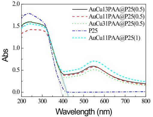
Figure 3.8 TEM images of AuCu13@P25PP(1). ... 83 Figure 3.9 Diffuse reflectance UV-Vis spectra of the modified photocatalysts and
pure P25. ... 85
Figure 3.10 Evolution of UV-Vis absorption spectra of RhB in photocatalytic reaction
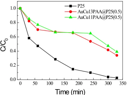
with (a) AuCu13PAA@P25 (1), and (b) AuCu13PAA@P25(0.5) under UV illumination, optical path 2mm, (c) time runs of RhB relative concentration in photodegradation in the presence of pristine and modified P25 under UV illumination. ... 87
Figure 3.11 Time runs of phenol relative concentration in photodegradation in the
presence of pristine P25, AuCu13PAA@P25(0.5), and AuCu11PAA@P25(0.5) under UV illumination. ... 88
Figure 3.12 UV-vis absorption spectra of RhB degraded under visible light in the
presence of (a) AuPAA@P25(1), (b) AuCu31PAA@P25(1), (c) AuCu11PAA@P25(1),
(d) AuCu13PAA@P25(1). Optical path: 2 mm; illumination, λ > 450 nm;
photocatalyst suspended 1 g/L. ... 89
Figure 3.13 Time runs of RhB relative concentration in photodegradation with no
photocatalyst (solid square ■), P25 (solid circle ●), AuPAA@P25(1) (solid triangle ▲), AuCu31PAA@P25(1) (empty square □), AuCu11PAA@P25(1) (empty circle ○), AuCu13PAA@P25(1) (empty triangle △). The initial concentration of RhB is 10-4 M; illumination λ > 450 nm; optical path: 2 mm. ... 91
Figure 3.14 Wavelength shifts of the absorbance maxima in photocatalytic
degradation of RhB with no photocatalyst (B, solid square ■), P25 (C, solid circle ●), AuP25PAA@P25(1) (D, solid triangle ▲), AuCu31PAA@P25(1) (E, empty square □), AuCu11PAA@P25(1) (F, empty circle ○), AuCu13PAA@P25(1) (G, empty triangle △); illumination, λ > 450 nm. ... 91
Figure 3.15 Evolution of UV-Vis spectra of RhB photodegraded in the presence of the
sample (a) AuCu11PP@P25(1), and (b) AuCu13PP@P25(1) under visible light. Illumination > 450 nm, optical path: 2 mm. ... 92
Figure 3.16 (a) Evolution of the UV-Vis spectra of RhB photodegraded in the
courses of RhB relative concentration and wavelength changes of absorbance maxima in photocatalytic degradation of RhB in the presence of the sample AuCu13PAA@P25(1) (square), and after wash-treatment with water (circle). ... 93
Figure 3.17 DRS-TGA of the sample (a) AuCu31PAA@P25(0.5), (b)
AuCu11PAA@P25(1), and (c) AuCu13PAA@P25(1). ... 94
Figure 3.18 Evolution of UV-Vis spectra of RhB photodegraded in the presence of the
sample (a) AuCu31P25PAA(0.5) after calcination, (b) AuCu11P25PAA(1) after calcination, and (c) AuCu13P25PAA(1) after calcination. Illumination > 450 nm. Optical path: 2 mm... 95
Figure 3.19 TEM images of metallic nanoparticle modified P25 and the
corresponding size distributions of the supported metallic NPs (a, b) Au/P25, (c, d) AuCu11/P25, and (e, f) AuCu13/P25. ... 98
Figure 3.20 UV-vis spectra of the colloid (a) AuPAA, (b) AuCu13PAA, (c)
AuCu31PAA, the supernatant of (d) Au/P25, (e) AuCu11/P25, (f) AuCu31/P25 and the solution of (g) PVA (0.1 M), and (h) PAA and PVA (0.1 M of each). ... 99
Figure 3.21 TEM images of (a) Au/P25, (b) AuCu11/P25, and (c) AuCu13/P25 at a
high magnification, all the samples are without thermal treatment and H2 reduction.
... 100
Figure 3.22 DRS spectra of pure P25 and the modified samples with thermal
treatment. ... 101
Figure 3.23 DRS spectra of pristine and modified P25 without thermal treatment. . 102 Figure 3.24 (a) N2 adsorption-desorption isotherms for the sample AuCu13/P25. Inset:
BET surface area plot, (b) the corresponding pore size distribution. ... 104
Figure 3.25 The time runs of relative RhB concentration in photodegradation in the
presence of pristine and modified P25 under (a) UV, and (b) visible illumination. .. 105
Figure 3.26 Histogram of rate constants of the first-order kinetic of RhB or phenol
photodegradation in the presence of pristine and modified P25 under UV light. ... 106
Figure 3.27 The time runs of relative RhB concentration in photodegradation in the
presence of pristine and modified P25 under (a) UV, and (b) visible illumination without thermal treatment. ... 107
Figure 3.28 TRMC signals of pristine and the modified P25 Au/P25, AuCu11/P25
and AuCu13/P25 after thermal treatment. ... 108
Figure 3.29 TRMC signals of pristine P25 and the modified P25 Au/P25,
AuCu31/P25, AuCu11/P25 and AuCu13/P25, without thermal treatment. ... 109
Figure 3.30 UV-Vis absorption spectra of (a) AuCu1:1/P25DPU supernatant before
solution, (d) 1.25×10⁻⁴ M of Cu solution, and (e) 2.5×10⁻² M of urea solution after water bath at 90 °C for 2 hours. Optical path: 10 mm. ... 112
Figure 3.31 UV-Vis absorption spectra of (a) supernatant of Au/P25DPU after
irradiation, (b) 2.5×10⁻⁴ M of Au solution, and (c) 2.5×10⁻² M of urea solution after water bath at 90 °C for 2 hours. Optical path: 10 mm. ... 113
Figure 3.32 UV-Vis absorption spectra of (a) the supernatant of Cu/P25DPU before
irradiation, (b) supernatant of Cu/P25DPU after irradiation, (c) 2.5×10⁻⁴ M Cu solution, and (d) 2.5×10⁻² M of urea solution after water bath at 90 °C for 2 hours. Optical path: 10 mm... 113
Figure 3.33 UV-Vis absorption spectra of (a) supernatant of AuCu13/P25DPU before
irradiation, (b) supernatant of AuCu1:3/P25DPU after irradiation, (c) 1.25×10⁻⁴ M of Au solution, (d) 1.25×10⁻⁴ M of Cu solution, and (e) 2.5×10⁻² M of urea solution after water bath at 90 °C for 2 hours. Optical path: 10 mm. ... 114
Figure 3.34 UV-Vis spectra of Au/P25DPU supernatants before and after several
filtration cyclings. Optical path: 10 mm. ... 114
Figure 3.35 TEM and HR-TEM images of (a,b) Au/P25DPU, (c,d)
AuCu1:1/P25DPU, (e,f) AuCu1:3/P25DPU. Dose rate: 170 Gy/min, dose in total: 20 kGy. ... 116
Figure 3.36 Top. HAADF-STEM image of AuCu1:1/P25DPU (left) and the
corresponding Energy Dispersive X-ray Spectroscopy line scan across an Au/Cu1:1 nanoparticle (right. The The profile was taken along the purple line, the blue line corresponds to CuK and the red one to AuL signal). Bottom. Mapping EDS analysis performed at a metallic nanoparticle of AuCu1:1/P25DPU. ... 118
Figure 3.37 (a) Diffuse reflectance UV-Vis spectra of the modified photocatalysts and
P25, and (b) the plot of transformed Kubelka-Munk function versus the energy of incident light, inset is the partial enlarged view. ... 120
Figure 3.38 (a) XPS survey spectrum and (b) Cu2p region of the XPS spectra of
sample AuCu1:3/P25DPU. The inset in b is Auger CuLMM spectrum of the sample. ... 121
Figure 3.39 Cu2p region of the XPS spectra of sample AuCu1:3/P25DPU, after
photocatalytic reaction under UV illumination. The inset is Auger CuLMM spectrum of the sample. ... 122
Figure 3.40 (a) N2 adsorption-desorption isotherms for the sample AuCu1:3/P25DPU.
Inset: BET surface area plot of, (b) the corresponding pore size distribution. ... 123
Figure 3.41 UV-vis absorption spectra of MO in photodegradation under UV
illumination with the sample AuCu1:3/P25DPU. ... 124
kinetics in photodegradation under UV illumination in the presence of P25 (filled square), Au/P25DPU (filled circle), AuCu1:1/P25DPU (filled triangle), AuCu1:3/P25DPU (open square), Cu/P25DPU (open circle), and no photocatalyst (open triangle). ... 126
Figure 3.43 Rate constants of the first-order kinetic of MO photodegradation under
UV illumination with, (a) P25, (b) Au/P25DPU, (c) AuCu1:1/P25DPU, (d) AuCu1:3/P25DPU, and (e) Cu/P25DPU. ... 127
Figure 3.44 UV-vis absorption spectra of (a) the supernatant of Au/P25DP, and (b)
1.25×10⁻⁴ M HAuCl4 solution. Optical path: 10 mm. ... 129
Figure 3.45 TEM images of the photocatalysts (a) Au/P25DPU-s, (b)
AuCu1:3/P25DPU-s, (c) Au/P25DP at dose rate of 20 Gy/min; and (d) Au/P25DP at dose rate of 170 Gy/min. ... 130
Figure 3.46 The time runs of RhB concentration in photodegradation under (A) UV,
and (B) visible light with (a) P25, (b) Au/P25DPU-s, (c) AuCu1:3/P25DPU-s, (d) Cu/P25DPU-s, and (e) no photocatalyst. ... 131
Figure 3.47 The time runs of RhB concentration in photodegradation under (A) UV,
and (B) visible light with (a) P25, (b) Au/P25DP, (c) AuCu1:3/P25DP, and (d) no photocatalyst. ... 131
Figure 3.48 TEM images of the modified P25 with Au and Cu NPs. (a) Au/P25-T, (b)
AuCu11/P25-T, (c) AuCu13/P25-T, and (d) Cu/P25-T. ... 134
Figure 3.49 Size distributions of Au and Au-Cu NPs deposited on P25 prepared by
chemical method with THPC, (a) Au/P25-T, (b) AuCu11/P25-T, and (c) AuCu13/P25-T. ... 135
Figure 3.50 Size distributions of the modified P25 by chemical method with THPC, (a) Au/P25-T, (b) AuCu11/P25-T, and (c) AuCu13/P25-T. The samples were without
thermal treatment. ... 135
Figure 3.51 HAADF-STEM and BF-STEM images of (a, b) Au/P25-T, (c, d)
AuCu11/P25-T, and (e) AuCu13/P25-T. ... 137
Figure 3.52 Energy dispersive X-ray spectroscopy line scans across external
nanowires of nanoparticles (profiles were taken along the green or violet lines) and corresponding HAADF-STEM images for the samples of (a1, a2) Au/P25-T, (b1, b2) AuCu11/P25-T, and (c1, c2) AuCu13/P25-T. ... 138
Figure 3.53 (a) HAADF-STEM image of AuCu11/P25-T and EDS elemental
mapping analysis at the NPs; (b) EDS analysis of the selected area in a. ... 139
Figure 3.54 Au4f region of the XPS spectra of the sample AuCu1:1/P25 (blue) and
Au/P25 (red)... 140
Cu/P25 (red). ... 141
Figure 3.56 DRS spectra of pure and modified P25 with Au and Cu nanoparticles (a)
thermal treated, (b) without thermal treatment, prepared by the chemical method with THPC. ... 143
Figure 3.57 (a) N2 adsorption-desorption isotherms for the sample AuCu13/P25-T.
Inset: BET surface area plot, (b) the corresponding pore size distribution. ... 144
Figure 3.58 The time runs of phenol, benzoquinone, and hydroquinone concentrations
in photodegradation with pristine P25 under UV illumination. The initial concentration of phenol is 2×10⁻⁴ M (equal to 18.82 ppm). ... 145
Figure 3.59 (a) The time runs of phenol relative concentration in photodegradation
under UV illumination with pure P25, and modified P25, (b) the rate constants of the corresponding photodegradation. ... 146
Figure 3.60 (a) The time runs of RhB relative concentration in photodegradation
under UV illumination with no catalyst, pure P25, and modified P25, (b) the rate constants of the corresponding photodegradation... 148
Figure 3.61 The time runs of phenol relative concentration in photodegradation under
visible illumination with no catalyst, pure P25, and modified P25 without thermal treatment. ... 149
Figure 3.62 TRMC signals of pristine and modified P25 by the chemical method with
THPC. ... 150
Figure 4.1 XRD patterns of (a) the synthesized sample 1, CuO nanowires; (b) the
synthesized sample 2, Cu2O octahedra. ... 162
Figure 4.2 XRD pattern of sample 5. ... 164 Figure 4.3 TEM images of the sample 5 at a lower magnification (a), and a higher
magnification (b). ... 164
Figure 4.4 SEM images of sample 1-4 (a, b, c and d); TEM images of sample 2 (e),
and sample 4 (f); HRTEM image of sample 2 (g) and its corresponding SAED pattern
(h). ... 166 Figure 4.5 TEM images of CuO (a) and Cu2O (b) prepared without SDS, the
experimental conditions are corresponding to sample 1 and sample 2, respectively. 168
Figure 4.6 UV-vis absorption spectra showing the photodegradation of RhB in with
truncated octahedral Cu2O under visible illumination. Optical path: 2 mm. ... 169
Figure 4.7 (a) The time runs of MO concentration and (b) pseudo first-order kinetic
fittings for MO photodegradation in the presence of (i) no catalyst, (ii) CuO nanowires, (iii) Cu2O octahedra and (iv) Cu2O truncated-octahedra under visible
Figure 4.8 SEM images of (a) sample 3, and (b) sample 3 after the photocatalytic
reaction under visible light for 18 minutes. ... 172
Figure 4.9 The plots for MO cycling photodegradation under visible light with the
sample 3. ... 172
Figure 4.10 XRD pattern of the as-prepared CuS NTs, the bottom is the JCPDF card
no. 06-464. ... 175
Figure 4.11 TEM images of as-prepared CuS nanotubes at low magnification (a),
high magnification (b); HRTEM of CuS nanoparticles (c); EDS of as-prepared CuS NTs (d). ... 176
Figure 4.12 FE-SEM images of as-prepared CuS nanotubes at a low magnification (a), and high magnification (b). ... 177 Figure 4.13 (a, b) TEM images and (c. d) SEM images of the synthesized CuS
hollow spheres; the molar ratio of Na2S2O3 to CuCl2 is 3:1. ... 178
Figure 4.14 (a) UV-vis absorption spectra of RhB photodegration by CuS nanotubes
under visible illumination, (b) time runs of relative RhB concentration in photodegradation with CuS (balck squares) and witout catalyst (red circles). Optical path: 2 mm. ... 179
Figure 4.15 UV-Vis absorption spectra of RhB in the adsorption experiment with
prepared CuS NTs in the dark. ... 179
Figure A.1 Picture of the gamma ray source in Radiation Chemistry Laboratory of
USTC. ... 189
Figure A.2 Picture of the gamma ray source in LCP at Université Paris-Sud, Orsay.
... 190
Figure A.3 Schematic illustration of the photocatalytic reaction system A. ... 191 Figure A.4 The LOT-Orien Xenon 300W lamp. ... 191 Figure A.5 Spectral irradiance of LOT-Orien Xenon lamps. ... 192 Figure A.6 Schematic illustration of the cylinder reactor. ... 192 Figure A.7 The Philips TL-8W-840 lamp and its emission spectrum. ... 193 Figure A.8 Picture of XPA-7 photochemical reactor... 194 Figure A.9 Schematic illustration of Model XPA-7 photochemical reactor.[1] ... 194 Figure A.10 UV-visible transmission spectra of (a) visible optical filter, (b) UV
Figure A.11 Scheme of TRMC experimental set-up.[2] ... 196 Figure A.12 Diagram of components of a transmission electron microscope.[4] ... 198 Figure A.13 (a) TEM mass contrast imaging mechanism. (b) TEM diffraction
contrast ... 199
Figure A.14 Schematic of the STEM.[5] ... 201 Figure A.15 A graphic representation of Bragg’s Lawfrom a crystal surface.[6] ... 202 Figure A.16 The principle of photoelectron emission. ... 204 Figure A.17 The classification of the adsorption isotherm. ... 206
General Introduction
Photocatalysis with semiconductors has recently emerged as a promising method for environmental decontamination in water and air treatment. Titanium dioxide (TiO2)
has proven to be the most promising semiconductor photocatalyst not only because of its excellent photoactivity, but also because of its non-toxicity, chemical stability and low cost. However, the fast charge-carrier recombinations and the wide band-gap of TiO2 limit its application under solar light. Hence, many efforts have been devoted to
solve these problems, such as modification with metal nanoparticles or other semiconductors, doping with transition metals or nitrogen and sulfur… In this thesis work, we modified TiO2 with gold and/or copper to enhance its photocatalytic
activity.
Semiconductors with intrinsic band-gap suitable for visible light photocatalysis havealso attracted considerable attention in the past decades. Radiolytic synthesis of copper oxides and copper sulfides with special morphologies and their photocatalytic activity were also investigated in this work.
This manuscript contains four chapters:
The first chapter lays the foundation for this thesis, it will outline several themes. We will make a brief review of various conventional advanced oxidation processes used for wastewater treatment. Basic principles of the photocatalysis processes are described. We will review significant effects on photocatalytic activity of semiconductors. We also will summarize ways to improve the photocatalytic activity. The main deposition methods for semiconductor surface modification will be introduced. The principles of radiolytic synthesis of metal nanoparticles will be presented. We also will describe the research front of non-TiO2 visible light
photocatalysis, and particularly radiolytic synthesis of copper oxides and copper sulfides.
In the second chapter, we describe the experimental conditions, including materials, synthetic protocols for the modification of TiO2 and preparation of copper
compounds, the characterization techniques and the equipments used for the photocatalytic reactions of different model pollutants.
Chapter 3 presents the results obtained for modification of TiO2 with Au, Cu
monometallic nanoparticles or Au-Cu bimetallic nanoparticles by various deposition methods, including colloid deposition by radiolysis, colloid deposition by chemical method, deposition-precipitation method with urea. The photocatalytic properties of the modified TiO2 were studied for degradation of rhodamine B, phenol and methyl
orange under UV and visible light. Time resolved microwave conductivity (TRMC) technique was used to follow the kinetics of excited electrons induced after laser excitation of TiO2. The results of the photocatalytic activities of TiO2 under UV
excitation related to lifetime of the photogenerated charge-carriers are presented. In chapter 4, the radiolytic synthesis of copper oxides and copper sulfides of different morphologies and their photocatalytic activity are presented.
CHAPTER I
FOUNDATION IN
PHOTOCATALYSIS
Chapter 1 Foundation in Photocatalysis
1.1 Water Pollution
In recent years, global environmental pollution has become a serious problem that needs to be solved urgently. The on-going industrialization has been bringing about serious pollution to air and water. Water is essential to our existence. The pollution from both the atmosphere and soil will eventually enter water by deposition and dissolution. Thus, water remediation has emerged as a high national and international priority over the past decades.
Hazardous wastes caused a big threat to water. Both advanced industrialized nations and developing countries encounter tremendous environmental problems related to the remediation of hazardous wastes. The hazardous wastes exist in military installations and civilian effluents. For military installations, problems with hazardous wastes are related to the disposal of hazardous chemicals in lagoons, underground storage tanks, and dump sites. Consequently, the surrounding soil or underlying groundwater aquifers were contaminated with various kinds of hazardous wastes. In the civilian sector, the elimination of toxic and hazardous chemical wastes such as halogenated hydrocarbons from waste effluents and previously contaminated sites has become a major concern.[1] Commonly, general classes of compounds of concern include: volatile organics, chlorinated aromatics, dibenzofuran, dioxins, chlorophenols, chlorinated aliphatic and olefinic compounds, nitrogenous compounds, hydrocarbons, carboxylic acids, alcohols, halocarbons, heteroatom compounds…[2] Besides, aqueous soluble dyes and other aromatic molecules, such as rhodamine B, methyl orange, and phenol etc. are widely used in textile and other industries. These compounds are considerably stable in the environment under natural light.
Conventional methods for elimination of these pollutants are aeration, extraction, high-temperature incineration, filtration, distillation, reverse osmosis, ion exchange, absorption, biological treatment, ozonation, and etc. However, most of the organic compounds are resistant to conventional chemical and biological treatments. The so-called advanced oxidation processes (AOPs) have been reported to be effective for the near ambient
degradation of soluble organic contaminants from waters and soils, because they can contribute to an almost total degradation.[3-4] Of these, advanced oxidation processes (AOPs) will probably constitute the best option in the near future.[5]
1.2 Advanced Oxidation Processes (AOPs)
As defined broadly, AOPs are mainly considered to be the aqueous phase oxidation processes which are based primarily on the oxidizing hydroxyl radical in the mechanism resulting in the destruction of the model pollutants or xenobiotic or contaminant compounds.[5-6]
Highly reactive hydroxyl radicals (HO•) [E0(HO•/H2O = + 2.8 VNHE)] are traditionally
known to be the active species responsible for the decomposition of organic pollutants.[7-8] Owing to their high standard reduction potential of 2.8 V vs NHE (Normal standard hydrogen electrode) in acidic media,[9] these radicals are able to oxidize almost all organic compounds to carbon dioxide (CO2) and water.[10]
AOPs show considerable similarities because of the participation of hydroxyl radicals in most of the mechanisms that are operative during the reaction. Hydroxyl radicals are extremely unstable because of their high reactivity. Considering that the hydroxyl radicals are unstable and reactive, they must be produced continuously in-situ through chemical or photochemical reactions.
Generally, AOPs use photolysis (UV), ozone (O3), hydrogen peroxide (H2O2), ozone in
combination with UV (O3/UV), hydrogen peroxide and UV light (H2O2/UV), ozone plus
hydrogen peroxide (O3/H2O2), Fenton’s reagent (see page 11) and photocatalysis (which is
based on interaction of light with semiconductors).[5, 11-12] Compared to the AOPs based on O3/UV, H2O2/UV, or on photo-Fenton processes (techniques which have been practically
employed to carry out the mineralization of organic compounds), semiconductor-based photocatalysis has also shown a promising potential in organic pollutant degradation in recent years. The various AOPs are described in detail in the following paragraph.
This process is based on excitation of organic molecules by UV irradiation.[5, 13] Direct photolysis involves the interaction of light with molecules—in addition to water—to bring about their dissociation into fragments. It is reported that photolysis can be more effective when UV irradiation is combined with ozone, hydrogen peroxide, homogeneous, heterogeneous catalysis or photocatalysis.[11, 14]
1.2.2
O
3In the O3 AOP, two possible ways of oxidizing action may be taken into account: the
direct way owing to the direct reaction between O3 and the dissolved molecules,[15] and the
radical way (indirect way) because of the reaction triggered by the radicals generated in the ozone decomposition (hydroxyl radicals).[5] Compared to other oxidizing reagents, O3 is
more efficient in organic pollutant degradation. In addition, it is not harmful for most of the organisms. To our knowledge, ozonation has been widely used for drinking water disinfection.[16] However, the limitation of its application in water treatment is due to its high energy consumption.[11]
1.2.3 O
3/UV
Photolytic ozonation (O3/UV process) is an effective means for the oxidation and
destruction of organic pollutants in aqueous solution.[17-19] It has a crucial potential for wastewater treatment. In principle, aqueous systems saturated with O3 are irradiated with UV
light at 253.7 nm. In this case, the extinction coefficient of O3 at 253.7 nm is 3300 M-1 cm-1,
which is much higher than that of hydrogen peroxide.[11] O3/UV process generates HO•
radicals by the light-induced homolysis O3 and the subsequent by the interaction of O (1D)
with water.[20-21] The global reaction is shown in equation 1.1:
310nm
3 2 2
O +H O→hν< 2HO•+O (1.1) O3/UV is more effective for the decomposition of some organic compounds than either
UV or O3 alone.[11] In this O3/UV process, it is worth noting a high synergetic effect between
1.2.4 H
2O
2/UV
This method is based on the formation of HO· radicals by the photolysis of hydrogen peroxide and the subsequent propagation reactions:
2 2
H O + →hν 2HO• (1.2) Irradiation with a wavelength shorter than 400 nm is able to photolyze the H2O2
molecule. The accepted mechanism is the cleavage of the molecule H2O2 into two hydroxyl
radicals. Under UV irradiation (250 nm < λ), the yield of photolysis of aqueous hydrogen peroxide is around 50 times lower than O3. This process needs a relatively large amount of
H2O2 or a much longer UV-exposure time than, for instance, AOP of UV/O3.[11]
Hydroxyl radical can react with H2O2 to generate the hydroperoxyl radical (HOO·),
which is also an oxidative species (equation 1.3). Hydrogen peroxide is also known to decompose to hydroxyl radical by a dismutation reaction with a maximum rate at the pH equal to its pKa value of 11.6 (equation 1.4)
2 2 2
HO•+H O →H O HOO+ • (1.3)
2 2 2 2 2
H O +HO •→H O O+ +HO• (1.4) The generated hydroxyl radical can react with organic pollutants by hydrogen abstraction, electrophilic addition and electron transfer mechanisms. However, the disadvantage of this AOP is the absorption coefficient of H2O2 and quantum efficiency of HO· is very low at
wavelength longer than 250 nm.
1.2.5 O
3/H
2O
2In this process, hydroxyl radicals are generated by a radical-chain mechanism by interaction between O3 and the H2O2.[5, 22-23] Equation 1.5 shows the global reaction:
3 2 2 2
2O +H O →2HO•+3O (1.5)
This AOP is based on the O3/H2O2 process. The efficiency of this process is
tremendously improved by association with UV irradiation. It is considered to be the most effective process for extremely polluted effluents.[24] However, the process is not an economic method.
1.2.7 Fenton’s reagent
In this process, hydroxyl radicals are generated by means of the reaction between H2O2
and iron (II). The overall reaction for the hydroxyl radical generation in acidic solution is shown in equation 1.6:
2 3 2 2
H O +Fe +→Fe++HO•+OH− (1.6) The mechanism for the ferric ion in decomposition of H2O2 in acidic solution to release
hydroxyl radicals has been intensively discussed in former studies.[25]
1.2.8 Photocatalysis
Photocatalysis has proven to be a promising technology for degrading aromatic compounds.[26-29] Compared to the other conventional AOPs discussed above, photocatalysis may be more effective and more economicas the involved semiconductor can continuously catalyze the decomposition of organic pollutants under irradiation. The energy is transformed directly from solar to chemical without consumption of oxidizing reagents. Electron-hole pairs are produced in the semiconductors under irradiation (in most cases UV light). These charged carriers can recombine or migrate to the surface (when they escape from recombination) of the semiconductor creating radicals. Under O2, these radicals can oxidize
most of the organic molecules. The general equation taking place in semiconductors under irradiation is shown as following:
g CB VB
E
Semiconductor ≥hn →Semiconductor (+ e −+h +) (1.7) (hVB+ represents the positive holes, Eg refers to band-gap)
1.3 Photocatalysis for decomposition of organic dyes
Studies on photocatalysis by TiO2 have been reported since the start of 20th century. In
1938, Doodeve and Kitchener reported that photodegradation of dyes by TiO2 occurred both
in vacuum and under oxygen. But at that time, this phenomenon was identified as a mechanism of photo-bleaching.[31] It was also found that TiO2 itself did not change through
the photo-bleaching reaction. However the terminology of “photocatalyst” was not used for TiO2 but it was called a photosensitizer.
After the report of photocatalytic water splitting by Fujishima,[32] there were some studies on other applications of the photocatalytic activity of TiO2 in decomposition of
organic pollutants such as organic dyes . Frank and Bard reported for the first time the decomposition of cyanide in the presence of aqueous TiO2 suspension.[33] A mechanism was
given for this photodecomposition process based on the known procedure on TiO2 electrodes.
The electrons in the conduction band reduce oxygen while the holes in the valence band cause the oxidation of CN–:
VB 2
CN− +2OH− +2h + →CNO−+H O (1.8) And the further oxidation of CNO− is possible. Although the quantum efficiencies here were lower than those found for a single crystal TiO2 electrode coupled to a platinum cathode
in a photoelectrochemical cell, their are still respectable.
In a photodecomposition system which includes the photocatalyst and the organic molecules, photo-induced molecular transformations or decompositions occur at the surface of the catalyst. Depending on where the initial excitation takes place, photocatalysis can be generally divided into two classes of processes:
1) Catalyzed photoreaction. The initial photoexcitation occurs in an adsorbate molecule which then interacts with the ground state catalyst substrate.
2) Sensitized photoreaction. The initial photoexcitation takes places in the catalyst substrate and the photo-excited catalyst then transfer an electron or energy into a ground state molecule, the process is called a sensitized photoreaction.
The initial photoexcitation of the system is followed by subsequent electron transfer and (or) energy transfer. In consequence, chemical reactions in the photocatalysis processes are attributed to the de-excitation processes by electron transfer or energy transfer.
1.4 Rising of Photocatalysis
Fujishima and Honda discovered the photocatalysis in water splitting on TiO2 electrodes
for the first time in 1972, marking the beginning of a new era in photocatalysis.[32] Before, the photocatalytic investigation of TiO2 might have just attracted partially scientists’ attention
in the field of either catalysis or photochemistry. Then, this report on water splitting by TiO2
attracted the attention not only of electrochemists but also of many scientists in a broad area, and study of photocatalysis by TiO2 is now developing widely in both academic and industrial
society.[34] The application of photocatalysis in the fields of polluted water treatment, solar- to chemical energy conversion via water splitting (hydrogen generation) and CO2 reduction
into light hydrocarbons are attracting much attention.[35]
V
+ -hv 1 2 3 4 4 5 6Figure 1.1 Schematic diagram of photoelectrochemical cell. (1) n-type TiO2 electrode; (2)
platinum black counter electrode; (3) ionically conducting separator; (4) gas buret; (5) load resistance; and (6) voltmeter. From ref. [32]
Figure 1.1 gives the schematic diagram of a photoelectrochemical cell designed by
Fujishima for water splitting. A single crystal wafer of n-type TiO2 (rutile) was employed as
anode while the platinum black as the cathode. Both of the electrodes were submerged in an aqueous electrolyte of pH 4.7. The TiO2 anode was connected to a platinum black electrode
with copper lead wire through an external load resistance. An ionically conducting separator was placed between the two basins to segregate the electrolytes. When the surface of the TiO2
electrode was irradiated with light consisting of wavelengths shorter than 415 nm, that is 3.0 eV, which corresponds to the band gap of TiO2, a photocurrent flowing from the platinum
positive electrode to the TiO2 negative electrode was detected by the voltmeter. The direction
of the current gave the evidence that the oxidation half reaction (oxygen evolution) occurs at the TiO2 electrode and the reduction half reaction (hydrogen evolution) takes place at the
platinum black electrode.
To show more details, the two half reactions at the anode and the cathode were featured on one particle-based TiO2 molecule combined with platinum particles. It can be seen from
Figure 1.2 that an electron is transferred from valence band into conduction band, excited by
the energetic UV photons. In the meanwhile, a positive hole which has a high oxidation potential was produced in the valence band and it is able to drive the oxidation of H2O to O2
and H+. The excited electron moved to the platinum particle because the Fermi energy level of platinum is lower than that of conduction band of TiO2. Finally, hydrogen was generated from
the H+ reduction by the excited electrons on the surface of the platinum electrode.
It must be figured out that there are two indispensable requirements for the thermodynamically favorable water-splitting reaction; the first one is that the conduction band should have higher energy than the hydrogen-evolution potential and the second one is that the valence band should be lower than the oxygen-evolution potential.
By UV irradiation of TiO2, it is then possible to decompose water without employing any
external voltage, according to the following equations:
2 TiO +2hν→2e−+2h+ (1.9) 2 2 1 2 H O O 2 H 2 h+ + → + + (1.10) 2e− +2 H+ → (1.11) H2 (h+ refers to the hole) So, the overall reaction is:
2 2 2
1
H O 2 O H
2
+ hν→ + (1.12)
When semiconductor photocatalysts are used in organic pollutant degradation, the redox potential of the generated holes should be sufficiently positive to produce hydroxyl radicals. Furthermore, the redox potential of the electrons must be negative to be able to reduce adsorbed O2 to superoxide (O2–
.
).[36-37] The hydroxyl radical can be generated by the reaction of oxidative holes with surface adsorbed water (H2O) or hydroxyl anions. It has such
a strong oxidizing activity that it breaks down the aromatic structure of organic pollutants into a variety of intermediate products and finally to inorganic molecules like H2O, CO2 etc.
According to the discussion above, these two half reactions in photocatalysis could be used to solve not only the problem of energy shortage, but also to treat the serious environmental pollution.
Figure 1.2 Scheme of water splitting process in a particle-based semiconductor catalyst linked with a platinum particle.
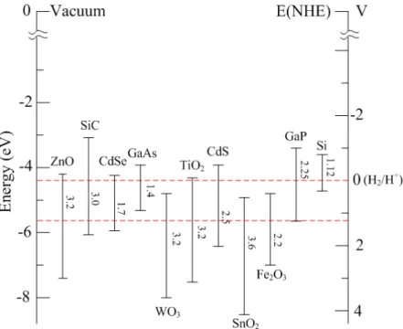
Figure 1.3 CB and VB positions for various semiconductors in aqueous electrolytes at pH = 1.
1.4.1 Band-gap Positions
The VB and CB positions of a range of semiconductors including oxides, non-oxides and elemental Si are presented in Figure 1.3. A potential scale (V) versus the normal hydrogen electrode (NHE) is presented on the right side and the internal energy scale is given on the left for comparison to the vacuum level. Redox potentials for the water-splitting half-reactions versus the NHE are also indicated with dashed red lines. From the scheme, we can see that for the water-splitting reaction to take place without external potential application, the band-gap should straddle these redox potentials, that means that the CB should have higher energy (more negative potential) than the hydrogen evolution potential while the VB should be lower than the oxygen evolution potential.
Although the band-gap energy is a significant property for photocatalysis. the ability of a photocatalyst to absorb visible and/or UV light is the crucial factor, but other properties have also to be considered such as: the photocatalyst should be also i) chemically and biologically inert and photostabe, ii) nontoxic, and iii) inexpensive. The semiconductors TiO2, ZnO, CeO2,
SrTiO3, WO3, Fe2O3, Bi2S3, GaN, CdS and ZnS can all act as photoactive materials for
by a filled valence band and an empty conduction band. Among these semiconductors, TiO2 is
the most widely used photocatalytic material because it fulfills all of the above requirements as well as exhibiting adequate conversion values.[36, 38] TiO2 has many advantages such as it
has high photon harvesting performance in UV light region; it widely exists on the earth and exhibits an extremely chemical stability; it is biologically inert and non-toxic; moreover, it is cheap and easy to synthesize. In this thesis, one part of the work is surface modification of TiO2 to enhance its photocatalytic activity under UV and visible illumination.
1.5 Basic Principles in the Photocatalysis Process
1.5.1 Semiconductor Photoexcitation
Originally, when a semiconductor is irradiated with light with sufficient energy (larger than the band gap), photochemical processes occur in the semiconductor (Figure 1.4). As shown in the insert, an electron is excited from the valence band to the conduction band, forming a positive hole in the valence band. Just after that, recombination of the generated electron-hole pairs takes place in the core of semiconductor (trace a). Some electron-holes can escape from recombination and migrate to the surface of the semiconductor, and finally can recombine with each other (trace b) or react with the species at the surface. Besides, recombination also occurs on the surface between the electron-holes in-situ generated on the surface. The electron-holes on the surface can either react with electron acceptor (trace d) or electron donor (trace c). These two paths are examples of direct reactions between the semiconductor and the adsorbate (electron donor or acceptor). While the recombination in trace a and b results in luminescence. These pathways illustrate the fundamental processes of photocatalysis in a semiconductor.
+ - + + -+ + Valence band Conduction band Volume recombination Surface recombination
h
ν
A A– D D+ a b c dFigure 1.4 Photochemical processes in a semiconductor followed by deexcitation events. Where A is electron acceptor and D is electron donor. From ref. [39]
1.5.2 Characteristic Times
The general mechanism for the heterogeneous photocatalysis on TiO2 on the basis of
laser flash photolysis measurements has been proposed by Hoffman et al.[1] A succession of photochemical processes takes place in the volume and on the surface of the solid. Figure 1.5 shows the scheme of characteristic times in the photocatalysis processes, where the photoreactions are initiated from the charge-carrier generation. The absorption of a photon occurs very rapidly, on the order of 10-15 s.[39]
Then, the charge-carrier trapping occurs, including electrons trapping and holes trapping. The >TiOH in the equations represents the primary hydrated surface functionality of TiO2.[1,
40] {>Ti4+OH·} is the surface-trapped VB hole (hydroxyl radical), and {>Ti3+OH} is the surface-trapped CB electron. The eq. 1.15 represents a dynamic equilibrium indicating a reversible trapping of CB electrons in a shallow trap below the CB edge. So, there is a finite probability that e- could transfer back into the CB at room temperature.
From this characteristic times scheme, we could clearly conclude that the two routes to enhance the photocatalytic activity are: i) increasing of charge-carrier yields, ii) trapping the charge-carrier to postpone their recombination.
Figure 1.5 Scheme of characteristic times in the photocatalysis process. a) Charge-carrier generation: 2 VB CB TiO →hν h + +e − fs (1.13) b) Charge-carrier trapping. Fast trap hVB+ + >Ti OH4+ → >
{
Ti OH4+ •}
+ 10 ns (1.14) Shallow trap eCB−+ >Ti OH4+ ↔ >{
Ti OH3+}
100 ps (1.15) Deep trap eCB−+Ti4+→Ti3+ 10 ns (1.16) c) Charge-carrier recombination slow recombination{
4}
4 CB e − + >Ti OH+ • +→ >Ti OH+ 100 ns (1.17) fast recombination hVB+ +{
>Ti OH3+}
→ >Ti OH4+ 10 ns (1.18) d) Interfacial charge transfer.slow
{
4}
4Ti OH+ • + D Ti OH+ D•+
> + → > + 100 ns (1.19) very slow e− + → >A Ti OH4+ +A•− ms (1.20)
1.5.3 Quantum Efficiency (QE)
The efficiency of the photocatalytic process is measured by a quantum yield which is defined as the number of events occurring per absorbed photon. In the case of a photodecomposition reaction, the quantum yield (Φ) is defined as the ratio of the amount of molecules decomposed over that of photons absorbed. It is very difficult to measure the actual absorbed light in heterogeneous systems because of the scattering of light by the semiconductor surfaces. However, it is generally assumed that all the light is absorbed and the efficiency is quoted as an apparent quantum yield. Sometimes the QE is measured as the yield of a particular product in spite of several products produced in the photocatalytic reactions. The QE for an ideal system follows the simple relationship below:
CT CT R
=
Φ k+
k k (eq. 1.21)
In this equation 1.21, kCT represents the rate of charge transfer, and kR refers to the rate of
the electron-hole recombination.
1.5.4 Recombination Effects
Apparently, a semiconductor with a lower band-gap is able to absorb more photons in the visible region, which would lead to a better photocatalytic activity under sunlight. In fact, there are many semiconductors with low band-gap energy in the visible region, such as GaAs (Eg is around 1.4 eV) shown in Figure 1.3. However these semiconductors are not efficient in photocatalysis. One of the main reasons for their poor photocatalytic performance is the high recombination rate of their generated electron-hole pairs. The recombination effect could scavenge the electron-hole pairs and thus lower the possibility of electron-hole transfers from the semiconductor to the adsorbed molecules. This effect dominates in many of the semiconductors with small band-gap energies over electron-hole transfer making these semiconductors inefficient.
Obviously, electron-hole recombination is detrimental to the efficiency of a semiconductor photocatalyst. Therefore, modifications of semiconductor surface such as
deposition of metal, doping, or combinations with other semiconductors can be beneficial in decreasing the electron-hole recombination rate and thereby increasing the quantum efficiency of the photocatalysts.
1.6 Ways to enhance the photocatalytic activity
1.6.1 Quantum size effects
The size of the semiconductor particles can have an effect on the band-edge positions; these are known as quantum size effects. Quantum size effects occur for semiconductor particles on the order of 10-100 Å in size. The anomalies arise when the size of the semiconductor particles become comparable to the de Broglie wavelength of the charge-carriers in the semiconductor. These effects could increase the band-gap of the semiconductors as the nanoparticle size gets smaller and smaller. Figure 1.6 illustrates the increases in band gap for CdS and CdSe when the particle size decreases. For CdS, the band-gap dramatically increases from its characteristic value for the bulk CdS of ~2.6 eV to 3.0 eV for the particles in the order of 26 Å in size. In the case of CdSe, the band-gap increases by 0.32 eV as the particle size decreased from 4.2 nm to 2.8 nm. The more positive valence band implies an increased oxidizing capability of the holes. As well, the more negative conduction band means an enhancement on reducing capability of the generated electrons.
Figure 1.6 Quantum size effect on semiconductor band-gap of (a) CdS, and (b) CdSe and metal oxides. [39, 41]
confinement of electron and hole in a potential well of small geometrical dimensions. The confinement produces a quantization of discrete electronic states and thus increases the effective band gap of the semiconductor.[39, 42-43]
These changes on the band-edge positions of the valence band and the conduction band influence the photocatalytic properties of the semiconductor, providing an interesting yet challenging aspect to the design of novel photocatalysts.
1.6.2 Metal Semiconductor Modification
Semiconductors can be modified by deposition of metal particles on their surface. The metal that modifies TiO2 does not form part of the crystalline framework, but exists in a
separate phase in interfacial contact with TiO2 particles. In order to obtain stable and durable
materials, the metal used in this approach should be chemically inert. Based on this, noble metals are most suitable for this purpose.
In the past decades, various metals such as Au, Ag, Pt, Pd, Rh, Ni, Co, Ir, and Cu were used to modify the surface of TiO2 or other substrates.[44-54] The modification with metal
nanoparticles (NPs) can result in an enhancement in photocatalytic activity under UV illumination. The approved interpretation is that the metal NPs act as electron traps, which can decrease the electron-hole pair recombination rate, consequently prompt the holes to diffuse to the semiconductor surface where oxidation of organic species can occur. The scheme of the electron trapping by deposited metal NPs is illustrated in Figure 1.7. This mechanism was confirmed by time resolved microwave conductivity (TRMC) measurements, where a reduction in the photoconductance was observed for the semiconductor excited with UV laser.[50] Takai et al. used methylene blue (MB) as an indicator to prove the electrons were stored in the TiO2 supported Ag NPs.[55] Moreover, modification with bimetallic NPs
can result in better catalytic activity compared to the monometallic ones, ie. Ag-Au[35, 56-57], Au-Cu,[58-61] and Pt-Au [48] modified titania. We have shown in this work that the bimetallic Au-Cu alloyed nanostructures were more efficient in electron scavenging than the monometallic Au and Cu ones.[62]
Figure 1.7 Schematic illustrations of (a) photo-excited metal-modified semiconductor particle, and (b) RhB degradation under UV irradiation on Pt cluster modified TiO2. [39, 50]
There are different mechanisms proposed to explain the enhancement caused by modification with plasmonic metal NPs under visible illumination. Plasmonic metal nanostructures are characterized by their strong interaction with resonant photons through an excitation of surface plasmon resonance (SPR). SPR can be described as the resonant photo-induced collective oscillation of surface electrons, established when the frequency of photons match the intrinsic frequency of surface electrons oscillating against the restoring force of positive nuclei.[63] The first view, most commonly, is that incident photons are absorbed by metal NPs injecting electrons into the conduction band of TiO2.[64-69] The
metallic plasmonic NPs (mainly Au, Ag, Cu which have a plasmon resonance in the visible range) essentially act like a dye sensitizer, absorbing resonant photons and transferring the excited electron to the nearby semiconductor particle (Figure 1.8). Besides, the electron transfer implies that plasmon activation of metal particles on semiconductor particles by visible light generates positive charges on the metal particles and conduction-band electrons on the semiconductor particles. The oxidation and reduction reactions occur simultaneously as with conventional photocatalysts activated by UV-light.[39, 70] Because of the excellent mobility of charge-carriers and high absorption cross-sections, which is up to 105 larger than the cross-section of typical dye sensitizer molecules, plasmonic nanostructure of noble metals represent very promising sensitizers.[71] Another advantage for the noble metal NPs is that they are very stable under light compared to dye sensitizers.
Tsukamoto et al. put forward a new idea on the charge transfer mechanism.[70] It is that the joint active site consisting of Au/anatase/rutile phases facilitates smooth e– transfer from the photoactivated Au NPs to TiO2 (Figure 1.9). In a system of anatase/rutile modified with
Au NPs, a) plasmon activation of gold NPs transfers e– to the tightly bound rutile; b) e– then move to well-conjugated anatase; and c) O2 is reduced there by e–. Usually, e– transfer from
rutile to anatase is thermodynamically unfavorable because the conduction band potential (ECB) of rutile (-0.05 V vs NHE) is less negative than the ECB of anatase (-0.25 V).[72]
However, the e– injection from Au NPs to rutile accumulates e– in its conduction band and contributes to the negative shift of ECB (Figure 1.9b).[73-75] As a result, the consecutive e–
transfer from Au particles to rutile and then to anatase leads to a photoactivity under visible irradiation.
Figure 1.8 Mechanism of SPR-induced charge transfer. (i) electrons near the metal Fermi level, Ef are excited to surface plasmon states; (ii) the electrons transfer to a nearby
semiconductor particle; (iii) this activates electron-driven processes such as the hydrogen-evolution half-reaction.[63]
Besides the charge injection mechanism, near-field electromagnetic mechanism was also proposed to interpret SPR-induced enhancements in the photocatalytic activity of semiconductors on systems where the semiconductor and the plasmonic metal were separated from each other by thin, non-conductive spacers preventing any direct charge exchange between the two building blocks.[76-78] This mechanism is based on the interaction of the
semiconductor with the strong SPR-induced electric fields localized nearby at the metallic nanostructure. The electric fields close to plasmonic nanostructures (a few nanometers) are orders of magnitude higher than the field of incident photons. Photo-excited plasmonic nanostructures essentially play a role of concentrators that can amplify the local light intensity. As the rate of electron-hole formation in a semiconductor is proportional to the local intensity of the electric field (more specifically |E|2),[79-80] the electron-hole generation in some regions of the semiconductor increases by a few orders of magnitude (even grow out of nothing when the light energy is not sufficient to excite the semiconductor).
Figure 1.9 Proposed mechanism for Aerobi oxidation of Alcohol on the Au/P25 catalyst under visible light illumination.[70] (P25 is a commercial TiO2 that is a mix of anatase and rutile)
1.6.3 Composite Semiconductors (Semiconductor Modification)
Coupled semiconductor photocatalysts provide an available way to increase the photocatalytic efficiency by extending the light absorption range, or by increasing the charge-carriers separation. Serpone et al. reported for the first time that coupling of the semiconductors CdS and TiO2 led to significant enhancement in efficiency of the
photocatalytic process.[81-82] Figure 1.10 illustrates the photoexcitation process for the composite semiconductors CdS-TiO2. A photo-excited electron can be injected from the
valence band of CdS into the conduction band of TiO2 while the holes remain in the VB of
![Figure 3.2 Evolution of UV-Visible absorption spectra with irradiation time of irradiated HAuCl 4 /CuCl 2 solutions containing PAA (0.1 M) and 2-propanol (0.1 M) (a) AuCu13PAA, [HAuCl 4 ] = 5×10 -4 M, [CuCl 2 ] = 1.5×10 -3 M, (c) AuCu11PAA, [HAuCl 4 ]](https://thumb-eu.123doks.com/thumbv2/123doknet/14525296.722907/100.892.145.743.239.956/evolution-visible-absorption-irradiation-irradiated-solutions-containing-propanol.webp)

![Figure 3.6 Evolution of UV-Vis absorption spectra of the sample (a) AuCu31PP, [HAuCl 4 ] = 1.5×10 -3 M, [CuCl 2 ] = 5×10 -4 M, (b) AuCu11PP, [HAuCl 4 ] = 10 -3 M, [CuCl 2 ] = 10 -3 M, (c) AuCu13PP, [HAuCl 4 ] = 5×10 -4 M, [CuCl 2 ] = 1.5×10 -3 M, a](https://thumb-eu.123doks.com/thumbv2/123doknet/14525296.722907/104.892.140.745.250.719/figure-evolution-absorption-spectra-sample-haucl-haucl-haucl.webp)