Seebeck coefficient in multiphase thin films
12
0
0
Texte intégral
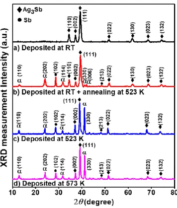
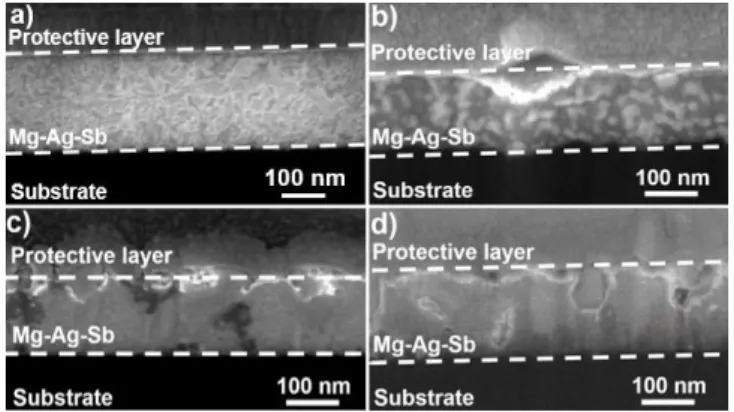
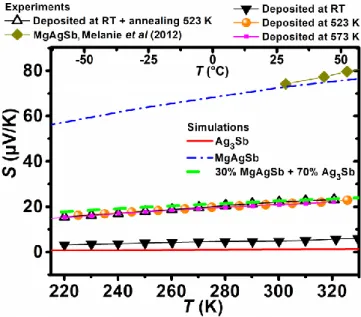
Figure
Documents relatifs