Degradation of vertical GaN-on-GaN fin transistors:
Step-stress and constant voltage experiments
The MIT Faculty has made this article openly available.
Please share
how this access benefits you. Your story matters.
Citation
Ruzzarin, M. et al. "Degradation of vertical GaN-on-GaN fin
transistors: Step-stress and constant voltage experiments."
Microelectronics Reliability 88-90 (September 2018): 620-626 ©
2018 The Authors
As Published
http://dx.doi.org/10.1016/j.microrel.2018.06.044
Publisher
Elsevier BV
Version
Final published version
Citable link
https://hdl.handle.net/1721.1/121546
Terms of Use
Creative Commons Attribution-NonCommercial-NoDerivs License
Contents lists available atScienceDirect
Microelectronics Reliability
journal homepage:www.elsevier.com/locate/microrel
Degradation of vertical GaN-on-GaN
fin transistors: Step-stress and constant
voltage experiments
M. Ruzzarin
a,⁎, M. Meneghini
a, C. De Santi
a, M. Sun
b, T. Palacios
b, G. Meneghesso
a, E. Zanoni
aaDepartment of Information Engineering, University of Padova, via Gradenigo 6/b, 35131 Padova, Italy bMassachusetts Institute of Technology, Cambridge, MA 02139, USA
A R T I C L E I N F O Keywords: Vertical transistors GaN Stability Degradation Reliability A B S T R A C T
We present an extensive analysis of the degradation of GaN-on-GaNfin-vertical transistors submitted to stress under positive gate voltage and off-state conditions. By analysing the degradation kinetics we demonstrate the existence of different processes: (i) trapping of electrons in the gate insulator under positive gate bias, (ii) time-dependent breakdown of the gate MOS structure under forward gate voltage; (iii) catastrophic failure for o ff-state voltages higher than 280 V. 2D simulations are used to identify the physical location of the failed region, and to investigate the dependence of electricfield on fin width (values between 70 nm, 195 nm and 280 nm).
1. Introduction
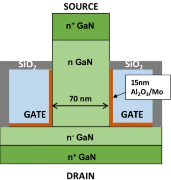
Vertical GaN devices have recently demonstrated to represent an excellent alternative to lateral transistors [1,2]. In fact, they allow to reach high power densities (compared to lateral devices), and break-down voltages in the kV range [3,4]. An interesting device structure is the Vertical Fin Field Effect Transistor (VFET). These devices are based on a fin-architecture, where current flows through nanometer-sized channels having a MOS stack on the sides (seeFig. 1). VFETs are pro-mising for power electronics, since they can reach high breakdown voltages (in excess of 1000 V) [5], in a reduced die area in comparison to lateral topology [6]. In addition, VFETs offer excellent performance
(0.36 mΩ cm2) [7] without the need of a p-GaN layer or epitaxial
re-growth, thus simplifying the fabrication process compared to other vertical structures such as the CAVET [3] and the trench-MOSFET [4]. Despite the great potential of vertical GaN transistors, the stability and reliability of these devices has not been investigated in detail so far [8,9].
The aim of this paper is to present a detailed analysis of the de-gradation of VFETs submitted to forward gate voltage and high drain bias in OFF state. We demonstrate the following original results: (i) when the devices are submitted to stress at high gate voltage, a positive shift of the threshold voltage (VTH) is induced for VGS≥ 3.5 V. Such
effect is ascribed to the injection of electrons from the channel to the gate insulator. (ii) When the devices are submitted to prolonged stress at positive bias (VGS= 5 V, VD= VS= 0 V), they reach the failure
through dielectric breakdown. 2D simulations indicate that the failure
point is located at the corner of the insulator, where the electricfield is maximum. (iii) Step stress tests performed in OFF-state with high drain bias show a soft failure for VDstress= 200 V, followed by a catastrophic
failure for voltages higher than 280 V. The simulation of the electric field for high drain bias for three GaN different fin width demonstrates that the maximum electricfield occurs at the corner of the dielectric and it is higher for devices with shorterfin width. The results described within this paper provide relevant information for the development of reliable vertical transistors based on GaN.
2. Device structure
The cross section of tested devices is shown inFig. 1. The epitaxial-structure was grown by IQE by metal-organic chemical vapor deposi-tion (MOCVD) on 2 inch bulk GaN substrates. It consists of a 0.2μm lightly n-doped GaN layer, a 8μm n-doped GaN drift layer, and a 0.3 μm heavily-doped GaN cap layer. In the devices studied in this paper, 56 GaN channel layers (width = 70 nm and 280 nm) operate in parallel. Current control is obtained thanks to a MOS structure (metal = mo-lybdenum, insulator = Al2O3) on the sidewall of each fin. For
VGS> 1 V, a channel is formed (through accumulation) at the GaN/
oxide interface, and current canflow vertically. The total active area considered is 9600μm2.
⁎Corresponding author.
3. Results
3.1. Forward gate stress
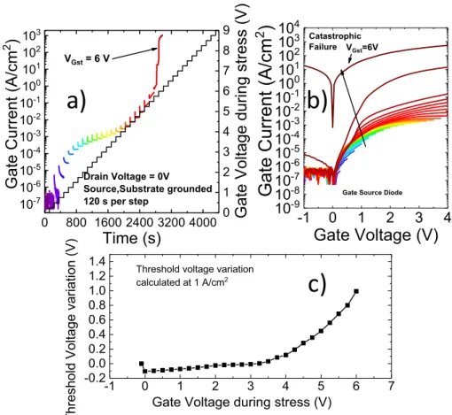
InFig. 2the results of the step stress analysis under positive gate bias for device with 70 nm offin width are reported. By applying low gate voltages of stress (VGS< 5.5 V) we observe an increase in gate
current during stress (Fig. 2(a)). An abrupt increase in the gate current
is observed for VGS> 5.5 V, the catastrophic failure is reached at
VGS= 6.75 V. By looking at the various phases of the step-stress
ex-periment inFig. 2, we observe the existence of different stress regimes: 1) For VGstress= 0.5 V (first two steps inFig. 2), the gate current
de-creases during stress, due to slight trapping of electrons inside the insulator.
2) For 0.75 V < VGstress< 2.25 V (Fig. 2), we observed a fast initial
decrease in the gate current (trapping of electrons in the oxide), followed by an increase. Such increase could be ascribed to a partial-de-trapping of electrons due to the increasing electricfield. 3) For 2.25 V < VGstress< 4.5 V (Fig. 2), an additional (slight)
de-crease in gate leakage is observed, at the end of each stage of the step-stress test. This can be related to the creation of defects inside the oxide, which leads to a stronger electron trapping. The newly trapped electrons have a repulsive action, prevent further electrons from being trapped under in the oxide, thus inducing a decrease/ stabilization in gate leakage.
4) Exposure to high electricfields leaks to the creation of percolation/ shunt paths and to the consequent breakdown of the dielectric, for VGstress> 5.5 V
Changes in the performance of the device under test are investigated by monitoring the I-V characteristics after each step of stress (0.25 V), the plot of the gate-source diode curves is reported inFig. 2(b). As can be noticed, higher stress voltages induce an increase gate leakage, confirming that stress is inducing a generation of defects within the oxide. The IDVG plot performed after each step of stress (Fig. 3(a))
shows that for VGS> 3.5 V the VTHshifts towards more positive values
(Fig. 3(b)). This mechanism can be ascribed to the injection of electrons from the accumulation layer in the GaN channel into the gate dielectric in agreement with the abrupt initial decrease in the gate current during the step stress (Fig. 2(a)).
We tested in the same step stress test a device with same structure as in (Fig. 1) and wider channel width (280 nm). The gate current (Fig. 4(a)) increases by increasing the stress voltage. We observe the
n
+GaN
n GaN
n
-GaN
70 nm
GATE
GATE
15nm
Al
2O
3/Mo
SiO
2SiO
2n
+GaN
Fig. 1. Structure of the tested device: the cross section of one GaN channel (width = 70 nm) is reported.
-1
0
1
2
3
4
10
-910
-810
-710
-610
-510
-410
-310
-210
-110
010
110
210
310
4 VGst=5.75VGate Source Diode
Gate Current (A/cm
2
)
Gate Voltage (V)
Catastrophic Failure VGst=6.75V0
800 1600 2400 3200 4000
10
-710
-610
-510
-410
-310
-210
-110
010
110
210
3Gate Current (A/cm
2
)
Time (s)
0
1
2
3
4
5
6
7
8
VGst = 5.5 V Drain Voltage = 0V Source,Substrate grounded 120 s per stepGate Voltage during stress (V)
VGst = 6.75 V
VGst = 5.75 V
a)
b)
Fig. 2. Step stress performed on device with 70 nm channel, with VDstress= 0 V and by increasing the VGstressby 0.25 V each 120 s of stress (a). Gate source diode plot (b) in semi logarithmic scale performed after each step of stress.
M. Ruzzarin et al. Microelectronics Reliability 88–90 (2018) 620–626
0 1 2 3 4 5 6 7 -0.2 0.0 0.2 0.4 0.6 0.8 1.0 1.2 1.4
Thr
eshold Volt
age variat
ion
(V
)
Gate Voltage during stress (V)
Threshold voltage variation calculated at 1 A/cm2
-1
0
1
2
3
4
1E-8
1E-7
1E-6
1E-5
1E-4
0.001
0.01
0.1
1
10
100
VGst=6.25 V VGst=6.75 V VGst=3.5 V Catastrophic Failure VGst=6.75 VD
rain Current (A/cm
2
)
Gate Voltage (V)
Drain Voltage = 1V
Stress
a)
b)
Fig. 3. IDVGplot of a 70 nm channel device (a) in semi logarithmic scale performed after each step of stress performed by increasing the gate voltage of 0.25 V at each step. The positive gate stress (VGstress> 3.5 V) induces a positive shift of the threshold voltage (b).
-1
0
1
2
3
4
10
-910
-810
-710
-610
-510
-410
-310
-210
-110
010
110
210
310
4Gate Source Diode
Gate Current (A/cm
2
)
Gate Voltage (V)
Catastrophic Failure VGst=6Vb)
0
800 1600 2400 3200 4000
10
-710
-610
-510
-410
-310
-210
-110
010
110
210
3Gat
e
Current (A/cm
2)
Time (s)
0
1
2
3
4
5
6
7
8
9
Drain Voltage = 0V Source,Substrate grounded 120 s per stepGate Voltage during stress (V)
VGst = 6 V
a)
-1
0
1
2
3
4
5
6
7
-0.2
0.0
0.2
0.4
0.6
0.8
1.0
1.2
1.4
Threshold Volt
age variation (V)
Gate Voltage during stress (V)
Threshold voltage variation
calculated at 1 A/cm2
c)
Fig. 4. Step stress performed on a device with 280 nm channel, with VDstress= 0 V and by increasing the VGstressby 0.25 V each 120 s of stress (a). Gate source diode plot (b) in semi logarithmic scale performed after each step of stress. The positive gate stress (VGstress> 3.5 V) induces a positive shift of the threshold voltage (c).
existence of the same stress regimes observed for the device with lower channel width. An abrupt increase in the gate current is observed for VGS= 5.75 V, the catastrophic failure is reached at VGS= 6 V. From the
plot of gate-source diode curves (Fig. 4(b)) monitored after each step of the stress we can notice that higher stress voltages induce an increase in gate leakage (generation of defects within the oxide). The VTHvariation
obtained from the IDVGplots indicates a positive shift of the threshold
voltage for VGstress> 3.5 V (injection of electrons from the
accumulation layer into the gate dielectric). The results of the step stress tests show a good agreement in the trapping/detrapping trends under positive gate bias between the two technologies.
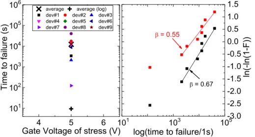
In order to evaluate the degradation mechanism responsible of the catastrophic failure, we stressed 9 devices with 70 nm channel width at constant voltage (VGS= 5 V) until failure (Fig. 5(left)). The
degrada-tion trend of the gate current shows an abrupt increase of the gate current. When the gate current reaches the value of 10−4A the devices fail. Failure is ascribed to a time-dependent defect generation/perco-lation through the oxide. The corresponding Weibull plot is reported in (Fig. 5(right)), and demonstrates a shape parameter (β) equal to 0.55 for the Weibull distribution calculated at 99% of confidence level and 0.67 at 50% of confidence level. Such low values of the shape para-meterβ (< 1) indicate that, for the analyzed devices with 15 nm di-electric, the failure rate decreases with time; this is typical for extrinsic failure mechanisms in good agreement with the hypothesis of dielectric breakdown [10].
We stressed at the same gate voltage (5 V) 8 devices with 280 nm channel width until failure, the comparison of the Weibull plots is re-ported inFig. 6. The devices with wider channel show higher robust-ness.
To formulate a hypothesis on the physical location of degradation, we carried out 2D simulations. InFig. 7we report the simulated electric field at VGS= 5 V: we show the comparison between two devices with
different fin width 70 nm (Fig. 7(a)), 195 nm (Fig. 7(b)) and 280 nm (Fig. 7(c)). The peak of the electricfield is located at the corner of the dielectric independently from the channel length. The value of the si-mulated peak of electricfield is higher than Al2O3dielectric breakdown
reported in literature (8 MV/cm) [11] due to the simplified simulated
structure (in the real device thefin corners are not exactly 90° corners and the actual thickness of the dielectric at the edge is not taken into account). It is worth noticing that the value of the electricfield when the device is submitted to 5 V of gate voltage of stress is higher for the
Fig. 5. (left) Constant voltage stress performed with VGstress= 5 V and VD= VS= 0 V performed for 9 devices, (right). Weibull plot at 50% confidence level (black curve) and at 99% (red curve). (For interpretation of the references to colour in thisfigure legend, the reader is referred to the web version of this article.)
Fig. 6. Comparison of the Weibull plots at 99% of confidence level for devices with 70 nm channel (black curve) and 280 nm channel (red curve). (For in-terpretation of the references to colour in thisfigure legend, the reader is re-ferred to the web version of this article.)
M. Ruzzarin et al. Microelectronics Reliability 88–90 (2018) 620–626
device with shorter GaNfin width (70 nm) (Fig. 8). Failure is supposed to take place in correspondence of the gate edge, where the electric field is maximum.
3.2. High drain voltage in OFF-state
Fig. 9(a) reports the results of a step stress test performed by
applying a constant voltage stress with VG= VS= 0 V and by
in-creasing the drain voltage of 20 V every 120 s.
For VDstress< 180 V, gate current increases slightly at each step of
stress; also, an increase in the noise superimposed to drain leakage is observed during stress time. At VDstress= 200 V, the gate current
in-creases of 4 orders of magnitude, indicating a substantial failure of the device. The catastrophic failure (determined when the drain current
Fig. 7. Simulation of the electricfield within the device when the stress voltage is 5 V. The electric field shows the maximum at the insulator corner and it is higher for device with 70 nm channel (a) than the 195 nm channel (b) and 280 nm channel (c).
reaches 8 mA) occurs at VDstress= 280 V.
In order to evaluate the time-dependence of the degradation pro-cess, we stressed one device with constant voltage stress up to failure (Fig. 9). The stress experiment was carried out at 280 V. In this case the device shows a constant gate current at the beginning of stress (possible kinetics related to trapping in the oxide might be faster than the sam-pling rate at the high adopted voltage). After few seconds of stress, the noise superimposed to gate leakage starts increasing, demonstrating the generation of defects within the dielectric. Random conduction through such defects results in a noisy current [6]. A catastrophic failure is reached after 2 h of stress, and consists in an abrupt increase in the gate leakage current. InFig. 10the simulation of the electricfield within two devices with different GaN channel length (70 nm (Fig. 10(a)) and 195 nm (Fig. 10(b))) submitted to high drain bias (VD= 50 V,
VG= VS= 0 V).
The devices show the peak of the electricfield (3 · 106V cm−1) at
the corner of the dielectric. However, the maximum value of electric field in the drift layer under the GaN channel is 5 · 105
V cm−1for the 70 nm-channel and 1 · 105V cm−1for the device with channel length of
195 nm. On the basis of experimental evidences and simulations, we can conclude that the failure of the device is due to a time-dependent dielectric breakdown and devices with wider GaN channel show a stronger robustness.
4. Conclusions
This paper reports an extensive analysis of the degradation current trends and mechanisms on GaN-on-GaN vertical FETs. This recent technology is very promising but little is known about the stability of these devices under positive gate bias and under high drain bias in OFF state. By means of step stress analysis, constant voltage stress and si-mulations we demonstrate:
(i) during step-stress tests at positive gate bias, GaN VFETs show an increase in gate leakage (creation of defects in the oxide), a positive shift of the threshold voltage (injection of electrons from channel to oxide), and a catastrophic failure for VGS> 5.5 V. Degradation is
ascribed to the creation of percolation paths and to the breakdown of the gate dielectric. 2D simulations permit to locate the failure point at the edge of the gate, within the dielectric.
(ii) When submitted to drain bias in OFF-state, the devices show a catastrophic failure for voltages higher than VDstress> 280 V.
Failure is ascribed to the time-dependent breakdown of the gate dielectric, at the gate edge. The results of simulations and experi-mental analyses suggest that a stronger reliability can be reached through the widening of the current channel.
Acknowledgements
The devices studied in this paper were fabricated thanks to the partial support of the ARPA-E Switches program, monitored by Dr. Isik Kizilyalli. This research activity was partly funded by project“Novel vertical GaN-devices for next generation power conversion”, NoveGaN (University of Padova), through the STARS CoG Grants call.
Fig. 8. Simulation of the electricfield when the device is submitted to 5 V for two GaN channel lengths (70 nm, 195 nm and 280 nm). The electricfield is simulated along the cut at y = 6.51μm reported in the inset figure.
0
300
600
900
1200
1500
1800
10
-710
-610
-510
-410
-310
-210
-110
010
110
2Gate Current (A/cm
2
)
Time (s)
0
40
80
120
160
200
240
280
Drain Volta
ge (V)
20V/step, 120s each step VG =VS = VB=0 V Catastrophic failure VDst = 280 V 10-4 10-3 10-2 10-1 100 10-9 10-8 10-7 10-6 10-5 10-4 10-3 10-2 10-1 100 101 102
Gate Current (A/cm
2)
time (h)
V
Dstress=300V
a)
b)
Fig. 9. Step stress performed with VGstress= VSstress= 0 V and by increasing the VDstressby 20 V each 120 s (a). Constant voltage stress (b) with VDstress= 300 V. The device reaches the failure after 2 h of stress.
M. Ruzzarin et al. Microelectronics Reliability 88–90 (2018) 620–626
References
[1] H. Amano, Y. Baines, E. Beam, M. Borga, T. Bouchet, P.R. Chalker, M. Charles,
K. Chen, J.N. Chowdhury, R. Chu, C. De Santi, M.M. De Souza, S. Decoutere, L. Di Cioccio, B. Eckardt, T. Egawa, P. Fay, J.J. Freedsman, L. Guido, O. Häberlen, G. Haynes, T. Heckel, D. Hemakumara, P. Houston, J. Hu, M. Hua, Q. Huang, A. Huang, S. Jiang, H. Kawai, D. Kinzer, M. Kuball, A. Kumar, K.B. Lee, X. Li, D. Marcon, M. März, R. McCarthy, G. Meneghesso, M. Meneghini, E. Morvan, A. Nakajima, E.M.S. Narayanan, S. Oliver, T. Palacios, D. Piedra, M. Plissonnier, R. Reddy, M. Sun, I. Thayne, A. Torres, N. Trivellin, V. Unni, M.J. Uren, M. Van Hove, D.J. Wallis, J. Wang, J. Xie, S. Yagi, S. Yang, C. Youtsey, R. Yu, E. Zanoni, S. Zeltner, Y. Zhang, The 2018 GaN power electronics roadmap, J. Phys. D. Appl.
Phys. 51 (February) (2018) 163001.
[2] M. Meneghini, G. Meneghesso, E. Zanoni, Power GaN Devices: Materials,
Applications and Reliability, (2016).
[3] S. Chowdhury, B.L. Swenson, M.H. Wong, U.K. Mishra, Current status and scope of gallium nitride-based vertical transistors for high-power electronics application, Semicond. Sci. Technol. 28 (7) (2013) 074014, ,
https://doi.org/10.1088/0268-1242/28/7/074014.
[4] H. Otake, K. Chikamatsu, A. Yamaguchi, T. Fujishima, H. Ohta, Vertical GaN-based trench gate metal oxide semiconductorfield-effect transistors on GaN bulk sub-strates, Appl. Phys. Express 1 (1) (2008),https://doi.org/10.1143/APEX.1.011105.
[5] Y. Zhang, M. Sun, D. Piedra, J. Hu, Z. Liu, Y. Lin, X. Gao, K. Shepard, T. Palacios,
1200 V GaN verticalfin power field-effect transistors, IEEE Int. Electron Devices
Meet. (2017) 215–218.
[6] T. Uesugi, T. Kachi, Which are the future GaN power devices for automotive
ap-plications, lateral structures or vertical structures? The International Conference on Compound Semiconductor Manufacturing Technology, 2011 Which are the Future
G, 1 2011, pp. 307–310.
[7] M. Sun, Y. Zhang, X. Gao, T. Palacios, High-performance GaN verticalfin power transistors on bulk GaN substrates, IEEE Electron Device Lett. 38 (4) (2017) 509–512,https://doi.org/10.1109/LED.2017.2670925.
[8] M. Ruzzarin, M. Meneghini, D. Bisi, M. Sun, T. Palacios, G. Meneghesso, E. Zanoni, Instability of dynamic-RON and threshold voltage in GaN-on-GaN vertical field-effect transistors, IEEE Trans. Electron Devices 64 (8) (Aug. 2017) 3126–3131,
https://doi.org/10.1109/TED.2017.2716982.
[9] M. Ruzzarin, M. Meneghini, C. De Santi, G. Meneghesso, E. Zanoni, M. Sun,
T. Palacios, Degradation of vertical GaN FETs under gate and drain stress, IEEE
International Reliability Physics Symposium Proceedings, vol. 2018–March, 2018.
[10] R. Degraeve, B. Kaczer, G. Groeseneken, Degradation and breakdown in thin oxide layers: mechanisms, models and reliability prediction, Microelectron. Reliab. 39 (10) (Oct. 1999) 1445–1460,https://doi.org/10.1016/S0026-2714(99)00051-7. [11] P. Ericsson, S. Bengtsson, J. Skarp, Properties of Al203-films deposited on silicon by
atomic layer epitaxy, Microelectron. Eng. 36 (1997) 91–94,https://doi.org/10.
1016/S0167-9317(97)00022-1.