Designing an Ultra Low Quiescent Current Buck Switching
Regulator
MSSACHUSETS INSTUTEb
OF TECHNOLOGYbyI
John Underhill Gardner
NOV 13
2008
S.B. EE, M.I.T., 2007
LIBRARIES
Submitted to the Department of Electrical Engineering and Computer Science in Partial Fulfillment of the Requirements for the Degree of
Master of Engineering in Electrical Engineering and Computer Science
at the MASSACHUSETTS INSTITUTE OF TECHNOLOGY May 2008
@2008
Massachusetts Institute of Technology.All rights reserved.
A uthor ... ... .
Department of Electrical Engineering and Computer Science
May 9, 2008
Certified by... ...
Leon -i Shtargot
Design Engineer, Linear Technology VI-A Thesis Supervisor
Certified by... ... David J. Perreault Associate Professor M T. Tfis Supervisor Accepted by ... Arthur C. Smith Professor of Electrical Engineering Chairman, Department Committee on Graduate Theses
Designing an Ultra Low Quiescent Current Buck Switching Regulator
by
John Underhill Gardner
Submitted to the
Department of Electrical Engineering and Computer Science May 9, 2008
In Partial Fulfillment of the Requirements for the Degree of Master of Engineering in Electrical Engineering and Computer Science
Abstract
The new buck regulator proposed in this thesis was designed to operate with only a few micro-amps of supply current during no load output conditions, while maintaining low output voltage ripple. The regulator also has high efficiency for current loads above an amp to make the converter useful in a variety of applications. The specifications will be achieved
by implementing a control scheme similar to the one used in the LT3481 buck regulator.
The converter will use burst mode, pulse frequency modulation, and pulse width modulation to achieve control over the entire load range. The capabilities of a full BiCMOS process technology will be taken advantage of to enable implementation of good control dynamics at low currents. This micropower buck regulator was designed, fabricated, and tested in silicon to measure its characteristics as compared to simulation and desired specifications.
VI-A Thesis Supervisor: Leonard Shtargot Title: Design Engineer, Linear Technology
Thesis Supervisor: David J. Perreault Title: Associate Professor
Acknowledgments
Many people were integral to the completion of this thesis. I would like to acknowledge Linear Technology Corporation for providing me the opportunity to work on this thesis project. I am particularly thankful to have worked with Leonard Shtargot as my Linear thesis supervisor. He was always there to answer my numerous questions and provide his technical expertise. His excitement and passion for analog circuit design has been inspiring. I am also appreciative of the help of several other Linear Engineers, namely Jeff Witt, John Tilly, John Readdie, Umair Daud, and Rich Philpott.
I would like to thank Prof. David Perreault, my faculty thesis supervisor, for his help getting me started on this project, as well as his review and comments on my work. Mike Whitaker first introduced me to Linear and has continued to lend me his experience as I progressed through the VI-A program. He has been an amazing help.
A special thanks to my roommates Kurt and Alex, as well as my friends at Linear. You
have made my transition to San Jose and the real world, a smooth and enjoyable one. I am very appreciative of my parents, Jan and John, who have always supported me throughout this project and my life. They were continually interested and inquisitive about my work. Bless their hearts for a lifetime of caring and love.
I must also mention Nick Diaz who started me on my current academic path. His mentorship, starting when I was only ten, sparked my love for math and science, and taught me the fun of pursuing my academic dreams. His impact on my life has been a blessing.
Contents
1 Introduction 19 1.1 Micropower . . . . 20 1.2 Prior Work . . . . 20 1.3 Proposed Work . . . . 22 1.4 Applications . . . . 22 1.5 Batteries . . . . 23 1.6 Thesis Overview . . . . 25 2 System Overview 27 2.1 Buck Switching Regulator . . . . 272.2 Control Scheme . . . . 28
2.2.1 Pulse Width Modulation . . . . 29
2.2.2 Burst Mode and Pulse Frequency Modulation . . . . 31
2.3 Optimizing the Circuit for Ultralow Quiescent Current . . . . 32
3 Low Power Circuits 35 3.1 Device Capacitance . . . . 35
3.2 Subthreshold Operation . . . . 39
3.3 Base Currents and Saturation . . . . 42
3.4 Leakage . . . . 43
4 Control Loop Modeling for Frequency Compensation 47 4.1 Voltage Mode Model . . . . 47
4.2 Current Mode Model . . . . 49
4.4 Phase Lead Capacitance . 5 Chip Design 5.1 Circuits . . . . 5.1.1 Bandgap . . . . 5.1.2 Error Amplifier . . . . 5.1.3 PG Comparator . . . . 5.1.4 Burst Logic . . . . 5.1.5 Regulator Buffer . . . . 5.1.6 Startup Circuit . . . . 5.1.7 Shutdown Circuit . . . . 5.1.8 Current Limit . . . .
5.1.9 High Power Interfacing . . . . .
5.1.10 Internal Options . . . . 5.2 Layout . . . . 5.2.1 Bandgap Layout . . . .
5.2.2 Coupling Effects . . . .
5.2.3 Matching . . . .
5.3 Total Quiescent Current Consumption
6 Measured Data
6.1 Test Setup . . . .
6.2 Quiescent Current . . . . 6.3 Current Limit and Minimum Input
6.4 Low Output Ripple . . . .
6.5 Double Pulsing . . . . 6.6 Bandgap . . . .
6.7 Error Amplifier . . . . 6.8 Frequency and Transient Response
Voltage
6.9 Efficiency
7 Conclusion
A Vbe Temperature Dependence
. . . . 10 7 111 113 . . . . 56 59 . . . . 59 . . . . 60 . . . . 65 . . . . 68 . . . . 70 . . . . 71 . . . . 72 . . . . 75 . . . . 76 . . . . 77 . . . . 78 . . . . 79 . . . . 79 . . . . 80 . . . . 81 . . . . 83 85 . . . . 85 . . . . 89 . . . . 94 . . . . 96 . . . . 98 . . . . 99 . . . . 101 . . . . 103
List of Figures
1-1 Generalized Supply Current vs. Load Current curve for a micropower and a
non-micropower converter. . . . . 20
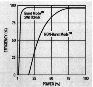
1-2 Increased efficiency of a micropower part at low output current loads. [3] (Used with permission) . . . . 21
1-3 Example System Utilizing Energy Harvesting . . . . 23
2-1 Basic Buck Switching Regulator Topology . . . . 27
2-2 Typical Application Circuit for Proposed Part . . . . 28
2-3 Block Diagram for LT3481 Buck Converter showing internal control scheme, as well as external component connections.[10] (Used with permission) . . . 29
2-4 LT3481 Full Frequency Continuous Mode Operation[10] (Used with permission) 31 2-5 LT3481 Burst Mode Switching Waveforms[10] (Used with permission) . . . 32
2-6 (A) Transition between Burst Mode and PWM when the sleep timer is slower than the programmed switching frequency. (B) Transition between Burst Mode and PWM when the sleep timer is faster than the programmed switch-ing frequency . . . . 34
3-1 NPN and PNP Structures . . . . 36
3-2 NMOS and PMOS Structures . . . . 37
3-3 Comparison of slew rates for a MOS and bipolar transistor each loaded by a 100nA current mirror. . . . . 38
3-4 Transconductance versus current for NPN and NMOS devices. When the MOS devices are in subthreshold their transconductance is proportional to current, as are the NPN devices. . . . . 41
3-5 Intrinsic gain (gmro) versus current for NPN devices with different epi
dop-ings and NMOS devices with different gate lengths. When the MOS are in subthreshold threshold their intrinsic gain is maximized and independent of current. . . . . 42
3-6 Simulated leakage current plotted against T3e- , the theoretical
tempera-ture dependence. ... ... 44
4-1 Basic circuit for a buck switching regulator. . . . . 47 4-2 Basic average circuit model for a buck switching regulator. The NPN switch
has been replaced with a current source of value diL and the diode has been replaced with a voltage source of value dvIN . . . . . .. . . . . -..
48
4-3 Block diagram of the current mode control loop. The inherent buck converter system regulates an output based on the duty cycle of the switch. The feedback through the error amplifier generates a control voltage, which sets the peak current control signal. The peak current control signal determines the duty cycle; thus the control voltage only indirectly sets the duty cycle. . 49 4-4 The inductor current over one switching period. Geometry is used to find
the average inductor current as a function of the peak inductor current. . . 50
4-5 Bode plot showing the desired poles and zeros in the loop transfer function after proper compensation. . . . . 53
4-6 Diagram showing how the compensation scheme is achieved and modeled with a schem atic. . . . . 54 4-7 Bode plot showing the poles and zeros in the loop transfer function. . . . . 56
5-1 Block Diagram for LT3480 Buck Converter. The blocks which remain pow-ered on during burst mode are circled.[11] (Used with permission) . . . . . 60 5-2 Block Diagram of the Brokaw bandgap circuit . . . . 61 5-3 Block diagram of control loop with error amplifier circuit explicitly included.
This diagram is used to simulate frequency and transient response of regulator. 67 5-4 Bode Plot of the compensated control loop. The crossover frequency of
43.2kHz with 69.7 degrees phase margin is labeled. . . . . 68 5-5 Bode Plot of the compensated control loop. The crossover frequency of
5-6 Block diagram for PG comparator circuit . . . . 69 5-7 Block diagram of buffer between micropower and power internal rails. . . . 71 5-8 Two self biasing circuits . . . . 73 5-9 Example startup circuits. Istart connects to the self-bias circuit and draws
current to prevent the zero current state. . . . . 73 5-10 Final startup circuit which provides current to the micropower circuitry. . . 74
5-11 Block diagram for shutdown circuit . . . . 76 5-12 Block diagram for buffering intermediate voltage references from high power
circuit base currents. . . . . 77 5-13 Layout of the two bandgap NPN transistors. Their layout is identical except
for the number of emitters. . . . . 79
5-14 Layout showing the size of VC node. Notice that QCLAMP2 and the series compensation resistor are placed close to the MOS to limit the node size. The picture also shows the metal shielding of the compensation resistor. . . 81 5-15 LT3480 quiescent current consumption. The total Iq is 98.48PA. . . . . 84
5-16 Thesis Project quiescent current consumption. The total Iq is 1.56/1A. . . . 84
6-1 Picture of the probe insert used to directly probe die on a wafer. The
switch-ing regulator circuit is built onto the board so that chips can be tested while on wafer. The copper ring is a ground ring. . . . . 86 6-2 Picture of the board layout used for testing. The packaged die is open and
unpassivated so that internal nodes can be probed and options can be accessed. 87
6-3 Picture of the fabricated part. A majority of the MOS devices can be seen
in the clump of traces near the lower right corner of the die. . . . . 88
6-4 The quiescent current measured during switching for a range of input volt-ages. The feedback resistor divider remained in a ratio of 1:1.7, but for each curve the smaller resistor was either 1O0kQ, 1MSI, or 10MZ. As shown, the quiescent current decreases for larger feedback resistor values. . . . . 91 6-5 The quiescent current is shown to increase with temperature. The increase
is exponential, which seems to indicate it is caused by diode leakage. . . .. 93 6-6 The current limit plotted against duty cycle for both 3.3V and 5V outputs. 94
6-7 The maximum load current plotted against the input voltage while regulating
a 3.3V or 5V output. . . . . 95 6-8 The minimum input voltage across load to maintain a regulated 3.38V or
4.84V output. . . . . 96 6-9 Switch voltage (top trace), inductor current (middle trace), and output
rip-ple (lower trace) for four different output loads. Even though the four os-cilloscope shots show the converter operating in different modes, the output voltage ripple is always less than 10mV. The output capacitor was 22pF in all cases. . . . . 97 6-10 The voltage on the RT pin (top trace) and the inductor current (lower trace)
for a long sleep timer with double pulsing and a short sleep timer with single pulsing. . . . . 98 6-11 The feedback pin (or bandgap voltage) measured over temperature for a
trimmed bandgap reference operating with 100nA per leg. For the tempera-ture range typically specified for ICs (-55'C to 1251C) the voltage varies by less than 4m V. . . . . 100 6-12 The feedback pin (or bandgap voltage) measured over temperature for an
untrimmed bandgap reference operating with 50nA per leg. The reference continues to work properly at high and low temperatures, despite operating at low currents. These curve indicates that the reference voltage should vary
by less than 5mV once trimmed. . . . . 101 6-13 Measured error amplifier output current when Vc is fixed at
1V.
. . . . 102 6-14 Measured transconductance of error amplifier. . . . . 1026-15 Response to a 0.5A to
1A
and then a 1A to 0.5A step in the output load. The upper trace is the output voltage of the regulator and shows a 50mV peak overshoot in response to the load step. The lower trace is the inductor current where the 10mV per division corresponds to 500mA per division. . 106 6-16 The measured bode plot with Cc = 4pF, RC = 3Mg, Cmt = 30pF for thecase when no phase lead capacitor is used and the case when a 100pF phase lead capacitor is used. . . . . . .. . .. 107 6-17 Measured efficiency for conversion from 5V, 12V, and 24V to 3.3V over a
6-18 Measured efficiency for conversion from 12V and 24V to 5V over a load range
from 1pA to 1A . . . . 109 6-19 12V to 3.3V efficiency for use with internal feedback resistors or a shorter
sleep timer as compared to the efficiency without these options. The use of internal feedback resistors increases the efficiency by one to three percent for loads below 100pA, while the use of a shorter sleep timer increases the efficiency by about six percent for loads between 100pA and 10mA. Note that the shorter sleep timer curve uses external 1 MQ and 1.7 MQ feedback resistors and internal feedback resistor curve used the standard sleep timer length. . . . . 110
B-1 (A) PMOS current mirror analyzed for matching. (B) PMOS current mirror with source degeneration analyzed for matching. . . . . 115
List of Tables
1.1 Specifications for several current Linear Technology Buck Regulators com-pared to the proposed buck regulator specifications. [1] . . . . 21 1.2 Self discharge of several different battery chemistries at room temperature. [2] [4] 24
3.1 NPN and PNP junction capacitances for two different values of epi-doping.
These capacitances are the values with zero volts of applied DC junction bias
(C io) . . . . . 36 3.2 NMOS and PMOS device capacitances for minimum sized devices, 4pm wide
and 2im long. These capacitances are the values with zero volts of applied
DC bias... ... 37
6.1 Measurements of the current consumption of some of the main circuit blocks as compared to simulated values. . . . . 89 6.2 Reverse leakage currents for several different current and voltage diodes. . . 91 6.3 Characteristics of current pulses for different input voltages. . . . . 92
6.4 Frequency and transient response characteristics for different compensation settings. The crossover frequency and phase margin were measured directly with a machine, while the peak overshoot and time to settle back to regulation for the load steps were recorded manually based on captured oscilloscope traces. 104
Chapter 1
Introduction
There are many applications which require step-down DC-DC conversion in the milli-watt to several watt range. Among these applications are portable electronic systems, automo-tive applications, and wall transformer regulators. Battery life is a critical component for portable systems and automotive applications, thus power management must be as efficient as possible. In particular, efficiency over a range of loads can become critical. If a portable system is powered on, but the functionality requiring the regulated DC voltage is not be-ing used, the efficiency of the converter can significantly decrease. A specific example is modern CMOS memory and microcontrollers, which need a DC bias to hold state, but do not consume appreciable current. In such cases, efficiently plummets when no current is being drawn from the output of the converter because all the power used by the converter to regulate the unused output voltage is wasted. This supply current can often be in the milliamp range. Therefore, there is a need to decrease the supply current necessary to op-erate the converter as the output current decreases. This has lead to the creation of a series of micropower switching regulator parts which only require ten to hundreds of micro-amps of current to operate during no load conditions. The aim of this thesis is to describe the design of a buck switching regulator circuit which only consumes a few micro-amps with disconnected load.
The Linear Technology Corporation presently sells several micropower products. The thesis work proposed here is done through Linear Technology taking advantage of the work they have done designing and fabricating micropower products. This thesis is supported by Linear Technology through the VI-A program.
1.1
Micropower
It is important to understand how a micropower regulator is different than a non-micropower regulator. Many switching regulators will require a substantial static component of supply current regardless of the output load. However, micropower regulators refer to converters which require less supply current when operating at lower output loads as shown in Fig. 1-1.
Isupply
mA Non-pPower
puA pPower
pA mA 00 'oad
Figure 1-1: Generalized Supply Current vs. Load Current curve for a micropower and a non-micropower converter.
The efficiency of a power converter is defined as the output power divided by the input power. When milli-amps of supply current are used to generate micro-amps of output current, the input power is much larger than the output power resulting in poor efficiency. However, when the supply current is comparable to the output current at small output current levels, the input and output powers are comparable, which results in significantly higher efficiency. The higher efficiencies realized by micropower parts operating at a small percentage of their total output power is depicted in Fig. 1-2.
The efficiency advantage of micropower parts is most pronounced when there is no output load, in other words when the regulated voltage is not being used. The converter supply current during conditions of no output load is referred to as quiescent current. The quiescent current is one of the primary quantities used to characterize micropower parts.
1.2
Prior Work
The efficiency advantages of micropower parts are only part of the story. Achieving low quiescent current is difficult because there are trade-offs which often have to be made. Many
Figure 1-2: Increased efficiency of a micropower part at low output current loads. [3] (Used with permission)
control schemes are such that output voltage ripple is quite large in micropower operation when compared to full frequency operation, independent of the output capacitance. Users can tolerate ripple voltage of ten or twenty milli-volts, but larger amounts of output ripple become unacceptable. Also, typically the maximum load current the regulator is able to provide is smaller when micropower operation is incorporated because control and stability of the converter becomes difficult when the load range spans several orders of magnitude.
The trade offs in designing micropower buck parts can be seen by examining a list of several Linear Technology micropower buck regulators shown in Table 1. The parts which can supply the highest amount of output current also have the largest quiescent current
(LT1977 and LT3435). The converse is also true; the parts with low quiescent current also
have low maximum output current (LT1934 and LT3470).
Part Vin,max (V) Iout,max(A) ,,,pply (pA) Burst Vut Ripple (mV)
LT1934 34 0.3 12 40 LT1977 60 1.24 100 40 LT3435 60 2.4 100 80 LT3437 80 0.4 75 20 LT3470 40 0.2 25 20 LT3481 36 2 50 10 Proposed 36 2 1-10 10
Table 1.1: Specifications for several current Linear Technology Buck Regulators compared to the proposed buck regulator specifications. [1]
The output ripple in burst mode is listed. This specification is difficult to cite because it depends on the exact current load and the type/size of the output capacitor used. The values listed in the table correspond the the peak-to-peak values in switching waveform plots contained in the part data sheets. It is hard to make a comparison between them, but it is clear that more than twenty or thirty milli-volts is quite common.
1.3
Proposed Work
The new proposed buck regulator has very aggressive specifications, as listed in Table 1.1. It builds upon the LT3481, which has better performance than the other parts listed. The LT3481 has increased output load range with low current ripple, while maintaining low supply current. However, a part with these qualities, but even lower quiescent current is very desirable. The LT1934 was very popular and sold in the millions because of its very low quiescent current, even though it has undesirable voltage ripple and non-fixed frequency control. Therefore, the proposed part will be of interest to many customers with many different applications.
1.4
Applications
There is little reason to redesign a regulator without considering whether there will be need for new features and more impressive design specifications. A buck regulator with a quiescent current of only a few micro-amps does have several interesting applications.
The first of these applications are systems where the regulated voltage is necessary, but current is not always being drawn from the output. For example, modern CMOS memory and microcontrollers need a regulated voltage and almost no current when remembering or holding a certain state, but when switching state will require more power. The user does not want the regulator to drain the battery unnecessarily and would like good efficiency during idle states, so a low quiescent current regulator would be desirable. This is especially true in laptops and other portable applications where battery life is a big issue and every little bit of efficiency counts.
The second set of applications are systems where the product is not being used a vast majority of the time and the battery cannot be discharged during this time period. One specific example of this kind of system is a fire alarm. A majority of the time it is simply
waiting to detect a situation where it needs to respond and start fully operating. An ultra low quiescent current regulator would be good in this scenario because the battery needs to survive reliably for a long time in such a product without being depleted by the converter when idling with no load.
The third set of applications are energy harvesting systems. Energy harvesters collect energy from the environment in the form of vibrations, light, or thermal gradients. The difficulty with these systems is that only small amounts of energy can be collected and the energy does not come in a constant form. Therefore, an energy storage system has to be set up like the one in Fig. 1-3.
Charger Buck
Energy + Load
Harvester -Battery
Figure 1-3: Example System Utilizing Energy Harvesting
The voltage from energy harvesters is usually too low to store and needs to be interfaced with a charger or boost converter to charge a battery or similar energy storage device. Then the stored energy needs to be regulated before it can be used to power a load device. Since the energy harvester is only able to gather small amounts of power into the battery, the system is only capable of operating loads with small power requirements. Therefore, the regulator used to source the load needs to be efficient at light loads to make the system viable. The ultra low quiescent current regulator described in this thesis is such a candidate.
1.5
Batteries
While discussing the effect the converter will have on draining the battery, one also has to consider the natural self-discharge of the battery. Batteries have a finite shelf-life as their charge is slowly drained over time. The self-discharge of a battery depends on battery chemistry, temperature, and whether the battery is a primary or a secondary (rechargeable) battery.
Nickel Metal Hydride (NiMH) are the worst with 15% to 20% and 30% per month, respec-tively. Lead acid and lithium chemistries are better with lead acid discharging 4% to 6% of their charge per month and lithium secondary battery discharge being half that of lead acid batteries. Primary batteries are significantly better than rechargable batteries in terms of self-discharge. Alkalines can have shelf-lives of around 5 years, while lithium primaries can have 10 to 15 year shelf-lives.[12]
Battery Chemistry Voltage Capacity Self-Discharge Rate Leakage Panasonic
LC-R122R2P Lead-Acid 12V 2.2Ah 5yrs 50.2pA
Panasonic
6AM-6PI Alkaline 9V 500mAh 5yrs to 85% 1.7pA
Energizer NH22 NiMH 9V 175mAh 21days to 70% 104.2pA
Energizer X22 Alkaline 9V 655mAh 5yrs to 80% 3.0pA
Energizer L91 Lithium 1.2V 3000mAh 15yrs to 90% 2.3pLA
Table 1.2: Self discharge of several different battery chemistries at room temperature. [2] [4]
The self-discharge characteristics of several specific batteries are shown as examples of self-discharge for different battery chemistries in Table 1.2. The superior performance of primary alkaline and lithium batteries to secondary lead-acid and NiMH batteries is clear. It is important to note that battery discharge is specified as a percentage of total capacity. Therefore, batteries with larger current capacities will have more leakage even for the same battery type. This means that NiMH are even worse, while lead-acid and lithium are better when comparing them based on leakage per Ah, than just leakage current. All the values listed in the table are for room temp (25"C). The self-discharge will approximately double for every additional 10'C of temperature.
When using a primary 9V battery, as might be used in a fire alarm application, there are only two to three micro-amps of self-discharge current. This is comparable to the quiescent current of the proposed buck converter. If the quiescent current were larger, as in presently available regulators, the converter itself would be the limiting factor in battery lifetime. However, if the target quiescent current of the proposed converter was significantly lower than a few micro-amps, there would be diminished increase in battery life because the battery self discharge would be the limiting factor. Therefore, the chosen quiescent current goal of one to ten micro-amps for the project is a good one.
lithium-ion batteries in laptops, lowering the quiescent current of the regulator below the self-discharge rate of the battery can be desirable. Minimizing the converter quiescent current still improves battery life, even if the battery self-discharge is greater than the quiescent current, one just observes diminishing returns because the battery self-discharge rate is limiting the battery life, not the converter. However, perhaps the most important aspect of a low quiescent current regulator is that the user does not have to worry about the power consumption of the converter during no load conditions because the quiescent current is much lower than the battery self-discharge rate.
1.6
Thesis Overview
Chapter 2 will cover the basics of the buck switching regulator operation and control. Then, the merits of low current circuits will be described in relation to the project in Chapter 3. Chapter 4 will examine the modeling of the control loop, so that a compensation network can be devised. Next, the design of each low current sub-circuit of the regulator will be detailed in Chapter 5. Chapter 6 will review the results of the bench tested silicon. Finally, the issues discussed in the thesis will be summarized in Chapter 7.
Chapter 2
System Overview
This chapter describes the basics of buck switching regulators and buck switching regula-tor integrated circuits. It then outlines the control scheme used in the proposed project, including how burst mode is used to achieve micropower operation.
2.1
Buck Switching Regulator
The circuit topology of a basic buck switching regulator is shown in Fig. 2-1.
Vin+ C R
Figure 2-1: Basic Buck Switching Regulator Topology
This circuit does not show any of the feedback circuitry which is used to control and drive the switch. The feedback circuitry and the choice of switch are two of the most difficult parts of designing a buck regulator system. The switch and the feedback circuitry are the aspects of the regulator which are integrated in the proposed IC, and the other elements are discrete, external components.
The typical application circuit for the proposed part is shown in Fig. 2-2. The internal switch is connected between the Via and SW pins. The diode D1, inductor L1, and capacitors
Coat and Cim are the same as shown in the basic topology. The resistors R1 and R2 form a divider which measures the output voltage and inputs it to the feedback pin FB. The other
BD RPg
VIN Vin BOOST 150k -VOUT
Cboost -SHDN 0.47PF LI Gin --- RT4.7pH R2 4.7pF
tRT
T D F 1.72Meg Cout GND FE 60k RI 22pF 1 MegFigure 2-2: Typical Application Circuit for Proposed Part
external components help implement useful features of the IC. The shutdown pin (SHDN) can be tied low to stop the part from switching and is connected high, usually to Vi, for normal operation. A resistor is connected to the RT pin to program the switching frequency of part to be anywhere from 200kHz to 2.4MHz. A capacitor is connected to the BOOST pin, which is used to generate a voltage higher than V, which is needed to more efficiently drive the internal switch. Finally, the resistor connected to the PG, or Power Good, pin acts as a pull up resistor and the output of the PG pin goes high when Vt comes within
10% of its regulated value.
2.2
Control Scheme
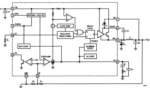
Now that the basic system has been outlined, the operation of the control scheme will be explained. The primary job of the IC is to properly control the internal switch. The control scheme for the new buck IC is the same as the control scheme used in the LT3481 buck converter. The LT3481 is a recently designed buck converter, which has low quiescent current, low output ripple voltage, and a large range of current loads, while maintaining good efficiency. The block diagram for the LT3481 is shown in Fig. 2-3.
-- 3
JR
5 IAS INIERNAI I W SOP.SSREF 00S
5
~
SOPECOP LWTCH 2OSFigure 2-3: Block Diagram for LT3481 Buck Converter showing internal control scheme, as well as external component connections. [101 (Used with permission)
through the FB pin using an external resistor voltage divider. The voltage on the FB pin is compared to an internal reference voltage using an error transconductance amplifier. The voltage error signal is one input to the internal control system. Since the controller is trying to reduce the voltage error to zero, the resistor divider ratio is used to set the desired output voltage of the converter.
The switch current is measured by the resistor between the Vmn pin and the collector of the
internal
power switch. This current is monitored by an amplifier and comparator, and is the second input to the internal control system. Using these two feedback signals, the output voltage for differentloads
is regulated through Pulse Width Modulation (PWM) and Pulse Frequency Modulation (PFM) or Burst Mode operation.2.2.1 Pulse Width Modulation
PWM is the dominant control method during normal operation, namely medium to large current loads. During PWM the frequency of the drive applied to the base of the power switch remains constant. However, the duty ratio, or time the switch is driven such that it is on, changes to control the buck regulator. This control scheme implements current mode control, meaning it controls both the output voltage and inductor current. In a peak current controlled converter, which we are considering, the duty ratio is established implicitly by
setting current limits. Namely, the switch is turned off when the switch current ramps to a peak current limit [20]. This leads to the generation of a particular duty ratio. The current limit is based upon the voltage error signal from the transconductance amplifier. The error signal provides a DC shift to a sawtooth slope compensator waveform, which when compared to the measured switch current, trips a comparator turning off the switch drive. When the error is large and the output voltage is low the current limit is increased, so the output capacitor can charge to the desired output voltage. Conversely, when the output voltage is too high the current limit is decreased, so the capacitor can discharge to achieve the desired output voltage. In this way, both the inductor current and output voltage are controlled by PWM. [10] The slope compensator, error amp, summing junction, comparator, and power switch driver can all be seen on the block diagram in Fig. 2-3.
In a buck topology, the average inductor current is equal to the average output current, since the inductor is always connected to the output and the'capacitor draws no average current. The average input current is equal to the average switch current, which will be zero when the switch is off and equal to the positively ramping inductor current when the switch is on. The relationship showing how duty ratio controls the input and output current and voltage ratios under ideal conditions in continuous conduction mode is summarized below.[14]
,ou i (2.1)
Vou = DV (2.2)
Even though these equations will not be exact in real converters with less than perfect efficiency, they show the general trends between duty ratio and output current and volt-age. The controller will adjust the operating point duty ratio to achieve proper DC voltage conversion. The system will be compensated such that when output transients and pertur-bations in input, output, and load conditions occur the system can quickly and accurately return the output voltage and inductor current to the desired regulated levels.
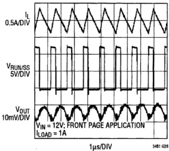
PWM control can be seen in the LT3481 switching waveforms in Fig. 2-4. The current in the inductor ramps up when the switch is on and ramps down when the switch is off.
0.5A/DIV
VRUN/SS 5V/DIV
VOUT 1 OmV/DIV
VIN 12V; FRONT PAG
APPLICATION-ILOAD =
1A
1Is/DIV UA1 G26
Figure 2-4: LT3481 Full Frequency Continuous Mode Operation10} (Used with permission)
2.2.2 Burst Mode and Pulse Frequency Modulation
Burst Mode is a part of the control scheme which takes over at low current loads. A converter can use on the order of milli-amps of supply current during normal operation. However, during light load operation, in the limit of zero load current, the supply current can contribute significant loss in efficiency. Burst mode strives to decrease the necessary supply current down to the tens of micro-amps level to increase light load efficiency. This functionality is implemented by shutting down all the control circuitry, except for the error amplifier, during light load conditions when the output voltage is high. Then, as low amounts of current from the output capacitor are supplied to the load, the output voltage will drop. When the error amplifier senses the drop in output voltage, it will turn on, or "wake-up," all the control circuitry and drive the switch, thus recharging the output capacitor and restoring the output voltage. Then, all the control circuitry will be put back to "sleep" again, namely the control circuitry will be shut off until it needs to turn on again to drive the switch.
This method for light load control is good for significantly reducing the supply current and increasing the converter efficiency. However, swings in output voltage are inherent to the process, so large amounts of output voltage ripple can result. One way to reduce the output voltage ripple is to burst frequently with small charge impulses. Therefore,
A. & j
,
& N A &
4 V V \.1 V 'V
the output capacitor will have less negative ramping time, thus reducing the peak-to-peak output voltage swing. Bursting more frequently, however, will most likely require more supply current, so a trade-off must be struck between voltage ripple and quiescent current.
VIN = 12V; FRONT PAGE APPLICATION 'LOAD lm IL 1], 0. 5AND IV 5V/DIV VOUT 10mVIDIV --
~tub
5ps/DIV M81 G24Figure 2-5: LT3481 Burst Mode Switching Waveforms[10] (Used with permission)
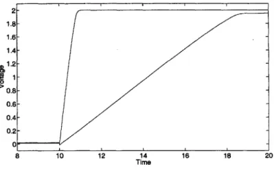
Fig. 2-5 shows the switching waveforms for the LT3481 in burst mode operation. One observes the inductor current pulses, which are used to charge the output capacitor. Also, the linearly decreasing output voltage as the output capacitor discharges can be seen. It is interesting to note that when the control circuitry "wakes up" the power switch is only turned on once. If the switch turned on multiple times the output ripple would be increased, because the output capacitor would be charged to a higher voltage and would take a longer time to discharge to the same control turn-on trip point. The output voltage ripple in this example is only 10 mV. This is the same as the ripple during normal operation in Fig. 2-4 and smaller than the burst mode ripple voltages for the other parts in Table. 1. This level of ripple voltage will be the goal of the new buck regulator.
2.3
Optimizing the Circuit for Ultralow Quiescent Current
The goal of this project is to minimize the current consumption of the circuit when in sleep mode. This means that only about a third of the circuit needs to be optimized for low power operation because the other two-thirds will be powered down. However, the
current consumption of the part while switching will necessarily be larger than the sleep current, because when all the circuitry wakes up there will be brief moments of high current consumption. Even though it is beyond the scope of this project to design the circuitry which "wakes up" to be low power, there are ways the system can be optimized so that the effects of the high power circuitry can be minimized to keep the quiescent current during switching as close as possible to the current consumption during sleep.
There are two ways in which the influence of the high power circuitry can be minimized. The first is to minimize the number of times the part has to wake-up by maximizing the period between pulses when in burst mode. The part has to pulse after the output capacitor has been sufficiently discharged. The primary discharge paths for the capacitor when there is no output load are the DC current in the feedback resistor divider and DC reverse leakage current through the catch diode. Therefore, the simple, yet important, steps of maximizing the total resistance of the feedback divider and selecting a low leakage diode will maximize the period between pulses.
The second way to minimize the influence of the high power circuitry to is minimize the total time that the high power circuitry is awake each time it turns on. This time period is controlled by a sleep timer, which keeps all the high power circuitry on after a current pulse until the timer expires and the high power circuitry is then powered down. When the high power circuitry is powered down, the part can immediately switch once the error amplifier signals the need for a current pulse. If the part went to sleep immediately after a current pulse, then the next current pulse could come very quickly and the part could end up switching faster than the programmed switching frequency.
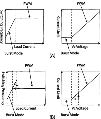
The plots in Fig. 2-6 show how the chip transitions between Burst Mode and PWM. When in burst mode, to provide increased load current the switching frequency is increased and the current limit is held constant. When in PWM mode, the switching frequency is constant and the current limit is increased to provide increased load current[21]. The sleep timer in the upper plots (Fig. 2-6 (A)) is 5ps, which corresponds to the minimum programmable switching frequency of 200kHz. Therefore, there are smooth transitions between Burst Mode and PWM. However, the lower plots (Fig. 2-6 (B)) show the result of a shorter sleep timer. When transitioning from Burst Mode to PWM, the part can burst faster than the programmed switching frequency. Therefore, there is a range of load currents where the part can regulate in either burst or PWM mode. There is hysteresis in
PWM PWM Load Current Burst Mode LflM LodCurn Burs Mod 3
(A)
IDf-(B)
PWM Vc Voltage Burst Mode PWM Vc Voltage Burst ModeFigure 2-6: (A) Transition between Burst Mode and PWM when the sleep timer is slower than the programmed switching frequency. (B) Transition between Burst Mode and PWM when the sleep timer is faster than the programmed switching frequency
the load current where the transition between modes occurs and this hysteresis increases for smaller sleep timer durations.
Small sleep timer periods may lead to instabilities in the control loop of the regulator. However, the hysteresis between mode transitions is not necessarily detrimental. Since there is considerable hysteresis, as long as the part is able to regulate around a narrow control voltage range for a given load current, then there should not be erratic transitioning between modes, even when operating in the load range where two different regulation points exist. This means that decreasing the sleep timer to help minimize the quiescent current is worth investigating.
Chapter 3
Low Power Circuits
The design work in this thesis is based around the idea of redesigning sub-circuits within the switching regulator to operate with low power consumption. The goal of a buck regulator requiring only a few micro-amps of quiescent current can only be realized if the individual sub-circuits require hundreds or even tens of nano-amps of DC current. This chapter de-scribes the general approach to designing circuits for low current operation. It focuses on the differences between bipolar and MOS devices, in terms of capacitance, gain, leakage, and transitioning between different modes of operation. Understanding the advantages and disadvantages of the devices available in the process is essential to designing circuits capable of taking advantage of the full BiCMOS process used for this thesis project.
3.1
Device Capacitance
Speed is an important characteristic of many analog circuits. Amplifiers and comparators are often speed critical and need to be fast. In switching regulators there are often nodes which need to slew over several volts quickly. Parasitic capacitances need to be charged as a node is slewing. Charging such capacitances becomes more difficult when dealing with small currents and speed can be limited by parasitic capacitances. The best way to avoid these problems when operating with small currents is to minimize the capacitance of the devices one is using or to use devices with the smallest capacitances.
The structure of an NPN and a PNP device are shown in Fig. 3-1. There are three capacitances inherent in the NPN structure. The base-to-emitter capacitance (Cje), the base-to-collector capacitance (Cjc), and the collector-to-substrate capacitance (Cjs). These
Collector Emitter Base Base Emitter Collector
ISO p Epi n ISO p Epi n ISO P
(a) NPN (b) PNP
Figure 3-1: NPN and PNP Structures
three capacitances exist in the PNP device as well, except that the PNP has a base-to-substrate rather than a collector-to-base-to-substrate capacitance. All of these capacitances are junction capacitances, which are the sum of the sidewall capacitances, which scale with the perimeter of the junction, and the vertical junction capacitance, which scales with the area of the junction. The capacitances with the substrate are more complicated because it consists of both the capacitance with the walls of the iso and the buried layer to the substrate.
NPN NPN PNP PNP
Normal Epi Light Epi Normal Epi Light Epi
Cje 16.3fF 25.5fF 16.3fF 16.3fF
Cjc 55fF 14.5fF 128fF 40.4fF
Cjs 226fF 226fF 309.9fF 309.9fF
Table 3.1: NPN and PNP junction capacitances for two different values of epi-doping. These capacitances are the values with zero volts of applied DC junction bias (Cj3 ).
The values of each of these capacitances for a few minimum sized bipolar devices in this process are listed in Table 3.1. The values listed are for zero volts of applied junction bias. For increasing bias the capacitances will decrease according to the equation C = C
1+
[7]. There are a few characteristics to notice from the table. First, the collector junction
capacitance is usually larger than the emitter junction capacitance because the collector junction is larger than the emitter junction. Second, the light epi devices have smaller collector junction capacitance. Junction capacitances are always smaller for lighter junctions because lighter junctions can deplete further. The edges of the depletion region act as plates in a parallel plate capacitor and the capacitance of such a structure is inversely proportional to the distance between the "plates". Third, the substrate junction capacitance is much
larger than the other junctions due to the significantly larger size of the junction. The
PNP device is larger than the NPN device, so sits in a larger tub having a larger substrate
capacitance.
Gate Gate
Body Source Drain Body Soure rain
ISO p l ISO p Nwell n ISO p
Epi n Epi n
(a) NMOS (b) PMOS
Figure 3-2: NMOS and PMOS Structures
The structures of NMOS and PMOS devices are shown in Fig. 3-2. The device ca-pacitances present here are the gate-to-source (C,), gate-to-drain (Cgd), source-to-body
(Cob), and drain-to-body (Cdb) capacitances. The gate-to-body capacitance exists, but it is so small that it will not be considered. The gate-to-source capacitance includes the capacitance intrinsic to charging the gate to turn on the transistor. This is the oxide capac-itance, which is inversely proportional to the oxide thickness used in the process. Overlap capacitance contributes to the gate-to-source and gate-to-drain capacitances. This is the capacitance with the drain and source regions which diffuse underneath the gate. The source and drain capacitance to the body are junction capacitances, which include sidewall and vertical junction components, just like the bipolar capacitances.
NMOS PMOS Cox 1.33 1.33 1 Cj 0.644 1 0.304 14 Am pm Cjsw 0.57 E 0.46 f Cgdo,Cgso 0.1 R 0.315 IF Cgs 7.1 fF 8.0 fF Cgd 0.4 fF 1.3 fF Csb,Cdb 17.6 fF 11.2 fF
Table 3.2: NMOS and PMOS device capacitances for minimum sized devices, 4pm wide and 2pnm long. These capacitances are the values with zero volts of applied DC bias.
The capacitances in this process for the basic NMOS and PMOS devices are listed in Table 3.2 for zero volts of applied bias. The top of the table shows the capacitances used in the transistor models, which are a function of transistor sizing. The values in the lower half of the table are capacitances between the device nodes calculated for a minimum device size of 4pm width and 2pm length.
It is easy to see that the device capacitances are much smaller for the MOS devices. Comparing the gate-to-source versus the base-to-emitter capacitances, the MOS parameters are two to three times smaller. Comparing the drain-to-gate versus the collector-to-base capacitances, the MOS parameters are more like thirty times smaller. Finally, if we assume that the body is tied to an incremental ground, the capacitance to ground is thirteen times
smaller for the NMOS drain than the NPN collector.
2 -1.8 -- 1.6- 1.4- 1.2- 0.8-- 0.6- 0.4- 0.2-0 8 10 12 14 16 18 20 Time
Figure 3-3: Comparison of slew rates for a MOS and bipolar transistor each loaded by a 100nA current mirror.
The difference between these device capacitances can be seen in a simple slew rate circuit.
A NMOS transistor, with a PMOS current mirror load attached to its drain, is turned off,
causing the NMOS drain to slew. A NPN is similarly set up with a PNP current mirror load and when the NPN is turned off, its collector will slew. This simulation was conducted with a two volt upper rail and a current mirror running 100nA of current. At any moment in time during the simulation, the output node of the bipolar transistor receives slightly more current from its load than does the MOS transistor output node from its load. Therefore, a slew rate comparison between the two devices is a fair comparison. The resulting output node voltage waveforms are shown in Fig. 3-3. The NMOS reached 90% of its final value
in 0.74ps, while the NPN reached 90% of its final value in 7.531s. The MOS circuit slews 10 times faster than the bipolar circuit. The total capacitance on the NPN collector is the NPN substrate capacitance, plus the NPN and PNP base-to-collector capacitances, which
total 409 fF. The total capacitance on the NMOS drain is the combination of the drain-to-body and drain-to-gate capacitance for both the NMOS and PMOS, which equals 30.5
fF. Therefore, based on the models, the MOS circuit is expected to be about thirteen times
faster.
3.2
Subthreshold Operation
Another important characteristic of analog circuits, including amplifiers and feedback loops, is gain [7]. Both voltage gain and current gain can be important depending on the circuit. The transconductance of both bipolar and MOS transistors will be considered. We will also consider the voltage gain of a transistor with an active load, which often occurs in basic differential-pair amplifiers. IVA BJT : m=-- ro= (3.1) Vh Ic W 1 MOS : m = 2k ID ro (3.2)
The basic equations for the transconductance and output resistance of a bipolar tran-sistor and a MOS trantran-sistor are listed in Eqn. 3.1 and 3.2, respectively. These equations hold when the the bipolar is in the forward active region where the base-to-emitter junction is forward biased and there is more than about 100 mV of collector-to-emitter bias, so that the collector-base junction is reversed biased. The MOS is in the active region where the gate-to-source voltage is above VT and the drain-to-source voltage is above about 100 mV. There is another useful region of MOS operation, which occurs at low currents. When the drain current is low, the gate-to-source voltage is nearly equal to VT or even slightly below VT. This region is called subthreshold, or alternatively referred to as weak inversion, while the normal MOS operation described above is called strong inversion. The drain current is a exponential function of Vg, (Eqn. 3.3) rather than a square-function of V, as in operation with normal current levels.
Vg a
ID = Ioe nVth (1 + AVdS) (3.3)
n = 1+ B (3.4)
Cox
The relationship between gate voltage and drain current changes because the basic mechanism behind the transistors' operation changes. Under normal operation, a channel is formed between the source and drain, and current flows due to the potential difference between the source and drain. The drain current is a drift current. In subthreshold, however, a channel does not completely form between the gate and source, and the charge flow that occurs is because of diffusion. The drain current is a diffusion current. It is no coincidence that the current equation looks similar to the current equation for a bipolar transistor, a device exhibiting current diffusion. Unlike the bipolar equation, the subthreshold current equation has an additional factor n. The voltage of the silicon between the gate and the source is less than the transistor gate voltage. It is smaller based on the capacitive divider between the oxide capacitance and the body capacitance of the device (Eqn. 3.4).
Based on the subthreshold current equation, the transconductance and output resistance can be calculated (Eqn. 3.5). The transconductance is the same as that for a bipolar except
for the factor of n. The output resistance is the same as it is in strong inversion. Empirically, the quantity lambda is the same as it is in strong inversion.
m ro = (3.5)
nVth AID
The transconductance (gm) versus current plot in Fig. 3-4 summarizes the transistor properties explained above. The MOS transistor g, is proportional to current when oper-ating is subthreshold and so has a linear curve on the plot as does the NPN transistor. At higher currents the MOS transistor comes out of subthreshold and the gm exhibits a square root of current dependence. The length of the MOS transistor has no effect on 9m when in subthreshold, but
gm
decreases with increasing length in strong inversion[9]. It is good to note that the transconductance is always greater for larger bias currents, regardless of whether it is in weak inversion or strong inversion. However, the transconductance per unit of bias current is largest when in subthreshold. Regardless of how the MOS transistor is10-- NMOS L=2pm --- NMOS L=3Rm NMOS L=4Rm NMOS L=5tm -NMOS L=1(him 10 +- N P N .... ... ... C 0 C 10 -- -cd1 -8 10~ 10- 1e 1l~ 10' 105 10~-4 Current (A)
Figure 3-4: Transconductance versus current for NPN and NMOS devices. When the MOS devices are in subthreshold their transconductance is proportional to current, as are the
NPN devices.
operated, the bipolar has larger gm for a given current consumption.
It is interesting to note that the transistor is in subthreshold for larger currents when the gate length is smaller. This makes sense because the gate voltage is smaller for a given current when the device length is smaller. For a minimum size device, the subthreshold cutoff occurs around current densities of about 250"-.
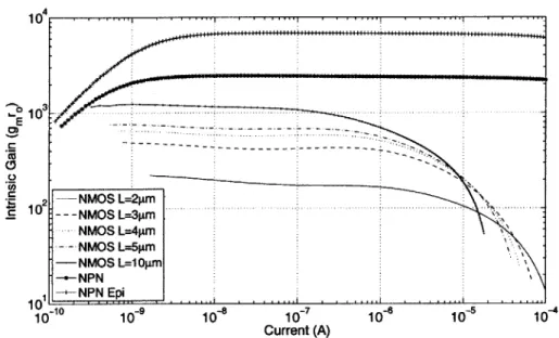
The plot of intrinsic gain (gmro) versus current in Fig. 3-5 is also instructive. The gain is independent of current when the MOS is in subthreshold because gm is proportional to current and r, is inversely proportional to current. When the MOS transistor enters strong inversion, the gain decreases because r0 is decreasing faster than gm is increasing.
The length of the transistor increases the gain when in subthreshold because the length is inversely proportional to A, which increases the output resistance for larger gate lengths[9]. The bipolar gain is flat for the majority of the plot for the same reason the MOS subthreshold gain is flat with current. The NPN with a lighter doped epi has increased gain than its higher doped counterpart, because the early voltage (VA), and thus the output resistance, is larger. At very small currents the bipolar gain falls off as the output resistance and early voltage decrease with beta degradation. As for the previous plot, the bipolar transistor gain is always larger than that of the MOS transistor for a given current consumption.
10 0 M C 10 - -- NMOS L=3pm --- M--- -=--m 1074 Current (A)
Figure 3-5: Intrinsic gain (gmro) versus current for NPN devices with different epi dopings
and NMOS devices with different gate lengths. When the MOS are in subthreshold threshold
their intrinsic gain is maximized and independent of current.
These plots show that bipolar transistors have superior small signal parameters when compared to MOS transistor operating with the same bias current. However, if one needs to use MOS transistors for their superior capacitance, speed, and size, it is advantageous to operate them in subthreshold when current is at a premium. In subthreshold, MOS tran-sistors have better intrinsic gain and gm per unit of current than when in strong inversion. Therefore, for the low current circuits being designed in this thesis, the trade off in current gain and voltage gain when switching from bipolar to MOS devices is not as bad as it might be when using
larger
bias currents.3.3
Base Currents and Saturation
When designing
low
current circuits, the existence of base currents must be kept in mind. Beta from the transistors in this process are typically greater than one hundred. However, beta is a process parameter, which can vary considerably. So for the sake of making conser-vative calculations, a beta value of one hundred will be used. If a sub-circuit is operating with lO0nA, a base current of equal value will be generated by a collector current of 1O0pA. Therefore, the subcircuit current would be altered by 10% if connected to the base of a42
+
transistor operating with only 1pA of collector current. This means that when interfac-ing circuits, base current must be taken into careful consideration, and if possible, MOS transistors should be used to avoid the effect of DC base current altogether.
Another characteristic of bipolar transistors which must be considered is PNP transistors in saturation. The PNP transistors in this process are lateral transistors, meaning carriers travel across the wafer near the surface from p-type diffusion to p-type diffusion (Fig.
3-1(b)). When the collector is not reversed biased because the transistor is operating in the
saturation region, minority carriers in the base are not readily swept up by the collector. Therefore, the minority carriers are able to get past the collector and get swept up by the substrate, which is strongly reverse biased. In this scenario, the PNP transistor will not be supplying any current through its collector, but current will flow to ground through the substrate. This current is being wasted, which is unacceptable in a part striving for low current consumption.
PMOS transistors operating in a similar regime, namely the linear or cutoff regions, does not suffer from this same problem. If the drain-to-source voltage goes to zero, current will not flow across the formed channel and no current will be wasted to the substrate.
3.4
Leakage
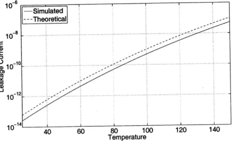
Normally leakage currents are small enough compared to transistor bias currents that they can be ignored. However, when transistors operate with tens of nano-amps at high temper-atures, leakage currents become significant compared to the bias levels. The temperature dependence of the leakage current will be described so that estimates of the magnitude of the leakage current and the parameters which affect it can be understood.
ID = AJs e kT - 1) (3.6)
The typical diode equation is shown in Eqn. 3.6. When the diode voltage (VD) is
negative the diode current is approximately equal to the saturation current (-AJs). This reverse current is typically on the order of femto-amps at room temperature, but it has significant temperature dependence.
qDhn? qDen(
s= N h+ (37)