HAL Id: hal-02271107
https://hal.archives-ouvertes.fr/hal-02271107
Submitted on 24 Apr 2020HAL is a multi-disciplinary open access archive for the deposit and dissemination of sci-entific research documents, whether they are pub-lished or not. The documents may come from teaching and research institutions in France or abroad, or from public or private research centers.
L’archive ouverte pluridisciplinaire HAL, est destinée au dépôt et à la diffusion de documents scientifiques de niveau recherche, publiés ou non, émanant des établissements d’enseignement et de recherche français ou étrangers, des laboratoires publics ou privés.
Oxygen incorporated during deposition determines the
crystallinity of magnetron-sputtered Ta3N5 films
M. Rudolph, I. Vickridge, E. Foy, J. Alvarez, Jean-Paul Kleider, D. Stanescu,
H. Magnan, N. Herlin-Boime, B. Bouchet-Fabre, T. Minea, et al.
To cite this version:
M. Rudolph, I. Vickridge, E. Foy, J. Alvarez, Jean-Paul Kleider, et al.. Oxygen incorporated dur-ing deposition determines the crystallinity of magnetron-sputtered Ta3N5 films. Thin Solid Films, Elsevier, 2019, 685, pp.204-209. �10.1016/j.tsf.2019.06.031�. �hal-02271107�
1
Oxygen incorporated during film growth determines the crystallinity of
magnetron-sputtered Ta3N5 films
M. Rudolph1,6, I. Vickridge2, E. Foy3, J. Alvarez4, J.-P. Kleider4, D. Stanescu5, H. Magnan5,
N. Herlin-Boime6, B. Bouchet-Fabre6, T. Minea1, M.-C. Hugon1
1 LPGP, UMR 8578 CNRS, Université Paris-Sud, Université Paris-Saclay, 91405 Orsay, France
2 INSP, Sorbonne Université, Université Pierre et Marie Curie, 75005 Paris
3 LAPA-IRAMAT, NIMBE, CEA, CNRS, Université Paris-Saclay, CEA Saclay, 91191
Gif-sur-Yvette, France
4 GeePs, CNRS UMR8507, CentraleSupelec, Univ Paris-Sud, Université Paris-Saclay, Sorbonne
Université, 91192 Gif-sur-Yvette, France
5 SPEC, CEA/CNRS, Université Paris-Saclay, 91191 Gif-sur-Yvette, France
6 NIMBE, CEA/CNRS, Université Paris-Saclay, 91191 Gif-sur-Yvette, France
Abstract
Ta3N5 belongs to the group of transition metal nitrides with the cation in a high formal oxidation
state. These are, in general, difficult to synthesize owing to the low reactivity of nitrogen. This
applies similarly to Ta3N5 that crystallizes only in the presence of oxygen during synthesis.
Typical preparation methods are ammonolysis of oxidized Ta or magnetron sputtering of a Ta
target in an atmosphere of Ar, N2 and O2. However, the thin films typically obtained by either
synthesis method are of varying degree of crystallinity and the parameters affecting the
crystallinity remain unclear. In this study, we identify oxygen to be the central driver for the
crystallinity of Ta3N5 thin films prepared by magnetron sputtering. While little oxygen in the
films yields the metallic δ-TaN phase, excess oxygen results in low crystallinity Ta3N5 or
2
limiting the oxygen supply to the sample during the deposition. Comparison with other studies
suggest a fundamental oxygen incorporation limit above which the crystallinity of Ta3N5 is
compromised. The most crystalline sample from this study contains 4.4 at.% of oxygen. It is
grown onto a Si(100) substrate, covered with a 30 nm-thick metallic Ta layer. Large Ta3N5
grains between 80 and 120 nm in size are obtained.
1 Introduction
Ta3N5 is a promising candidate as a photon absorber in solar water splitting devices because its
valence and conduction bands straddle the oxygen and hydrogen evolution potentials [1]. At
the same time, it can absorb a large part of the solar spectrum owing to its small band gap of
2.1 eV [1, 2]. In fact, it is very close to the assumed optimum band gap of around 2.0 eV, which
is the compromise between the fraction of absorbed sunlight and the electric potential necessary
to split water into oxygen and hydrogen [3]. One important parameter for the Ta3N5 photon
absorber regarding the application in view is a high degree of crystallinity. This is because
non-crystalline regions, in form of grain boundaries or amorphous content, represent sites of
recombination for photogenerated charge carriers, reducing the overall device efficiency.
However, Ta3N5 thin films prepared so far by ammonolysis or magnetron sputtering show
varying degrees of crystallinity and the central parameter to control the crystallinity remains
yet unclear.
The formation of Ta3N5 is triggered by oxygen incorporation [4,5,6]. This applies to both
principal preparation routes, ammonolysis and magnetron sputtering. Ammonolysis typically
requires an oxidized tantalum precursor that is annealed under a flow of NH3. In this process,
nitrogen diffuses into the material and partially replaces the oxygen anions in the lattice [7].
The process requires high temperatures (> 680° C) and can take up to several hours [8,9,10]. In
general, the sample crystallinity increases with the thermal budget [9]. Grain sizes obtained by
3
sizes between 17.3 nm and 17.7 nm and Dabirian et al. [9] observe average grain sizes between
22 nm and 36 nm.
Magnetron sputtering of a Ta target in a gas mixture of Ar, N2 and O2 is an alternative synthesis
route. It offers a reduced thermal budget compared to ammonolysis with crystalline samples
obtained at substrate temperatures between 400° and 600° C [11]. However, magnetron
sputtering at these temperatures often results in a low degree of crystallinity [5,6]. Crystallinity
improves by increasing the substrate temperature to values close to those necessary for
ammonolysis. Ishihara et al. achieve a higher degree of crystallinity of their
magnetron-sputtered Ta3N5 thin films by using a higher substrate temperature, i.e. 800° C, compared to the
onset temperature for crystallization found between 400° to 600° C [11]. Alternatively,
annealing sputtered Ta3N5 samples in NH3 at 750° C for 15h after the deposition is similarly
successful in improving the sample crystallinity[5].
The studies listed above suggest a strong effect of the thermal budget on the crystallinity of
Ta3N5 thin films, though its direct effect on the crystallinity is not conclusively proven. Possible
may also be an indirect correlation and we suggest the oxygen content in the film to link the
thermal budget with the crystallinity. We therefore focus our investigation on the isolated effect
of oxygen on the crystallinity of the samples. This is possible by magnetron sputtering, as the
oxygen incorporation can be tuned during the sputtering process while leaving all other process
parameters, in particular the thermal budget, constant. The oxygen content, calculated as the
ratio O/(Ta+N+O) and expressed in at.%, is quantified using Rutherford backscattering
spectrometry (RBS) and nuclear reaction analysis (NRA). The obtained sample composition is
then correlated with the crystalline structure from grazing-incidence X-ray diffraction
(GI-XRD). To support the results from GI-XRD, the surface is imaged by atomic force microscopy
(AFM) and scanning electron microscopy (SEM). Finally, two samples having different oxygen
4
2 Film preparation and characterization techniques
The films were prepared by ion-assisted growth using a balanced magnetron with two external
magnetic coils to increase the ion flux onto the substrate [12]. Measurements of the ion
saturation current together with the area density measurements from the ion beam analysis (see
below) revealed an ion-to-neutral flux ratio of 0.3 in standard balanced magnetron configuration
and 2.8 using the external magnetic coils. The magnetron was installed in a vacuum chamber
with a base pressure of < 5⋅10-4 Pa. The Ta target was of 99.95% purity and had a diameter of 10 cm. The power applied to the cathode was 80 W corresponding to a cathode potential of
-330 V. The cathode potential was intentionally kept small in order to limit the rate of high
energy (> 100 eV) Ar neutrals backscattered from the target, that risked to incorporate defects
into the growing film [13].
The films were deposited on polished monocrystalline Si(100) and Ta foil substrates. Films on
the Si substrate were used to determine their structure, elemental composition, crystallinity and
topography. Films on the Ta foil substrate were used to test their photoactivity in a
photoelectrochemical cell.
Prior to deposition, the substrates were cleaned in a bath of isopropanol for 5 min and then
blown dry with N2. They were then clamped onto a substrate holder and inserted into the
deposition chamber. The substrates were sputter-etched for 10 min at an effective DC bias of
-100 V by Arions from a radio-frequency plasma. At the same time, with a closed shutter in
front of the magnetron, the target was sputter-etched at 80 W in DC mode for 10 min in pure
Ar. Afterwards, the surface was conditioned by sputtering for further 10 min but using the gas
composition of the following deposition.
The samples were deposited at a pressure of 0.5 Pa. The N2 flowrate was 20 sccm, the O2
flowrate was varied between 0.0 sccm and 0.9 sccm and Ar was added to reach a total flowrate
5
the deposition, a 30 nm-thick metallic Ta interlayer was deposited at room temperature onto the
substrates in order to provide the same growth conditions for the Ta3N5 film on both types of
substrates. It is important to note that this layer had a considerable effect on the crystallinity of
the Ta3N5 phase as discussed below. Each Ta3N5 thin film was deposited to obtain a 250
nm-thick layer which took around 30 min. The nm-thickness was confirmed by using a mechanical
profilometer on the edge of a region shadowed during the deposition.
The composition of the samples was measured using ion beam analysis with the SAFIR
platform of Sorbonne Université. The 181Ta area density (AD) was determined using RBS at an α beam energy of 2000 keV. The AD of the underlying 30 nm-thick Ta layer was measured on a separate substrate and subtracted for the determination of the film composition. Minor levels
of Ar were found in the films by RBS (≈ 1 at.%), which were neglected for the analysis
presented here. The nitrogen and oxygen AD were determined by NRA using the nuclear
reactions 14N(d,α)12C at 1400 keV and 16O(d,p)17O at 850 keV.
The crystalline structure was determined by GI-XRD using a custom-built setup. It consisted
of a 30 µm × 50 µm thick X-ray beam from a Mo anode (λalpha = 0.071 nm) that was incident
on the sample at 0.5° to the sample surface. Diffracted rays were recorded using a
photo-sensitive plate that was digitized using a scanner. The software fit2d [14] was used to integrate
the spherical diffraction patterns resulting in the diffractograms presented here. The background
was intentionally not subtracted.
The photocurrent was measured in a custom-built photoelectrochemical cell in a three-electrode
configuration [15]. The sample was mounted as the working electrode, a Pt wire as a counter
electrode and an Ag/AgCl/sat. KCl as a reference electrode. The electrolyte was an aqueous
solution with 0.1 M K2SO4 and KOH added to obtain a pH of 13. Potential control and current
acquisition were done using a Princeton Applied Research 263A potentiostat. For photocurrent−voltage curves, the potential was swept from −0.4 to +0.4 V vs. Ag/AgCl/sat. KCl
6
with a rate of 50 mV/s. The sample was illuminated through a quartz window by intermittent
light from a Newport Xe arc lamp. It was equipped with an infrared filter to prevent the sample
from heating up. The irradiance at the sample position was 21 mW/cm2.
3 Thin film characterization
3.1 Elemental composition and crystallinity
The composition of the films is presented in Fig. 1 as a function of the O2 flowrate injected into
the reactor during the sputtering process. At 0 sccm O2, the thin film is saturated with nitrogen.
The sample contains 37.6 at.% of tantalum, 60.9 at.% of nitrogen and a small amount of oxygen.
Similar results are obtained by Sun et al. [16] for magnetron-sputtered Ta-N, who find an
increasing nitrogen content with increasing the N2 supply to the reactor. This trend continues
until the nitrogen incorporation saturates at around 60 at.% of nitrogen, a value very similar to
the 60.9 at.% found in our experiments. Stoichiometric Ta3N5, in comparison, contains 62.5
at.% of nitrogen, which is slightly higher.
The reason for the lower nitrogen content measured in our sample, compared to the ideal
composition of Ta3N5, can be explained by a small amount of oxygen incorporated. This
originates from the background O2 present in the deposition chamber even without intentionally
injecting O2 via the flowmeters. During deposition, this oxygen is preferentially incorporated
due to its lower free energy of formation [17]. Once incorporated, it prevents further uptake of
nitrogen to keep the charge balance between the anions and the Ta cation.
At an O2 flowrate between 0.1 and 0.6 sccm, the oxygen incorporated into the film increases
linearly. This indicates that the magnetron target is not yet in its poisoned state with respect to
oxygen, so that all O2 supplied to the process chamber is immediately gettered by sputtered Ta
7
levels of oxygen are incorporated into the film, due to a reduced Ta deposition rate from a
poisoned target [18].
Fig. 1: Elemental composition of samples prepared at varying O2 flowrates.
The crystallinity of the deposited films is measured on the same samples as those used to
determine the elemental composition. Without any intentional oxygen supplied to the reactor
during deposition (0 sccm O2), the metallic δ-TaN phase is obtained (Fig. 2). By increasing the
oxygen supply to 0.1 and 0.2 sccm O2, a phase mixture between δ-TaN and Ta3N5 appears.
Only at an O2 flow of 0.3 sccm, corresponding to an oxygen content of 4.4 at.% in the film, the
diffractogram shows a single phase Ta3N5 signature . The peaks match that of the orthorhombic
Ta3N5 structure (powder diffraction file 01-079-1533 from the International Centre for
Diffraction Data (ICDD) database). Note, that with the diffractometer used, we cannot
distinguish between the monoclinic [19] and the orthorhombic [20,21] Ta3N5 structure because
both have similar peak positions.
Increasing the O2 supply deteriorates the crystallinity of the sample. At 0.5 sccm of O2, the
diffractogram exhibits lower peak intensities. At even higher flowrates, the peaks vanish
completely. The sample deposited at 0.7 sccm O2 exhibits two broad halos around 23 nm-1 and
8
halos are similarly found by other authors studying Ta-O-N thin films [12,22,23] and can be
attributed to some remaining local order.
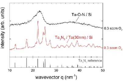
The samples presented above all have a 30 nm-thick Ta interlayer between the Si substrate and
the Ta3N5 thin film. This has a crucial influence on the crystallinity, which is illustrated by
depositing a film directly onto a Si(100) substrate. While the reference sample with a Ta
interlayer shows sharp diffraction peaks in GI-XRD experiments, the diffractogram of the
sample missing the Ta interlayer exhibits no peaks at all proving the lack of crystallinity
(Fig. 3). Possible explanations for this could be that the Ta interlayer represents a nucleation
layer for Ta3N5. Another possibility is that Si impurities in Ta-O-N prevent its crystallization
to Ta3N5. Si-Ta alloy formation is observed at temperatures of 700° C [24], close to the 600° C
substrate temperature used in this study. A Ta interlayer could therefore act as a diffusion
barrier, keeping Si out of the Ta3N5 film. Similarly to our experiments, de Respinis et al. [25]
sputtered on top of their fused silica substrate a 5 nm-thick layer of Ti, before depositing
metallic Ta that was subsequently oxidized and nitrided to form Ta3N5. They mention the
possibility that the Ti interlayer may affect the crystallization behavior of Ta3N5 without giving
further details. The Ti interlayer in their case could therefore similarly act as a diffusion barrier
against the Si that is present in their fused silica substrate.
3.2 Morphology and surface topography
Two selected samples deposited at 0.3 and 0.5 sccm O2 are imaged by SEM (Fig. 4). The surface
of the first one is densely covered by crystallites with diameters between 80 nm and 120 nm.
As no other phase as Ta3N5 is detected in the diffractograms (Fig. 2), the crystallites likely have
the Ta3N5 structure. In between crystallites, the image shows some featureless areas that we
assign to small amounts of an amorphous matrix, indicating that further fine-tuning of the
oxygen content in the films may be possible. The cleaved cross-section of the sample shows a
9
throughout the film thickness. On the other hand, the sample deposited at a higher O2 flowrate
(0.5 sccm) shows a reduced density of crystallites. The crystallites also appear less pronounced
and their boundaries vanish in a dominating featureless matrix. Similarly, the cleaved
cross-section is flat and without perceivable texture compared to the sample deposited at a lower O2
flowrate. The loss of crystallinity at higher O2 flowrates seen in the SEM images matches well
with the trend observed in the diffractograms.
Fig. 2: GI-XRD diffractograms as a function of O2 flowrate supplied during the deposition. The
reference is taken from the powder diffraction file 01-079-1533 (Ta3N5) and 01-089-5196
(δ-TaN) in the ICDD database. The narrow peak on the sample deposited at a flow of 0.6 sccm
10
Fig. 3: Influence of a 30 nm-thick Ta interlayer on the crystallinity of the Ta3N5 thin films
deposited at 0.3 sccm O2.
Fig. 4: Scanning electron microscopy images of the sample deposited at O2 flowrates of 0.3
sccm (top) and at 0.5 sccm (bottom), respectively. The cross-section images on the left exhibit the 30 nm-thick Ta interlayer.
11
AFM images reveal the topography of the surface (Fig. 5). At a low O2 flowrate (0.2 sccm), the
surface is rough. While the highest point lies 63 nm above the baseline, most of the surface lies
between 0 and about 30 nm. The comparison with the SEM images suggests, that this roughness
is due to crystallites peeking out of the surface. As this sample has a dominating Ta3N5 signature
according to its diffractogram, we suggest that these are mainly Ta3N5 crystallites. Increasing
the O2 flowrate decreases the roughness, in line with the observation from the SEM images,
that when crystallinity is lost, the surface becomes increasingly flat due to a dominating
amorphous content. At the highest O2 flowrate of 0.7 sccm, the sample becomes completely flat
with the highest point at only 3 nm above the baseline. This is in line with the observation from
GI-XRD, i.e. the sample is nanocrystalline or amorphous.
The sample deposited at a flowrate of 0.6 sccm still contains some Ta3N5 crystallites, according
to its diffractogram (Fig. 2). The AFM image, however, shows a flat surface covered with what
appears as dips or holes. This sample with its high content of oxygen (9.6 at.%) is at the border
of a vanishing Ta3N5 structure. The surface may therefore easily be changed by a small amount
of extra oxygen. This is likely supplied at the end of the deposition process. When the
magnetron is switched off, the deposition of fresh Ta onto the growing film and the reactor
walls stops and so does the gettering of oxygen from the gas phase on these surfaces. At this
moment, the oxygen concentration in the reactor rises during a short period of an estimated few
tens of seconds, while the sample is still at an elevated temperature. The surface can therefore
continue to oxidize causing the surface structure to collapse. This supports the conclusion from
above that the Ta3N5 structure cannot tolerate excessive amounts of oxygen.
The experiments presented here show a wide range of degrees of crystallinities of Ta3N5 thin
films. It is important to note that each film is deposited with the same thermal budget during
the sputtering process and by adjusting only the O2 flowrate and with that, the oxygen content
12
magnetron-sputtered Ta3N5 thin films is determined by the oxygen incorporation into the film,
which can be tuned by the oxygen supplied during the sputtering process.
Fig. 5: Surface topology measured by AFM as a function of O2 flowrate. Note the different
height scales on the right of each image.
3.3 Photocurrent measurements
Photocurrent measurements in a photoelectrochemical cell under intermittent light prove the
photoactivity of the deposited Ta3N5 films (Fig. 6). The experiments are done with two samples
deposited at 0.3 sccm and 0.5 sccm O2 flowrate, thus containing 4.4 at.% and 7.7 at.% of
oxygen, respectively. According to their diffractograms and SEM images, these are
13
The photoactivity of these samples is evaluated in five consecutive scans. For both samples, the
photocurrent decreases strongly with each repetition of the experiment. This is due to a
self-oxidation of the surface by photogenerated holes as suggested by Ishikawa et al. [26]. He et al.
[27] show that the oxidation is self-limiting and restricted to a few nm. However, the thin oxide
pins the Fermi levels at the surface, reducing the band bending. As a consequence, charge
carrier separation becomes successively less efficient. Finally, the photocurrent practically
ceases. In this state, the surface is limiting the photocurrent and the enhanced bulk properties
of the sample containing more oxygen do not make a difference any more. Mitigation methods
aim to separate the Ta3N5 photoabsorber from the electrolyte which in some cases can also
accelerate the hole transfer from the photoanode to the electrolyte [5,9,27,28]. These layers are
not further investigated here.
Comparing the first photocurrent-voltage curves obtained with each sample, the high
crystallinity sample (deposited at 0.3 sccm O2) shows a lower photocurrent than the low
crystallinity one (deposited at 0.5 sccm O2). The latter contains more oxygen, which is known
to widen the band gap [6,29,30]. Therefore, on the one hand, it can be expected to absorb less
photons of the light spectrum which would result in a lower density of photogenerated charge
carriers. On the other hand, the larger band gap could induce a higher open circuit voltage
promoting the charge carrier transfer to the electrolyte. The higher photocurrent for the
oxygen-rich sample suggests that latter effect dominates here.
Nevertheless, our observation is in discrepancy with other authors that observe the inverse
effect. Yokohama et al. [5] increase the initial low crystallinity of their sputtered samples in the
as-processed state by annealing them in NH3. They observe a strong increase in photocurrent
after this treatment and assign it to the improved crystallinity. Li et al. [31] prepare their Ta3N5
14
1000° C instead of 850° C, which they attribute partially to an improved interface between the
semiconductor and the substrate, and partially to a higher crystallinity.
Our observation that the sample deposited at 0.5 sccm O2 shows a higher photocurrent can be
understood by assuming that both samples still contain a high density of defects that acts as
sites of carrier recombination. Such a material would have a small minority carrier diffusion
length, i.e. the contribution to the photocurrent from minority carriers originating from the bulk
is reduced. In this case, the photocurrent would arise from the surface of the photoanode where
carriers are immediately separated by the electric field in the space charge layer and thus escape
recombination. In this case, a slightly larger band gap caused by a higher oxygen content in the
film deposited at 0.5 sccm O2 would not be detrimental as the surface would be sensitive in
particular to UV and blue light. The higher initial photocurrent of this sample could then be
attributed to a higher open circuit voltage that results in a more efficient hole transfer to the
electrolyte.
The origin of the defects in the Ta3N5 thin film could be the sputtering process that is known to
induce material defects from the bombardment of energetic particles. These can be negative
ions, e.g. O-, that are accelerated in the plasma sheath above the cathode [32] or neutrals
backscattered from the cathode [13]. An annealing treatment could help to reduce the defect
density in the bulk. Note that such a treatment would be different in temperature and duration
from the NH3 annealing done by other authors to prepare Ta3N5 samples, as the purpose is not
15
Fig. 6: On-Off photocurrent curves for two selected samples deposited at 0.3 sccm and
0.5 sccm O2 flowrate.
3 Discussion
The study identifies oxygen being the main driver for the degree of crystallinity of
magnetron-sputtered Ta3N5 thin films. Henderson et al. [10] report on the crystallinity of Ta3N5 samples
prepared by ammonolysis. By varying temperature and duration of the process, they find that
crystallinity is lost by increasing the oxygen content of their samples, similar to the results of
this study. Their sample with the highest crystallinity contains 2.9 at.% of oxygen, which is in
the same order of magnitude as the 4.4 at.% of oxygen found in our most crystalline sample.
The similarity of the value, despite the different synthesis methods, suggests that Ta3N5
crystallinity is fundamentally compromised at oxygen contents above a few at.%.
An oxygen incorporation limit in Ta3N5 explains well the high temperatures and long process
durations, i.e. a high thermal budget, necessary to obtain high crystallinity Ta3N5 by
ammonolysis. The thermal budget is necessary to diffuse excess oxygen out of a Ta-O precursor
and to substitute it by nitrogen. In magnetron sputtering, the oxygen-nitrogen substitution is not
necessarily required due to the simultaneous incorporation of oxygen and nitrogen into the film.
This allows a lower thermal budget for the onset of Ta3N5 crystallization with temperatures
16
Still, high substrate temperatures of up to 800° C are necessary to reach a high degree of
crystallinity in experiments done by Ishihara et al. [11]. A possible explanation for this
observation could be a high oxygen content in the films deposited at low substrate temperature.
Similarly could the low crystallinity of magnetron-sputtered Ta3N5 samples prepared by
Yokohama et al. [5] be explained by excess oxygen in the as-deposited films. Both Ishihara et
al. [11] and Yokoyama et al. [5] use a total pressure similar to our study. However, in both
studies, they use an O2 partial pressure of 0.01 Pa, and between 0.013 and 0.07 Pa, respectively.
These values are much higher by at least a factor of 3 compared to the 0.003 Pa used in our
study for the most crystalline sample (deposited at 0.3 sccm O2). In addition, the deposition rate
in Yokoyama et al. is less than half our deposition rate (100 nm in 30 min [5] compared to 250
nm in 30 min in this study). As these films grow more slowly while being subjected to a higher
O2 partial pressure, they likely have a higher oxygen content compared to our most crystalline
sample. Excess oxygen could thus explain the low crystallinity of their samples. In a similar
way can our findings be used to explain improvements in crystallinity. Yokoyama et al. improve
the crystallinity of their as-processed samples by a post-deposition annealing treatment in NH3
[5]. This improved crystallinity can be attributed to a lower oxygen content in the films, as the
samples are expected to lose oxygen during annealing. Ishihara et al. enhance the crystallinity
by raising the substrate temperature which lowers the oxygen content in the films [11]. This is
because a higher substrate temperature increases the reactivity of nitrogen which eases its
incorporation into the growing film. As the oxygen supply to the growing film is limited, the
oxygen/nitrogen ratio in the film is lowered. These examples show that our findings can explain
changes in crystallinity of Ta3N5 thin films by variations of the oxygen content in the films.
The conclusion of this paper that oxygen determines the degree of crystallinity of Ta3N5 thin
17
observed correlation between the thermal budget and the sample crystallinity, however, is only
an indirect one with the oxygen content in the film being the link between the two.
The fact that Ta3N5 tolerates only a limited amount of oxygen, has important implications for
the application of this material as a photon absorber in solar water splitting devices. Many
properties of Ta-O-N thin films can be tuned by varying the oxygen-to-nitrogen ratio, such as
the band gap [6,33] and electronic properties [6]. However, if a Ta3N5 crystalline structure is
desired, the range over which these properties can be tuned is limited. This applies especially
to the position of the band edges that are important for achieving solar water splitting. The
valence band edge of oxygen-free Ta3N5 is predicted to be too low with respect to the O2/H2O
potential. Only with high oxygen doping, this band edge is sufficiently shifted [30] which may,
however, not be compatible with a crystalline structure according to the findings of this paper.
4 Conclusion
This work identifies the oxygen content in Ta3N5 as the key parameter affecting the crystallinity
of Ta3N5 thin films. A high level of oxygen incorporated into a film results in a low degree of
crystallinity. This manifests in large amorphous regions into which few Ta3N5 crystallites are
embedded. By lowering the oxygen supply during deposition, highly crystalline samples are
obtained. This is possible by magnetron-sputtering as it allows a precise control of the oxygen
incorporated homogeneously throughout the film thickness. The highest crystallinity is
obtained for a sample containing 4.4 at.% of oxygen. This film exhibits large grains between
80 and 120 nm in size. The results show that the variations in degree of crystallinity of Ta3N5
thin films, observed by other authors, can largely be explained by different levels of oxygen
incorporated into the material. This suggests a fundamental limit of oxygen incorporation
before the crystallinity of Ta3N5 is compromised.
18
The authors thank the Centre National de la Recherche Scientifique (CNRS) for funding of this
activity under grant agreement ANR-13-IS09-0003-01. The authors would like to thank Patrick
Bonnaillie for the SEM images.
References
[1] W.-J. Chun, A. Ishikawa, H. Fujisawa, T. Takata, J. N. Kondo, M. Hara, M. Kawai, Y.
Matsumoto, K. Domen, Conduction and valence band positions of Ta2O5, TaON, and Ta3N5
by UPS and electrochemical methods, J. Phys. Chem. B 107, 1798-1803, 2003.
[2] J. M. Morbec, I. Narkeviciute, T. F. Jaramillo, G. Galli, Optoelectronic properties of
Ta3N5: A joint theoretical and experimental study, Phys. Rev. B 90, 155204, 2014.
[3] A.B. Murphy, P. R. F. Barnes, L. K. Randeniya, I. C. Plumb, I. E. Grey, M. D. Horne, J.
A. Glasscock, Efficiency of solar water splitting using semiconductor electrods, Int. J.
Hydrog. Energy 31, 1999-2017, 2006.
[4] M. Hara, E. Chiba, A. Ishikawa, T. Takata, J. N. Kondo, K. Domen, J. Phys. Chem. B
107, 13441-13445, 2003.
[5] D. Yokoyama, H. Hashiguchi, K. Maeda, T. Minegishi, T. Takata, R. Abe, J. Kubota, K.
Domen, Ta3N5 photoanodes for water splitting prepared by sputtering, Thins Solid Films
519, 2087-2092, 2011.
[6] M. Rudolph, D. Stanescu, J. Alvarez, E. Foy, J.-P. Kleider, H. Magnan, T. Minea, H.
Herlin-Boime, B. Bouchet-Fabre, M.-C. Hugon, The role of oxygen in magnetron-sputtered
thin films of Ta3N5 for the photoelectrolysis of water, Surf. Coat. Technol. 324, 620-625,
2017.
[7] D. Lu, G. Hitoki, E. Katou, J. N. Kondo, M. Hara, K. Domen, Porous single-crystalline
19
[8] B. A. Pinaud, A. Vailionis, T. F. Jaramillo, Controlling the structural and optical
properties of Ta3N5 films through nitridation temperature and the nature of the Ta metal,
Chem. Mater 26, 1576-1582, 2014.
[9] A. Dabirian, R. van de Krol, Resonant optical absorption and defect control in Ta3N5
photoanodes, Appl. Phys. Lett. 102, 033905, 2013.
[10] S. J. Henderson, A. L. Hector, Structural and compositional variations in Ta3N5
produced by temperature amaonolysis of tantalum oxide, J. Sol. State Chem., 179, 3518-3524,
2006.
[11] A. Ishihara, S. Doi, S. Mitsushima, K.-I. Ota, Tantalum (oxy)nitrides prepared using
reactive sputtering for new nonplatinum cathodes of polymer electrolyte fuel cell,
Electrochim. Acta 53, 5442-5450, 2008.
[12] M. Rudolph, A. Demeter, E. Foy, V. Tiron, L. Sirghi, T. Minea, B. Bouchet-Fabre, M.-C.
Hugon, Improving the degree of crystallinity of magnetron-sputtered Ta3N5 thin films by
augmenting the ion flux onto the substrate, Thin Solid Films, 636, 48-53, 2017.
[13] M. Rudolph, D. Lundin, E. Foy, M. Debognie, M.-C. Hugon, T. Minea, Influence of
backscattered neutrals on the grain size of magnetron-sputtered TaN thin films, Thin Solid
Films 658, 46-53, 2018.
[14] A. P. Hammersley, FIT2D: a multi-purpose data reduction, analysis and visualization
program, J. Appl. Cryst. 49, 646-652, 2016.
[15] Rioult M., Magnan H., Stanescu D., Barbier A., Single Crystalline Hematite films for
Solar Water Splitting: Ti Doping and Thickness Effects, J. Phys. Chem. C, 118, 3007–3014,
2014.
[16] X. Sun, E. Kolawa, J.-S. Chen, J. S. Reid, M-A. Nicolet, Properties of reactively
20
[17] A. Fuertes, Synthesis and properties of functional oxynitrides – from photocatalysts to
CMR materials, Dalton Trans. 39, 5942 -5948, 2010.
[18] S. Berg, T. Nyberg, Fundamental understanding and modeling of reactive sputtering
processes, Thin Solid Films 476, 215-230, 2005.
[19] N. Terao, Structure of tantalum nitrides, Jpn. J. Appl. Phys. 10, 2, 248-259, 1971.
[20] J. Strähle, Die Kristallstruktur des Tantal(V)-nitrids Ta3N5, Z. Anorg. Allg. Chem. 402,
47-57, 1973.
[21] N. E. Brese, M. O’Keefe, P. Rauch, F. J. Disalvo, Structure of Ta3N5 at 16 K by
time-of-flight neutron diffraction, Acta Cryst. C47, 2291-2294, 1991.
[22] M. Stavrev, D. Fischer, C. Wenzel, K. Drescher, N. Mattern, Crystallographic and
morphological characterization of reactively sputtered Ta, Ta-N and Ta-N-O thin films, Thin
Solid Films 307, no. 1-2, 79 – 88, 1997.
[23] A. Bousquet, F. Zoubian, J. Cellier, C. Taviot-Gueho, T. Sauvage, E. Tomasella,
Structural and ellipsometric study on tailored optical properties of tantalum oxynitride films
deposited by reactive sputtering, J. Phys. D: Appl. Phys. 47, 475201, 2014.
[24] K. Holloway, P. M. Fryer, Tantalum as a diffusion barrier between copper and silicon,
Appl. Phys. Lett. 57, 1736-1738, 1990.
[25] M. de Respinis, M. Fravventura, F. F. Abdi, H. Schreuders, T. J. Savenije, W. A. Smith,
B. Dam, R. van de Krol, Oxynitrogenography : Controlled synthesis of single-phase tantalum
oxynitride photoabsorbers, Chem. Mater. 27, 7091-7099, 2015.
[26] A. Ishikawa, T. Takata, J. N. Kondo, M. Hara, K. Domen, Electrochemical behavior of
thin Ta3N5 semiconductor film, J. Phys. Chem. B 108, 11049 – 11053, 2004.
[27] Y. He, J. Thorne, C. Hao Wu, P. Ma, C. Du, Q. Dong, J. Guo, , D. Wang, What limits the
21
[28] Y. Li, L. Zhang, A. Torre-Pardo, J. M. Gonzáles-Calbet, Y. Ma, P. Oleynikov, O.
Terasaki, S. Asahina, M. Shima, D. Cha, L. Zhao, K. Takanabe, J. Kubota, K. Domen,
Cobalt-Phosphate-modified barium-doped tantalum nitride nanorod photoanode with 1.5%
solar energy conversion efficiency, Nat. Commun. 4:2566, 2013.
[29] K. Maeda, K. Domen, New non-oxide photocatalysts designed for overall water splitting
under visible light, J. Phys. Chem. C 111, 7851-7861, 2007.
[30] M. Harb, P. Sautet, E. Nurlaela, P. Raybaud, L. Cavallo, K. Domen, J.-M. Basset, K.
Takanabe, Tuning the properties of visible-light-responsive tantalum (oxy)nitride
photocatalysts by non-stoichiometric compositions: a first-principles viewpoint, Phys. Chem.
Chem. Phys. 16, 20548-20560, 2014.
[31] Y. Li, T. Takata, D. Cha, K. Takanabe, T. Minegishi, J. Kubota, K. Domen, Vertically
aligned Ta3N5 nanorod arrays for solar-driven photoelectrochemical water splitting, Adv.
Mater. 25, 125-131, 2013.
[32] S. Mráz, J. M. Schneider, Influence of the negative oxygen ions on the structure
evolution of transition metal oxide thin films, J. Appl. Phys. 100, 023503, 2006.
[33] A. Bousquet, F. Zoubian, J. Cellier, C. Tavio-Gueho, T. Sauvage, E. Tomasella,
Structural and ellipsomtetric strudy on tailored optical properties of tantalum oxynitride films