HAL Id: hal-01004508
https://hal.archives-ouvertes.fr/hal-01004508
Submitted on 11 Jun 2014
HAL is a multi-disciplinary open access
archive for the deposit and dissemination of
sci-entific research documents, whether they are
pub-lished or not. The documents may come from
teaching and research institutions in France or
abroad, or from public or private research centers.
L’archive ouverte pluridisciplinaire HAL, est
destinée au dépôt et à la diffusion de documents
scientifiques de niveau recherche, publiés ou non,
émanant des établissements d’enseignement et de
recherche français ou étrangers, des laboratoires
publics ou privés.
Analysis and optimization of a novel high voltage striped
STI-LDMOS transistor on SOI CMOS technology
Gaëtan Toulon, Ignacio Cortes, Frédéric Morancho, Abdelhakim Bourennane,
Karine Isoird
To cite this version:
Gaëtan Toulon, Ignacio Cortes, Frédéric Morancho, Abdelhakim Bourennane, Karine Isoird. Analysis
and optimization of a novel high voltage striped STI-LDMOS transistor on SOI CMOS technology.
International Seminar on Power Semiconductors (ISPS 2012), Aug 2012, Pragues, Czech Republic.
pp.122-128. �hal-01004508�
Analysis and optimization of a Novel High Voltage Striped
STI-LDMOS Transistor on SOI CMOS Technology
G. Toulon
1.2, I. Cortés
3, F. Morancho
1.2A. Bourennane
1.4, K. Isoird
1.4,
1CNRS; LAAS; 7, Avenue du Colonel Roche; F-31400 Toulouse, France
2
Univ de Toulouse, LAAS, F-31400 Toulouse, France
3
Instituto de Microelectrónica de Barcelona (IMB-CNM) CSIC, Campus UAB, 08193 Bellaterra, Barcelona, Spain
4 Univ de Toulouse, UPS, LAAS, F-31400 Toulouse, France
Abstract
This paper analyses the static and dynamic characteristics of a novel n-type lateral-double-diffused MOS (LDMOS) with a striped Shallow Trench Isolation (STI) structure – called Striped STI-LDMOS – for switching applications in the 100-150 voltage range by means of 3D TCAD numerical simulations. The proposed structure based on a 0.18µm SOI CMOS technology and defined with STI strips and gate field plate fingers located on top of the defined STI, exhibits much lower gate-to-drain (CGD) capacitances and gate charge (Qg) and a better electrical safe operating area (SOA) as compared with a conventional STI-LDMOS counterpart.
Keywords: LDMOS transistor, Shallow Trench Isolation, safe operating area, gate-to-drain capacitance,
SOI, TCAD simulations.
INTRODUCTION
In smart power technology, where power devices are associated with CMOS and analogic circuits on the same chip, LDMOS transistors have proven to be the best suited power switch thanks to their ease of integration and
isolation with CMOS technology [1]. For lithography
resolution of 0.25µm and lower, the LOCOS oxidation has evolved to more precise shallow trench isolation (STI) oxidation, leading to the development of new designs of
LDMOS transistors [2]. The gain enhancement in CMOS
technology due to lithography size reduction is difficult to reach in power LDMOS due to the presence of the drift region, also called lightly doped drain (LDD) region,
necessary for high voltage specificity. Static
characteristics, such as breakdown voltage (VBR) and
specific on-state resistance (Ron-sp) are specially linked to
the drift region length (LLDD), in the well known VBR/Ron-sp
trade-off. Several techniques have been proposed so far to improve this trade-off, such as RESURF effect [3] or the
superjunction concept [4]. As for dynamic characteristics,
the LDMOS switching performance is not only limited by
its specific on-state resistance (Ron-sp), but also by the gate
charge (Qg) and inter-electrode capacitances for a given
VBR value. However, other electrical characteristics, such
as the safe operating area (SOA) have to be taken into account during the optimization of LDMOS transistors, because device geometrical and technological parameters, especially those concerning the channel/STI region definition, have a direct influence on the device
ruggedness [5]. Hence, both reliability and switching
performance should be optimized at the same time.
Different LDMOS transistors with STI in the LDD region (STI-LDMOS) have previously been extensively analyzed by numerical simulations [6, 7] and experimentally [7]. However, their dynamic characteristics are quite limited because of their inherent gate capacitances. The use of lateral gates and field plate on top of STI strips [8], successfully demonstrated on medium voltage LDMOS
(VBR < 40V), can highly reduce these parasitic
capacitances. Nevertheless, based on the authors‘ knowledge, this kind of structure has never been optimized for high voltage applications. In this sense, this work is addressed to analyze a new 150V voltage class
power LDMOS design structure in terms of VBR/Ron-sp
trade-off, Ron×Qg figure of merit (FOM), gate capacitance
evolution and safe operating area by means of 3D TCAD simulations.
STRUCTURES DESCRIPTION
Figure 1 shows the schematic cross section of the LDMOS transistors investigated in this paper: the proposed Striped STI-LDMOS (a) and the conventional STI-LDMOS (b), which are based on a 0.18µm smart power technology on thin-SOI substrate. All the analyzed LDMOS structures have the same thin-SOI substrate with a SOI layer (TSOI) and buried oxide (TBOX) thickness of
1.6µm and 1µm, respectively. The same LLDD of 7µm for
a total cell length (Lcell) of 11.5µm is also considered.
Both LDMOS structures require a previously formed STI block in the drift region before the P-well and N-well
implantation definition. A STI length (LSTI) of 4µm which
(W), respectively, is considered in conventional structure (see figure 1 (b)) Unlike the conventional STI-LDMOS, the STI strips in the novel structure (see Figure 1 (a)) are defined partially covering the device width (W). Hence, the cell width of the Striped STI-LDMOS can be described as the addition of the region covered by the STI (WSTI) and the region not covered by the STI (WSi). It is
also noticeable the STI extension along the P-well diffusion. Hense, the poly-gate block, deposited only on the top of the STI strips, defines not only the gate electrode but also the field plate above the N-drift region. The total poly-gate length over the STI is then described as the addition of the poly-gate length covering the P-well diffusion where the inversion channel is formed (Lchannel)
and the poly gate covering the N-drift region which acts as a gate field plate (LFP).
Figure 1: Schematic cross section of the (a) proposed striped STI-LDMOS and (b) conventional STI-LDMOS structures
A simulation result of the electron concentration distribution in the channel region of the striped STI-LDMOS is plotted in figure 2. As clearly observed, the channel inversion layer is laterally formed along the sidewall of the STI/P-well interface. The distance between
poly-gate and STI edge (Wox) determines the effective
gate oxide thickness and consequently the threshold voltage of this analyzed structure. On the other hand, the main portion of the inversion layer is mainly present on the top surface of the STI sidewall thanks to the higher
permittivity of the nitride spacer [9], but also on the
sidewall and, in a lesser extend, in the bottom of the STI.
Figure 2: Electron distribution in the channel region of the striped STI-LDMOS
TCAD SIMULATIONS RESULTS
VBR/Ron-sp trade-off 0.6 0.8 1.0 1.2 1.4 1.6 1.8 2.0 2.2 70 80 90 100 110 120 130 140 150 160 170 VBR (V )
N-drift doping concentration (1×1016 cm-3) Striped STI-LDMOS (WSi = 0.6µm, WSTI = 0.8µm) STI-LDMOS
WFP = 0.2µm LSTI = 4µm
WFP = 0.4µm
WFP = 0.6µm
Solid lines : VBR Doted lines : Ron-sp
ΔLPoly = LFP = 1.5µm 1.5 2.0 2.5 3.0 3.5 4.0 Spe cif ic o n-s tat e r esi sta nce ( m Ω× cm 2 ) 0.6 0.8 1.0 1.2 1.4 1.6 1.8 2.0 2.2 70 80 90 100 110 120 130 140 150 160 170 VBR (V )
N-drift doping concentration (1×1016 cm-3)
ΔLPoly = LFP = 2.5µm 1.5 2.0 2.5 3.0 3.5 4.0 Spe cifi c on -sta te res ista nce ( m Ω× cm 2 ) (b) (a)
Figure 3: Ron-sp/VBR trade-off as a function of the N-drift
doping concentration and WFP values considering different ΔLPoly
and LFP values of (a) 1.5µm and (b) 2.5µm in the STI-LDMOS
Figure 3 shows the VBR/Ron-sp trade-off comparison
between both analyzed LDMOS structures as a function of the N-drift doping concentration, where different values of the gate field plate width (WFP) and length (LFP) are
considered in the case of the Striped STI-LDMOS. The lower Ron-sp/VBR trade-off results exhibited by the Striped
STI-LDMOS structure compared to the conventional structure is derived by the high electric field reached at the end of the channel, which limits VBR, and by the worse
gate drift current transition, which limits the Ron-sp. The
WFP parameter, which does not affect the Ron-sp
characteristics, has a strong influence on VBR evolution.
The observed degradation of VBR as WFP increases is due
to the increase in the electric field along the STI/silicon interface because of the reduction of the STI width not covered by the poly field plate. On the other hand, the
increase of LFP will reduce the Ron-sp thanks to an enhanced
field effect action in the N-drift region. It leads, however, to a degradation of the VBR because of the worse electric
field distribution in the drift region.
The effective gate oxide, corresponding to the
combination of the gate oxide thickness (Tox, see figure 1
(b)) and the spacing distance between poly gate and STI
edge (Wox) leads to a higher threshold voltage (VT) in the
Striped STI-LDMOS, as represented in the transfer function of figure 4. Hence, the VT increase, along with
the lower area for the inversion layer path and the bad gate to drift current transition, contributes to the worse Ron-sp
results as compared with the conventional structure,
specially at low Vgs values as observed in figure 4.
However, the better linearity of the transfer characteristics make the striped STI-LDMOS a good candidate for radio-frequency applications. 0 2 4 6 8 10 0 1 2 3 4 Id ( 1 × 10 -6 ) (A/ µ m) Vgs (V) STI-LDMOS (LSTI=4µm)
Striped STI-LDMOS (WSTI=0.8µm; WSi=0.6µm; WFP=0.4µm)
Vds=0.1V
Figure 4: Drain current as a function of Vgs for both analyzed
STI-LDMOS structures.
Dynamic performance
The gate charge of power MOS transistors is representative of their switching losses. As a consequence,
the gate charge value (Qg) has then to be reduced in order
to improve the switching performances. The figure 5 represents the gate voltage evolution as a function of gate
charge of both LDMOS optimized in terms of VBR/Ron-sp
trade-off. The simulations have been carried out with the transistor switching on a resistive load and with its gate connected to a current generator. Consequently the charge
Qg is proportional to the switching time.
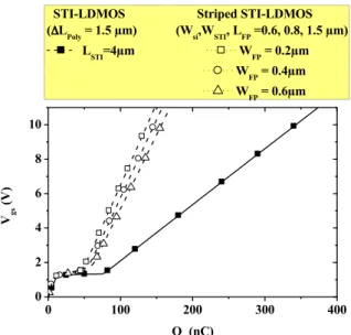
0 100 200 300 400 0 2 4 6 8 10 Vgs (V) Qg (nC)
STI-LDMOS Striped STI-LDMOS (ΔLPoly = 1.5 µm) (Wsi,WSTI, LFP =0.6, 0.8, 1.5 µm)
LSTI=4µm WFP = 0.2µm
WFP = 0.4µm
WFP = 0.6µm
Figure 5: Gate voltage versus gate charge and Ron×Qg FOM
As observed in figure 5, in spite of the higher Ron-sp values
(see figure 3 and 4), lower Ron×Qg FOM can be obtained
in the analysed in the Striped STI-LDMOS (see table 1) due to lower poly-gate interaction with the P-well region surface. Parameter value Ron× Qg STI-LDMOS ΔLPoly = 1.5 µm 0.552 Striped STI-LDMOS LFP = 0.2 µm 0.397 LFP = 0.4 µm 0.421 LFP = 0.6 µm 0.462
Table 1: Ron×Qg FOM comparison for different parameter
values
Other important indicator is the comparison of the Cgd
evolution as a function of the applied Vgd by means of
small-signal simulations, illustrated in figure 6 where a
Cgd peak value five fold lower than the conventional
structure is achieved in the Striped STI-LDMOS. As a consequence, a significantly reduction of Qg and Cgd can
be obtained, so that better switching performance is reached in the Striped STI-LDMOS structure. Moreover,
considering that the Ron-sp is independent of the WFP
parameter, an improvement of Ron×Qg FOM can be
0 2 4 6 8 10 0.2 0.4 0.6 0.8 1.0 1.2 1.4 1.6 1.8 2.0 Cgd ( 1 × 10 -1 5 )(F/ µ m) VGD (V) Striped STI-LDMOS (W Si = 0.6µm, WSTI = 0.8µm WFP=0.2µm)
Conventional STI-LDMOS (LSTI = 4µm)
Vds = 15V
Figure 6: Cgd as a function of Vgd for both LDMOS structures
Safe operating area (SOA)s
The body current (Ibody) evolution vs Vgs at high applied Vd
values is a good indication for the evaluation of the safe
operating area of the LDMOS structures [10, 11]. Then, in
order to determine the Ibody, a separated body contact is
placed in all the simulated structures. The comparison of
the simulated results form figure 7 shows the typical Ibody
vs Vgs characteristics curve in LDMOS transistors, where
a first Ibody peak at low Vgs values is observed. This Ibody
peak is specially related with the increase of e-/h+ pairs generated by impact ionization at the P-well/N-well junction in the channel region. This peak is proportional to the applied Vds [10]. According to figure 7, WFP plays
an important role in on the Ibody first peak in Striped
STI-LDMOS. On the other hand, the Ibody peak is followed by
an Ibody valley characteristic due to the reduction of the
electric field at the P-well/N-well junction region as Vgs
increases. Finally, beyond the valley, the curve exhibits a
Ibody positive slope up, which is more related to the Kirk
effect at high Vgs values [10, 11].
0 2 4 6 8 10 12 0 5 10 15 20 25 30 Ibo dy ( 10 -9 A/ µ m ) V gs (V)
STI-LDMOS Striped STI-LDMOS (WSi = 0.6µm, WSTI = 0.8µm)
L STI = 4µm WFP = 0.2µm W FP = 0.4µm W FP = 0.6µm Vds = 60V
Figure 7: Ibody characteristics vs Vgs for both LDMOS
structures at high applied Vds of 60V
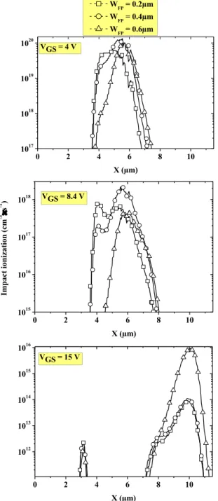
The electric field distribution and impact ionization generation along the STI/silicon interface of the Striped
STI-LDMOS at three Vgs values, corresponding to the first
Ibody bump (Vgs=4V), the Ibody valley (Vgs=8.4V), and the
current slope-up (Vgs=15V) are plotted in figures 8 and 9,
respectively. 0 2 4 6 8 10 0.0 0.5 1.0 1.5 2.0 X (µm) WFP = 0.2µm WFP = 0.4µm WFP = 0.6µm Vgs = 4 V 0 2 4 6 8 10 0.0 0.5 1.0 1.5 2.0 El ec tr ic fi el d (1 × 10 5 V /c m ) X (µm) Vgs = 8.4 V 0 2 4 6 8 10 0.0 0.5 1.0 1.5 2.0 X (µm) Vgs = 15 V
Figure 8: Electric field distribution along the STI/SOI interface for different values of the WFP at three different Vgs in
0 2 4 6 8 10 1012 1013 1014 1015 1016 X (µm) VGS = 15 V 0 2 4 6 8 10 1015 1016 1017 1018 Im pac t io niz ati on (cm -3 × s -1 ) X (µm) VGS = 8.4 V 0 2 4 6 8 10 1017 1018 1019 1020 VGS = 4 V X (µm) W FP = 0.2µm W FP = 0.4µm WFP = 0.6µm
Figure 9: Impact ionization along the STI/SOI interface for different values of the WFP at three different Vgs in the striped
STI LDMOS transistor
The electric field peak at X = 3.5µm in figure 8 at low
Vgs=4V, is located just at the transition between the
poly-gate used to form the inversion layer and the poly-poly-gate used as a field plate. This high electric field, combined with high impact ionization, (see figure 9), could lead to higher possibility of hot-electron being injected into the
oxide region, which results in hot-carrier degradation [12].
With the increase in WFP, this obtained electric field peak
and the electron/hole pair generation can be reduced, thus obtaining a more uniformly electric field distribution,
which explains the lower Ibody peak in the figure 7. On the
other hand, the high avalanche generation at the N+ drain
(X=10µm) when high Vgs of 15V is applied, is specially
noticeable for the larger WFP. This fact could explain the
more abrupt Ibody slope-up observed in figure 7.
Consequently, special care with the gate field-plate design is required since a trade-off between VBR/Ron-sp, dynamic
characteristics and electrical SOA have been observed.
Process variability
Taking into account that the effective gate oxide is formed by the positioning of the poly-gate with the STI oxide, the
mask misalignment could affect the electrical
characteristics of the Striped STI-LDMOS transistor. Figure 10 represents the effect of a misalignment between the poly gate and the STI on their relative positioning in the Y axis direction (ΔY) and figure 11 shows variability
of Ron-sp and Vt with the defined ΔY parameter.
Figure 10: Cross section detail (through the P-well/STI Y axis) of a Striped STI-LDMOS cell showing the possible mask misalignment between the poly gate and the STI indicated by the parameter ΔY.
The results of figure 11 shows that a misalignment of the poly-gate mask will lower the threshold voltage of the striped STI-LDMOS since either the left or the right poly-gate will move closer to the STI/Silicon interface for
positive or negative values of ΔY. Beside, due to the
structure symmetry, the possible increase of the channel resistance due to the higher effective gate oxide in one side of the Striped STI block is compensated by the resistance reduction on the opposite side, thus leading to
-15 -10 -5 0 5 10 15 20 -25 -20 -15 -10 -5 0 VT relative variation (%) ΔY (1×10⁻³)(µm) ΔVT ΔRon-sp -10 -8 -6 -4 -2 0 2 Ron -s p relative variation (%)
Figure 11: Relative variation of the Ron-sp and Vt as a function
of the ΔY parameter.
CONCLUSION
In this paper, a novel striped STI-LDMOS transistor
(VBR > 120 V) based on a 0.18µm CMOS SOI technology
has been analyzed by means of TCAD numerical
simulations. The lower VBR/Ron-sp trade-off results
compared to a conventional STI-LDMOS structure are
compensated with a better Ron×Qg figure-of-merit thanks
to the much lower poly-gate/Silicon interaction, and better
SOA performance. As for device optimization,, special
care with the gate field-plate design is required since a trade-off between VBR/Ron-sp, dynamic characteristics and
electrical SOA with the WFP parameter is observed.
Beside, possible misalignments in the poly-gate definition could highly affect the repetitivity of the electrical characteristics (Ron-sp and Vt) of the device)
REFERENCES
[1] Matsumoto S., Kim I.J., Sakai T., Fukumitsu T., Yachi T.: Switching Characteristics of a Thin Film SOI Power MOSFET, Jpn. J. Appl. Phys. Vol. 34, 1995, pp 817 – 821.
[2] Zhu R., Khemka V., Bose A., Roggenbauer T.: Stepped-Drift LDMOSFET: A novel drift region engineered device for advanced smart power technologies, Proc. ISPSD 2006, pp. 1 - 4.
[3] Appels J.A., H. Vaes M.J.: High voltage thin layer devices (RESURF devices), Symp. IEDM 1979, pp 238 - 241.
[4] Fujuhira T.: Theory of Semiconductor Superjunction Devices Jpn. J. Appl. Phys. Vol. 36, 1997, pp 6254 - 6262.
[5] Cortés I., Toulon G., Morancho F., Urresti J., Perpiña X., Villard B.: Analysis and optimization of safe-operating-area of LUDMOS transistors based on 0.18µm SOI CMOS technology, Semicond. Sci. Technol. Vol. 25 (4) , 2010, pp 1 - 7.
[6] Toulon G., Cortes I., Morancho F., Villard B.: LUDMOS transistors optimization on a 0.18µm SOI CMOS technology, Symp EPE 2009, pp 1-10.
[7] Toulon G., Cortes I., Morancho F., Hugonnard-Bruyer E., Villard B., Toren W.J.: Analysis of technological concerns on electrical characteristics of SOI power LUDMOS transistors, Symp. ISPSD 2010, pp. 173 - 176.
[8] Sonsky J.et al.: toward universal and voltage scalable high gate and drain voltage MOSFETs in CMOS, Proc ISPSD 2009, pp. 315-318.
[9] Hyunjin L., Jongho L., Hyungcheol S.: DC and AC Characteristics of Sub-50nm MOSFETs with Source/Drain-to-gate Nonoverlapped Structure, IEEE Trans. On Nanotech. Vol. 1 (4), 2002, pp 219-225.
[10] P. Hower, J. Lin, S. Haynie, S. Paiva; R. Shaw, N. Hepfinger, "Safe Operating Area Considerations in LDMOS transistors", Proc ISPSD 1999, pp 55 – 58.
[11] S. K. Lee, C. J. Kim, Y. C. Choi, H. S. Kang, C. S. Song, "Optimization of safe-operating-area using two peaks of body current in submicron LDMOS transistors", Proc ISPSD 2001, pp 287-290.
[12] S. H. Chen, J. Gong, M. C. Wu, A. Su Yu-kwen, "Hot-carrier degradation rate of high-voltage lateral diffused metal-oxide-semiconductor field-effect transistors under maximum substrate current stress conditions", Japan. J. Appl. Phys., Vol. 43, 2004, pp 54 – 60.