HAL Id: cea-02885888
https://hal-cea.archives-ouvertes.fr/cea-02885888
Submitted on 1 Jul 2020HAL is a multi-disciplinary open access archive for the deposit and dissemination of sci-entific research documents, whether they are pub-lished or not. The documents may come from teaching and research institutions in France or abroad, or from public or private research centers.
L’archive ouverte pluridisciplinaire HAL, est destinée au dépôt et à la diffusion de documents scientifiques de niveau recherche, publiés ou non, émanant des établissements d’enseignement et de recherche français ou étrangers, des laboratoires publics ou privés.
Hybrid-RRAM towards next generation of non-volatile
memory: Coupling of oxygen vacancies and metal ions
Gilbert Sassine, Cecile Nail, Philippe Blaise, Benoit Sklenard, Mathieu
Bernard, Rémy Gassilloud, Aurélie Marty, Marc Veillerot, Christophe Vallee,
Etienne Nowak, et al.
To cite this version:
Gilbert Sassine, Cecile Nail, Philippe Blaise, Benoit Sklenard, Mathieu Bernard, et al.. Hybrid-RRAM towards next generation of non-volatile memory: Coupling of oxygen vacancies and metal ions. Advanced Electronic Materials, Wiley, 2018, 5, pp.1800658. �10.1002/aelm.201800658�. �cea-02885888�
1 DOI: 10.1002/ ((please add manuscript number)) Article type: Full Paper
Title Hybrid-RRAM Towards Next Generation of Non-volatile Memory: Coupling of Oxygen Vacancies and Metal Ions
Author(s), and Corresponding Author(s)* Gilbert Sassine*, Cécile Nail, Philippe Blaise, Benoit Sklenard, Mathieu Bernard, Rémy Gassilloud, Aurélie Marty, Marc Veillerot, Christophe Vallée, Etienne Nowak, andGabriel Molas*
G. S., C. N., P. B., B. S., M. B., R. G., A. M., M. V., E.N., G.M.
CEA LETI Minatec Campus, 17 avenue des Martyrs, 38045 Grenoble, France E-mail: gilbert.sassine@cea.fr, Gabriel.molas@cea.fr
C. V.
LTM CNRS, 17 avenue des Martyrs, 38045 Grenoble, France
Keywords: hybrid rram, reliability, atomistic simulations, nano-device
In this paper, the impact of copper and oxygen vacancy balance in filament composition as a
key factor for oxide-based CBRAM (Hybrid RRAM) performances is investigated. To this
aim, several RRAM technologies are studied using various resistive layers and top electrodes.
Material analyses allow to highlight the hybrid aspect of HRRAM conductive filament.
Density functional theory simulations are used to extract microscopic features and highlight
differences from a material point of view. Integrated RRAM technology performances such as
window margin, endurance and retention are then measured to analyze copper and oxygen
vacancy influence on device characteristics. A new RRAM classification correlating filament
composition and memory performances is proposed.
1. Introduction
Post-CMOS alternative technologies are becoming critical for chip industry. Recently,
alternative emerging technologies have gained interest targeting new applications as
embedded device market, new computer architecture paradigms or flash memory replacement.
2
switching speed [2] and good endurance [3] make them potential candidates for standalone
storage class or embedded memory.[4-6] Today, even flash memory has not been able to
combine all of these features, especially in terms of writing speed. Furthermore, scaling down
to nanoscale size requires switching currents in the order of tens of µA with more critical
minimal dimensions. For the former, studies have shown the ability of RRAM to operate at
sub-µA,[7] while novel integration solutions such as passive crossbars[8] and 3D stacking have
been proposed to overcome the latter and to achieve extremely high packing density.[9] The
understanding of switching mechanisms at device level is a key factor for a technology to be
viable at very large scale integration. Different types of resistive memory devices have been
studied in the past years such as oxide based memories (OxRAM) and conductive bridge
memories (CBRAM). It should be noted that for both technologies it is very challenging to
combine good cycling endurance, stable retention and high Window Margin (WM). Two
distinct resistive states can be obtained based on a reversible filament formation (SET
operation) and rupture (RESET operation) inside an insulating layer sandwiched between two
electrodes; SET operation being the switching from a high resistive state (HRS) to a low
resistive state (LRS) and RESET the reverse operation (HRS to LRS). In the case of CBRAM,
metal ions coming from top electrode (TE) are introduced in the insulating layer. Working
principle is based on a metallic filament formation and dissolution controlling
performances.[10] These devices present high WM, relatively low endurance and poor
retention stability.[11,12] In the case of OxRAM, oxygen vacancies creation and annihilation
inside the oxide dominates the switching mechanism.[13-15] This technology shows low WM
combined to high endurance and stable retention.[3,16] While lots of effort have been done
lately to improve switching speed and power consumption in RRAM,[17,18] several challenges
need to be overcome, namely the high extrinsic (device to device) and intrinsic (cycle to
cycle) variability in RRAM characteristics.[7] High WM could potentially help solving this
3
endurance (up to 108 cycles required for storage class applications[19]) remains a critical issue.
Combining CBRAM and OxRAM in one hybrid oxide-based CBRAM (HRRAM) where
filament can be composed of metal ions and oxygen vacancies could offer alternative
performances such as high WM coupled with high endurance. Recent studies have identified
materials issues in oxide and metal based RRAM.[20,21] However, material properties study is
still lacking in HRRAM to guide stack choice (oxide vs electrodes) towards a given
application. In a previous work, a trade-off between endurance, window margin and retention
was demonstrated. When comparing various HRRAM electrical performances and filament
composition, it appeared that material properties such as energy migration barrier of species
composing switching filament is linked to HRRAM behavior.[22] It has been shown that
oxygen vacancies formation is needed to introduce top electrode metal ions in different
oxides.[23-26] Nevertheless, to our knowledge, the equilibrium between metal ions and oxygen
vacancies dependence on the chosen material and its impact on device performances has
never been investigated. Our study focuses on oxide/CuTeGe-based HRRAM, where Cu-rich
based conductive filament controls the switching mechanism inside an oxide insulating
layer.[17,27,28] In this work, the hybrid aspect of the conductive filament (composed of both Cu
atoms and oxygen vacancies) is demonstrated based on Time of Flight Secondary Ion Mass
Spectrometry profiles (ToF-SIMS). Afterward, filament composition is analyzed for various
HRRAM technologies based on Density Functional Theory (DFT). To this aim,
thermodynamic (based on defect formation enthalpy) and kinetics (based on defects migration
energy) considerations are made. HRRAM devices are characterized to analyze typical
performances such as WM, retention and endurance. Based on our simulations and
experimental results, a comparison between different stacks exposes the impact of the balance
between copper and oxygen vacancies on HRRAM performances, allowing us to propose a
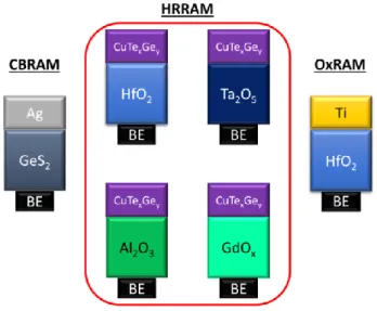
4 2. Technological Details
In this study, various RRAM technologies are investigated. The devices are integrated in
1T1R configuration using 130 nm CMOS transistor as selector. Memory stack is deposited
following bottom electrode (BE)/switching material/top electrode (TE) structure. 5 nm of
amorphous a-HfO2,[26] 3 nm of amorphous a-Al2O3,[29] 4 nm of GdOx,[30] and 10 nm of Ta2O5
were deposited by PVD or ALD on different PVD BEs (titanium nitride-TiN and tungsten W).
20 nm of CuTexGey or 5 nm of Ti deposited by PVD was used as TE for HRRAM and
OxRAM respectively. For the sake of comparison, a typical CBRAM (Ag/GeS2)[11] is
introduced in Figure 1. It has been demonstrated that Te and Ge are not involved in filament
composition.[29] Ge is used to stabilize CuTe layer and to keep it amorphous during
integration process, to prevent any segregation and phase separation. Typically, 10-20% Ge is
used[31,32] in CuTe alloys. Moreover, CuTe bound is polar and can easily be broken in Cu+
and Te- ions. Due to its high formation energy compared to Cu, Te plays no role in the
filament formation. Thus, only Cu ions are mobile under electric field. Consequently, in the
following, HfO2/Cu, Al2O3/Cu, Ta2O5/Cu and GdOx/Cu will refer to HfO2/CuTexGey,
Al2O3/CuTexGey, Ta2O5/ CuTexGey and GdOx/CuTexGey stacks respectively.
3. Hybrid Filament in HRRAM
3.1. ToF-SIMS Measurements
As indicated above, HRRAM is a device where both metallic ions and oxygen vacancies
contribute to switching mechanism. Since a direct microscopic observation of an oxygen
vacancy based filament at nanoscale level is still challenging, here we propose an indirect
method based on Tof-SIMS measurements; a technique based on sputtering a surface with a
focused ion beam and collecting ejected secondary ions. Spectra of copper and oxygen
profiles versus sputtering time in HRS and LRS are presented in Figure 2.a and b for
5
as less Cu in Figure 2.a). An increase of intensity is also observed in the signal incoming from
the Ta2O5 region (indicated as more Cu in Figure 2.a). The copper content shift toward longer
sputtering times corresponds to copper diffusion from the ion source layer (top electrode)
toward the bottom electrode. This copper diffusion is consistent with a CBRAM behavior. On
the other hand, when comparing LRS to HRS of oxygen profile in Figure 2.b, LRS state
profile shows a decrease of oxygen content in the dielectric. Moreover, an increase of oxygen
content is also observed in the CuTe2Ge region. This oxygen content shift corresponds to an
oxygen diffusion toward the surface, leading to oxygen vacancies formation in the oxide as
represented in Figure 2.c. This oxygen diffusion is consistent with OxRAM behavior. It is
worth highlighting that as the ionization yield depends of the atomic environment of the
element, when studying a stack of several layers, some matrix effects can appear at the
interfaces. Moreover, during the sputtering some atoms can be repelled in the sub layers, thus
in the spectra represented in Figure 2.a and b the interfaces positions are roughly estimated.
As observed, both copper and oxygen profiles evolve when an external bias is applied. This
behavior is associated to a hybrid behavior between pure CBRAM, where the filament is
mainly composed of diffused metal and pure OxRAM where the filament is made of a path of
local oxygen deficiencies namely vacancies. This hybrid mechanism is strongly correlated
between vacancies and copper. Oxygen vacancies formed in the oxide weaken the chemical
barrier properties, which eases copper diffusion. Stated differently, copper can easily follow
paths formed by the organization of vacancies in the dielectric, in particular vacancies can be
filled by copper atoms.
3.2. Atomistic Simulations
In order to give insight on microscopic mechanisms that could occur in all our integrated
devices (HfO2/Cu, Ta2O5/Cu, Al2O3/Cu and GdOx/Cu), atomistic simulations were performed.
Combining defect formation enthalpy (∆H) and migration energy barrier (Ea), the most favorable defects that could compose a filament can be extracted. ∆H is the total energy
6
difference between an initial and a final state (introducing a new defect) representing an event
between the oxide and the TE. Ea is the energy needed for a defect to diffuse in the oxide. The
lower these values are, the more favorable the associated event is.
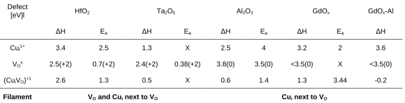
Table 1 summarizes the results. It can be noted, as seen in our calculations, that oxygen vacancy’s formation is required to form the filament. ∆H of copper interstitial next to Oxygen vacancy site (CuiVO) represents the lowest values in all cases validating the hybrid aspect of
the formed filament. On the other hand, ∆H and Ea of VO in HfO2 and Ta2O5 are lower than in
Al2O3 and GdOx. Consequently, two filament features representing two different types of
HRRAM could be identified: HRRAM where only CuiVO defect is moving during memory
operation, and HRRAM where both CuiVO and VO are moving. In HfO2, CuiVO introduction
in the oxide are more favorable (ΔH and Ea lower) than copper interstitial (Cui). Thus,
filament in HfO2 could mainly be composed of VO and CuiVO. In the case of Ta2O5, Cui has a
lower ΔH than VO, nevertheless, it is easier to introduce and remove Cui when it is associated
to VO (ΔH CuiVO =0.5eV). While ΔH of VO is relatively high, it is combined to low migration
energy, making it favorable to diffuse. Thus, in Ta2O5 the switching mechanism involves all
of these studied defects. On the other hand, in Al2O3 and GdOx, CuiVO introduction in the
oxide is the most favorable defect (∆H in the order of 0.6eV vs 3.8eV for VO in Al2O3 and
1.2eV vs 4.1eV for VO in GdOx). Moreover, by introducing aluminum atoms in GdOx
structure, ΔH CuiVO is further reduced leading to a similar behavior as in Al2O3. Although VO
are necessary in HRRAM filament composition, they are either as favorable as CuiVO defect
(as in HfO2) or less favorable (as in Al2O3 and GdOx). In the case of Al2O3 and GdOx, once VO
are created to introduce Cu ions during filament formation, CuiVO are more favorable to be
the core of switching mechanism at the expense of VO. However, in HfO2 andTa2O5 both
CuiVO and VO defects can participate to filament formation and disruption. Indeed in Ta2O5,
ΔH VO is higher than ΔH Cui, but is coupled to a very low migration energy making its
7
between two sites in Al2O3 and HfO2 respectively; Al2O3/Cu and HfO2/Cu being two devices
with different filament features. As we can clearly see, in the case of Al2O3/Cu, (CuiVO) is the
most favorable to be introduced and removed in the filament. On the other hand, in the case of
HfO2, both VO and (CuiVO) are favorable compared to Cui.
4. HRRAM Classification versus Performances
It has been shown that during cycling, non-reversible defect generation gradually degrades the
oxide leading to device failure when the maximum number of cycles is reached.[26,33,34]
Consequently, limiting non-reversible defect generation is a key to improve endurance. Based
on our simulation results, different types of filament are identified. Although VO are required
to favor Cu insertion leading to a hybrid filament, VO can become hard to remove and be
source of defect generation eventually leading to oxide degradation as in GdOx/Cu. In a
material where CuiVO are more favorable than VO, switching filament is richer in Cu.
However, the energy required to remove the small amount of VO is higher than for removing
CuiVO. To remove VO, higher energy should be provided to the oxide, leading to higher defect
generation. Moreover, favoring further CuiVO at the expense of VO as in GdOx-Al/Cu and
Al2O3/Cu leads to a hybrid filament with less VO in its vicinity. In this case, the generation of
non-reversible defects decreases leading to higher endurance. As completely removing VO
from filament formation cannot be considered to decrease defect generation, VO need to be
easily removed to improve endurance. This can be obtained by adjusting CuiVO /VO balance.
In particular, when VO and CuiVO have the same occurrence probability in SET and RESET
operations, they both participate to filament formation and disruption. VO and CuiVO are thus
easily recovered during RESET, leading to low defect generation and good endurance. It can
be noted that if migration energy barrier of both species is high, endurance will be degraded
8
Based on these results, Two groups of HRRAM can be identified as presented in Figure 4: 1)
CuiVO is favored at the expense of VO leading to difficult VO recovery and earlier oxide
degradation (lower endurance). 2) VO as favorable as CuiVO to be removed leads to a VO easy
to recover and thus low defect generation (high endurance). It can be noted that in the case of
VO becoming more favorable than CuiVO, the filament is no longer considered as hybrid and
is mainly composed of VO, leading to OxRAM behavior.
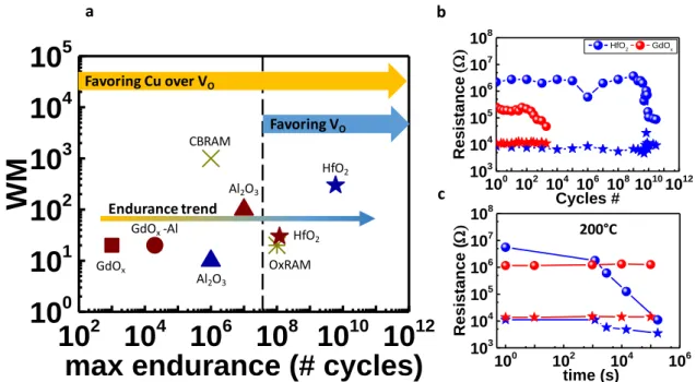
The impact of filament composition on device performances is shown in Figure 5. In order to
compare device performances, three different features could be evaluated: window margin
being the ratio between HRS and LRS, endurance being the maximum of SET/RESET cycles
a cell can reach before final failure (oxide breakdown) and retention representing the
temperature stability over time. These characteristics are interdependent; improving two
features leads to the degradation of the third one. In particular, increasing WM and endurance
degrades retention. Here, we compare the best endurance that could be reached for various
integrated technologies and we correlate the results with filament composition. Figure 5.a
illustrates WM evolution with cycling endurance. Experimental results comply with HRRAM
classification based on atomistic simulations (Figure 4). Red and blue colors represent devices
with TiN and W as bottom electrode respectively. Endurance is lower in Al2O3/Cu and
GdOx/Cu than in HfO2/Cu (details in supplementary material). Adjusting VO and CuiVO
competition in the filament leads to different performances. If VO is as favorable as CuiVO to
be introduced and diffused during SET and RESET (HfO2/Cu), endurance is improved. If VO
is less favorable (Al2O3/Cu and GdOx/Cu), endurance is degraded. In the latter, VO presence,
needed to introduce Cu in the oxide, are less favorable compared to CuiVO. These samples
present an early oxide degradation (lower endurance). Comparing Al2O3 and GdOx where
CuiVO dominates the switching mechanism, GdOx has a lower endurance than Al2O3. This can
be due to a lower defect enthalpy and energy migration barrier (0.6 vs 1.2 eV for ∆H and 1.4 vs 3.44 eV for Ea). As previously seen, by introducing Al in GdOx structure, CuiVO ΔH is
9
further reduced leading to a comparable filament composition as in Al2O3. This is confirmed
in Figure 5.a: by doping GdOx with aluminum, endurance is improved and tends toward
Al2O3. Combining endurance results and atomistic calculations, it appears that Al presence in
the oxide favors Cu insertion next to VO. An OxRAM and a CBRAM are introduced in Figure
5 for comparison sakes.
Consequently, in a material where CuiVO is more favorable than VO, favoring further CuiVO
increases the endurance. In other words, improving Cu insertion leads to a filament easier to
form and disrupt during SET and RESET, leading to a better endurance regardless WM.
Figure 5.b and c represent the comparison between best case and worst case for endurance
and data retention respectively. In figure 5.b, endurance of HfO2/Cu (6.109 cycles) is
compared to GdOx (where only 103 cycles can be reached). On the other hand, in Figure 5.c,
temperature stability of the same devices in Figure 5.b is compared at 200°C. As clearly seen,
the higher the endurance is, the lower the retention is. One should note that endurance
performances are not only related to the hybrid character of the RRAM, but are also linked to
the respective VO, Cu and CuiVO energy costs. Moreover, the highest endurance/WM tradeoff
is due to the use of a tungsten based bottom electrode which favors the RESET due to
tungsten high thermal conductivity favoring thermal dissipation. Thus, the energy needed to
RESET the device is lowered. These conditions favor the cycling capacities of the device at
the expense of the temperature stability as shown in figure S2.b.
To further investigate the difference between the two filament features presented above, we
have studied forming operation with two different polarizations in HfO2/Cuand Al2O3/Cu
(more details in supplementary materials). Figure S.5 represents the time to breakdown tBD
versus forming voltage (Vf). For HfO2/Cu, tBD and Vf are similar in both polarizations. In the
case of Al2O3/Cu, higher forming voltage is observed for short tBD when TE is negatively
polarized preventing Cu insertion in the oxide. HfO2/Cu shows similar switching mechanism
10
polarization. In HfO2, The conductive filament formation with CuiVO or only VO has no
impact on tBD. In Al2O3, as the introduction of copper is more favorable than oxygen
vacancies, its introduction in direct forming eases filament formation and lower forming
voltage.
Consequently, we present a panel of filament composition to be aimed depending on the
targeted application. CBRAMs present high WM while OxRAMs show high endurance and
stable retention. Combining OxRAM and CBRAM in one hybrid HRRAM, performance
compromises could be achieved. Large WM and high endurance are obtained in HfO2/Cu
owing to VO/CuiVO equilibrium in the switching filament. On the other hand, large WM and
stable retention could be achieved due to favoring CuiVO at the expense of VO as in GdOx/Cu
and Al2O3/Cu.
5. Conclusion
In this work, the impact of balancing metal ions and oxygen vacancies in HRRAM filament
on device performances was investigated. Filament composition was studied by first principle
calculations and maximum endurance was identified for different HRRAM. Combining
experimental results and atomistic simulations, we highlighted filament features to improve
endurance characteristics. In particular, we demonstrated that in HRRAM, VO are necessary to
form a Cu-rich filament. The switching mechanism is thus controlled by Cu ions and Oxygen
vacancies. However, two types of filament were put in evidence. Filament where CuiVO are
more favorable to control switching mechanism at the expense of VO (Al2O3 and GdOx)
presents VO hard to be recovered leading to early oxide degradation (low endurance).
Decreasing CuiVO formation enthalpy and diffusion barrier in oxide leads to filament richer in
CuiVO (poorer in VO) and improves endurance. However, VO need to be easily removed
during RESET to further improve endurance. This can be obtained by adjusting CuiVO /VO
11
both defects participate in filament formation and disruption. VO and CuiVO are thus easily
recovered leading to low defect generation (higher endurance as in HfO2/Cu). In summary, we
presented a panel of filament composition, giving insights to choose the most suitable
technology (RRAM resistive layer and electrodes) for a given application with required
specifications.
Acknowledgements
This work has been partially supported by the European 621217 PANACHE project. “Gilbert Sassine and Cécile Nail contributed equally to this work.”
This work was supported by the H2020 WakeMeUp project.
Received: ((will be filled in by the editorial staff)) Revised: ((will be filled in by the editorial staff)) Published online: ((will be filled in by the editorial staff))
References
[1] B. Govoreanu, G. S. Kar, Y-Y. Chen, V. Paraschiv, S. Kubicek, A. Fantini, I. P. Radu,
L. Goux, S. Clima, R. Degraeve, N. Jossart, O. Richard, T. Vandeweyer, K. Seo, P.
Hendrickx, G. Pourtois, H. Bender, L. Altimime, D. J. Wouters, J. A. Kittl, M. Jurczak, 2011
International Electron Devices Meeting, Washington DC, 2011, 31.6.1.
[2] A. C. Torrezan, J. P. Strachan, G. Medeiros-Ribeiro, R. S. Williams, Nanotechnology
2011, 22, 485203.
[3] M-J. Lee, C. B. Lee, D. Lee, S. R. Lee, M. Chang, J. H. Hur, Y-B. Kim, C-J. Kim, D.
H. Seo, S. Seo, U-I. Chung, I-K. Yoo, K. Kim, Nature Materials 2011, 10, 625.
[4] S. Sills, S. Yasuda, J. Strand, A. Calderoni, K. Aratani, A. Johnson, N. Ramaswamy,
2014 Symposium on VLSI Technology (VLSI-Technology): Digest of Technical Papers,
Honolulu, 2014, 1.
[5] J.R. Jameson, P. Blanchard, C. Cheng, J. Dinh, A. Gallo, V. Gopalakrishnan, C.
Gopalan, B. Guichet, S. Hsu, D. Kamalanathan, D. Kim, F. Koushan, M. Kwan, K. Law, D.
Lewis, Y. Ma, V. McCaffrey, S. Park, S. Puthenthermadam, E. Runnion, J. Sanchez, J. Shields,
12
M. Van Buskirk, 2013 IEEE International Electron Devices Meeting, Washington DC, 2013,
30.1.1.
[6] Z. Wei, K. Eriguchi, S. Muraoka, K. Katayama, R. Yasuhara, K. Kawai, Y. Ikeda, M.
Yoshimura, Y. Hayakawa, K. Shimakawa, T. Mikawa, S. Yoneda, 2015 IEEE International
Electron Devices Meeting (IEDM), Washington DC, 2015, 7.7.1.
[7] A. Fantini, L. Goux , R. Degraeve , D.J. Wouters, N. Raghavan , G. Kar , A. Belmonte,
Y.-Y. Chen, B. Govoreanu , M. Jurczak, 2013 5th IEEE International Memory Workshop,
Monterey CA, 2013, 30.
[8] M. Prezioso, F. Merrikh-Bayat, B. D. Hoskins, G. C. Adam, K. K. Likharev, D. B.
Strukov, Nature 2011, 521, 61.
[9] Y. Bai, H. Wu, K. Wang, R. Wu, L. Song, T. Li, J. Wang, Z. Yu, H. Qian, Scientific
Reports 2015, 5, 13785.
[10] I. Valov, R. Waser, J. R. Jameson, M. N Kozicki, Nanotechnology 2011, 22, 289502.
[11] E. Vianello, C. Cagli, G. Molas, E. Souchier, P. Blaise, C. Carabasse, G. Rodriguez, V.
Jousseaume, B. De Salvo, F. Longnos, F. Dahmani, P. Verrier, D. Bretegnier, J. Liebault,
2012 Proceedings of the European Solid-State Device Research Conference (ESSDERC),
Bordeaux, 2012, 278.
[12] S. Pi, M. G. Sadrabadi, J. C. Bardin, Q. Xia, Nature Communication 2015, 6, 7519.
[13] D. B. Strukov, G. S. Snider, D. R. Stewart, R. S. Williams, Nature, 2009, 459, 1154.
[14] J. J. Yang, D. B. Strukov, D. R. Stewart, Nature Nanotechnology, 2013, 8, 13.
[15] G. Sassine, S. La barbera, N. Najjari, M. Minvielle, C. Dubourdieu, F. Alibart, Journal
of Vacuum Science & Technology B, Nanotechnology and Microelectronics: Materials,
Processing, Measurement, and Phenomena, 2016, 34, 012202-1.
[16] T-C. Chang, K-C. Chang, T-M. Tsai, T-J. Chu, S. M. Sze, Materials Today, 2016, 19,
254.
13
[18] G. Sassine, C. Cagli, J. Nodin, G. Molas and E. Nowak, IEEE Journal of the Electron
Devices Society, 2018, 6, 696.
[19] ITRS, “Executive Report,” http://www.itrs2.net/, accessed: 2015. [20] L. Zhu, J. Zhou, Z. Guo, Z. Sun, J Materiomics, 2015, 1, 285.
[21] J. Shang, G. Liu, H. Yang, X. Zhu, X. Chen, H. Tan, B. Hu, L. Pan, W. Xue, R-W. Li,
Adv. Funct. Mater. 2014, 24, 2171.
[22] C. Nail, G. Molas, P. Blaise, B. Sklenard, R. Berthier, M. Bernard, L. Perniola, G.
Ghibaudo, C. Vallée, IEEE Transactions on Electron Devices, 2017, 64, 4479.
[23] R. Waser, R. Dittmann, G. Staikov, Kristof Szot, Adv. Mater. 2009, 21, 2632.
[24] M. Saadi, P. Gonon, C. Vallée, C. Mannequin, H. Grampeix, E. Jalaguier, F. Jomni, A.
Bsiesy, Journal of Applied Physics 2016, 119, 114501.
[25] G. Molas, E. Vianello, F. Dahmani, M. Barci, P. Blaise, J. Guy, A. Toffoli, M.
Bernard, A. Roule, F. Pierre, C. Licitra, B. De Salvo, L. Perniola, 2014 IEEE International
Electron Devices Meeting, San Francisco CA, 2014, 6.1.1.
[26] C. Nail, G. Molas, P. Blaise, G. Piccolboni, B. Sklenard, C. Cagli, M. Bernard, A.
Roule, M. Azzaz, E. Vianello, C. Carabasse, R. Berthier, D. Cooper, C. Pelissier, T. Magis, G.
Ghibaudo, C. Vallée, D. Bedeau, O. Mosendz, B. De Salvo, L. Perniola, 2016 IEEE
International Electron Devices Meeting (IEDM), San Francisco CA, 2016, 4.5.1.
[27] U. Celano, L. Goux, A. Belmonte, K. Opsomer, A. Franquet, A. Schulze, C.
Detavernier, O. Richard, H. Bender, M. Jurczak, W. Vandervorst, Nano Lett. 2014, 14, 2401.
[28] D. S. Jeong, R. Thomas, R. S. Katiyar, J. F. Scott, H. Kohlstedt, A. Petraru, C. S.
Hwang, Rep. Prog. Phys. 2012, 75, 076502.
[29] C. Nail, P. Blaise, G. Molas, M. Bernard, A. Roule, A. Toffoli, L. Perniola, C. Vallée,
14
[30] M. Barci, J. Guy, G.Molas, E. Vianello, A. Toffoli, J. Cluzel, A. Roule, M. Bernard, C.
Sabbione, L. Perniola, B. De Salvo, 2014 IEEE International Reliability Physics Symposium,
Waikoloa HI, 2014, 5E.3.1.
[31] W. Devulder, K. Opsomer, M. Jurczak, L. Goux and C. Detavernier, 2015 IEEE
International Interconnect Technology Conference and 2015 IEEE Materials for Advanced
Metallization Conference (IITC/MAM), Grenoble, 2015, 215.
[32] K. Ohba, S. Yasuda, T. Mizuguchi, K. Aratani, M. Shimuta, A. Kouchiyama,
M.Ogasawara (Sony Semiconductor Solutions Corp), US 13018744, 2011.
[33] S. Balatti, S. Ambrogio, Z.-Q. Wang, S. Sills, A. Calderoni, N. Ramaswamy, D.
Ielmini, 2014 IEEE International Electron Devices Meeting, San Francisco CA, 2014, 14.3.1.
[34] G. Sassine, D. Alfaro Robayo, C. Nail, J.-F. Nodin, J. Coignus, G. Molas, E. Nowak,
2018 IEEE International Memory Workshop (IMW), Kyoto, 2018, 1.
Figure 1. Schematics of RRAM stacks studied in this work. In HRRAM, switching mechanism is controlled by hybrid filaments composed of both Cu and VO species.
15 100 200 300 400 500 101 102 103 Inte nsit y Sputtering time (s) HRS LRS 100 200 300 400 500 10-1 100 101 102 103 Inte nsit y Sputtering time (s) HRS LRS CuTe2Ge/Ti Ta2O5 Less Cu CuTe2Ge/Ti Ta2O5 BE El e c tr ic fi e ld More Cu More O Less O Oxygen ion Copper ion Oxygen vacancy a b c
Figure 2. ToF-SIMS profiles. (a) and (b) copper and oxygen ToF-SIMS profiles in HRS (red lines) and LRS (blue lines) for Ta2O5/Cu memory. In LRS state, Cu intensity in the
CuTe2Ge/Ti region decreases, and increases in Ta2O5 region. Inversely, Oxygen decreases in
Ta2O5 and increases in CuTe2Ge/Ti leading to VO formation in Ta2O5. These profiles illustrate
hybrid composition of the conductive filament in HRRAM. (c) Schematic representation of oxygen and copper ions diffusion under external bias.
0 2 4 6 8 10 -1 0 1 2 3 VO+2 Cui+1 CuiVO
Energy (eV)
Distance (Å)
0 2 4 6 8 10 12 0 1 2 3 4 5Distance (Å)
Energy (eV)
VO Cui+1 CuiVOa
b
Figure 3. Migration barrier of VO, Cui and CuiVO between two sites in (a) Al2O3/Cu and (b)
HfO2/Cu respectively. In Al2O3, diffusion of CuiVO is the most favorable event. On the other
hand, in the case of HfO2, CuiVO and VO are favorable to diffuse.
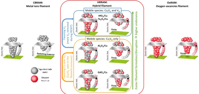
OxRAM: Oxygen vacancies filament CBRAM:
Metal ions filament
HRRAM: Hybrid filament
Mobile species: CuiVOonly
Mobile species: CuiVOand VO
HfO2/Cu Al2O3/Cu GdOx/Cu Easier filamen t forma tion/ dis rup tio n higher end ur ance Fa vori ng Cu o ver V O (Cu/V O ra ti o i n the fil ame n t incr eas es ) Fa vori ng VO (mor e VO remo ved du ri ng RE SET) Ta2O5/Cu
Figure 4. Schematics of filament formation and disruption in different RRAM technologies. CBRAM (left) working principle relies on metal ions, coming from the top electrode,
16
introduction in a switching layer while OxRAM (right) relies on oxygen vacancies formation. Summary of HRRAM filament composition depending on switching materials. Filament is composed of oxygen vacancy (VO) and copper introduced next to VO (CuiVO). Two HRRAM
groups could be distinguished depending on filament composition: 1) CuiVO is favored at the
expense of VO leading to VO hard to be recovered and low endurance (in orange frame). 2) VO
as favorable as CuiVO to be removed leads to a VO easy to recover and thus high endurance
(in blue frame). In the first group, VO is still necessary to form the filament but it is harder to
remove than CuiVO. Group 1 presents thus earlier oxide degradation leading to a low
endurance. However, favoring CuiVO by decreasing its formation enthalpy and migration
energy barrier improves endurance (Al2O3/Cu versus GdOx/Cu). To further improve
endurance, equilibrium between VO and CuiVO is necessary (group 2). Formation enthalpy
and migration energy barrier for both species become of the same order of magnitude leading to filament formation and disruption at a low energy budget.
10
210
410
610
810
1010
1210
010
110
210
310
410
5max endurance (# cycles)
WM
GdOx GdOx-Al CBRAM OxRAM Al2O3 Al2O3 HfO2 HfO2 Favoring Cu over VO Favoring VO Endurance trend 100 102 104 106 103 104 105 106 107 108 Resistance ( ) time (s) 100 102 104 106 10810101012 103 104 105 106 107 108 HfO 2 GdOx Resis tanc e ) Cycles # 200°C a b cFigure 5. (a) Maximum endurance reached for all studied materials. TiN bottom electrode in red and W in blue. Ag/GeS2 CBRAM and HfO2/Ti OxRAM are also presented. The black
dashed line separates the two groups of HRRAM depending on their filament composition. On the left side, decreasing CuiVO formation enthalpy and diffusion barrier in oxide improves
endurance (left arrow). However, on the right side, having VO formation enthalpy and
diffusion barrier of the same order of magnitude as CuiVO avoid early oxide degradation
leading to a better endurance (blue arrow). Endurance trend depending on copper and oxygen vacancies balance in the switching filament composition regardless WM is presented. (b) and (c) comparison between best case and worst case for cycling endurance and data retention respectively.
17
Table 1. Migration energy barrier, Ea, and formation enthalpy, ∆H, between the top electrode
and various oxides extracted from atomistic simulations. Parenthesis represent the charge of the mobile defect.
Defect
[eV]l HfO2 Ta2O5 Al2O3 GdOx GdOx-Al
ΔH Ea ΔH Ea ΔH Ea ΔH Ea ΔH
Cui1+ 3.4 2.5 1.3 X 2.5 4 3.2 2 3.6
VOx 2.5(+2) 0.7(+2) 2.4(+2) 0.38(+2) 3.8(0) 3.5(0) <3.5(0) X <3.5(0)
(CuiVO)+1 2.6 1.3 0.5 X 0.6 1.4 1.3 3.44 -0.2
18
Copyright WILEY-VCH Verlag GmbH & Co. KGaA, 69469 Weinheim, Germany, 2016.
Supporting Information
Title Hybrid-RRAM Towards Next Generation of Non-volatile Memory: Coupling of Oxygen Vacancies and Metal Ions
Author(s), and Corresponding Author(s)* Gilbert Sassine*, Cécile Nail, Philippe Blaise, Benoit Sklenard, Mathieu Bernard, Rémy Gassilloud, Aurélie Marty, Marc Veillerot, Christophe Vallée, Etienne Nowak, andGabriel Molas*
1. ToF-SIMS Measurements
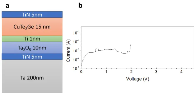
ToF-SIMS measurements were done on Ta2O5/Cu based stack in HRS and LRS. The tested
stack was as follows: Ta (200nm)/TiN (5nm)/Ta2O5 (10nm)/Ti (1nm)/CuTe2Ge (15nm)/TiN
(5nm) as presented in Figure S1.a. For LRS a ramp voltage was applied with a compliance
current fixed at 5x10⁻³ A (figureS1.b). Then a sputter guns with 500eV O2 or Cs were used,
with an ion detection mode with Bi+ and Bi3+ ions at 25keV and a detection of positive ions in
M+, M- and MCs+ modes. ToF-SiMS spectra presented in Figure 2 in the main text show the
diffusion of copper and from CuTe2Ge/Ti toward Ta2O5 during SET operation. On the other
hand, spectra shows diffusion of oxygen from the oxide toward top electrode forming oxygen
vacancies in the vicinity of the dielectric.
2. Electrical Characterization
To study the technology choice impact on endurance, we compare the best endurance that
could be reached for different stacks. First, we compare HfO2/Cu based HRRAM with a
typical HfO2/Ti OxRAM to identify the impact of Cu presence in the switching filament on
device characteristics. Then we identify different type of filament behavior by changing the
switching material in memory stack. Four HRRAM cases are studied (HfO2/Cu, Al2O3/Cu,
19 2.1 HRRAM versus OxRAM
In order to identify Cu contribution in HRRAM, typical HfO2/Ti OxRAM is compared with
HfO2/Cu HRRAM. Figure S2.a and c illustrate the maximum endurance that could be
achieved for both technologies with two different bottom electrodes. In the case of tungsten
BE, HRRAM presents higher maximum endurance as 6.109 cycles could be reached before
degradation, versus 108 in OxRAM. In the case where TiN is used as BE, no clear effect is
noticed. However, retention measurements show that OxRAM presents higher stability over
time than HRRAM. For both BEs no resistance variation is observed after 24h at 200°C for
HfO2/Ti, while HRS failure (resistance drift towards lower values) is obtained in the case of
HRRAM (figure S2.b and d). BE impact on device performance is not treated in this study. In
a previous work [22] a trade-off between WM, endurance and retention can be found in
HRRAM. Increasing WM and endurance in the case of W/HfO2/Cu compared to W/HfO2/Ti
leads to a degraded retention (W BE is chosen as maximum endurance has been reached).
This has been correlated to the energy migration barrier of the species composing the filament.
Decreasing this energy leads to a degraded retention. It can be noted that a correlation with a
typical CBRAM behavior can be made; Ag/GeS2 presents high WM, a relatively high
endurance and a poor retention due to the metallic filament feature [11]. Thus, the low retention
stability of HfO2/Cu could be due to Cu metal ions insertion into filament composition. Cu
presence in the filament could be noticed as well by studying SET behavior in both
technologies.
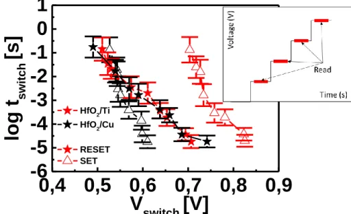
2.2 Copper Impact on Switching Behavior
In the aim of studying copper metal ions contribution in the oxide, a quasi-static voltage ramp
is applied on 1T1R 4kbs memory arrays [18]. This method allows the measurement of
switching voltage and switching time in a memory device. It consists in continuously
increasing the applied voltage at different ramp rate until switching occurs (inset of Figure
20
(HRS to LRS) and RESET (LRS to HRS) respectively. Figure S3 represents switching time in
logarithmic scale versus switching voltage. Based on a previews study[18] it was shown that in
Ramped Voltage Stress the switching time effect is not cumulative. Consequently, the
switching time is computed from the starting of the voltage step where the switching occurs.
It can be noticed that when a positive voltage is applied on the top electrode (TE), a lower
voltage is needed to SET HRRAM compared to OxRAM. However, the same behavior is
observed in RESET for both HRRAM and OXRAM. In SET (positive voltage on the TE),
copper ions insertion in the oxide favors the filament formation. Thus lower energy is
required to SET the HRRAM.
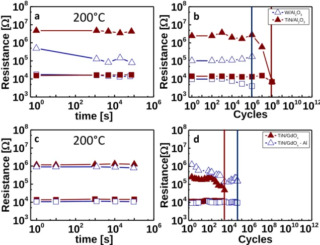
2.3 HRRAM with Stable Retention
As Cu ions contribution to the filament formation was identified in HRRAM, different
behavior are evaluated by changing switching material. In order to show its impact on
endurance, Al2O3 and GdOx known as typical materials for high retention are studied [29.30].
Figure S4.a and c show the retention stability of Al2O3/Cu with two different BEs (TiN and
W) and TiN/GdOx/Cu respectively. There is no resistance variation measured for both
materials at 200◦C. However, as shown in figure S4 b and d, where the best case of endurance
are presented, Al2O3 and GdOx show lower cycling endurance than HfO2/Cu regardless of the
chosen WM; 107and 106 cycles are reached in the case of TiN/Al
2O3/Cu (high WM) and
W/Al2O3/Cu (low WM) respectively. In the case of GdOx/Cu the maximum cycling endurance
we could attain is at the order of 103. Trying to reach Al
2O3 endurance characteristics, GdOx
has been doped with Aluminum (Al). An improvement in cycling endurance is noticed in
GdOx-Al/Cu compared to GdOx/Cu as shown in figure S4 d. Figure S4 c shows no resistance
variation at 200◦C. In conclusion, regardless the chosen WM, Al2O3 and GdOx cannot reach
HfO2/Cu performance in terms of endurance.
21
In this part, forming is studied in HfO2/Cu and Al2O3/Cu HRRAM. Two different
polarizations are applied using the quasi-static method presented above: direct forming where
the forming voltage is applied on the top electrode and reverse forming where the forming
voltage is applied on the bottom electrode. Direct forming implies Copper (Cu) and oxygen
vacancies (VO) formation in the vicinity of the oxide while in reverse forming, as Cu is
positively polarized, its introduction in the oxide is thus not possible. In this case, only VO
formation is considered.In this study, Figure S5 represents the time to breakdown tBD vs
Vswitch for direct and reverse forming. For HfO2/Cu, tBD and Vswitch are similar in direct and
reverse forming. In the case of Al2O3/Cu, higher reverse forming voltage is observed for short
tBD. HfO2/Cu shows similar switching mechanism in both polarizations while Al2O3/Cu
exposes different working principle depending on polarization. In HfO2/Cu, as VO are as
favorable as CuiVO, no real impact of copper insertion on oxide breakdown is observed; same
behavior is noticed in direct and reverse forming. However, in the case of Al2O3, where
CuiVO are more favorable than VO, the filament formation requires lower voltage in direct
forming where CuiVO dominates the switching mechanism compared to reverse forming
where only VO controls the switching.
Ta 200nm
TiN 5nm
Ta
2O
510nm
Ti 1nm
CuTe
2Ge 15 nm
TiN 5nm
a
b
Figure S1. (a) studied stack in ToF-SIMS. (b) Current voltage characteristic of the studied device during SET operation.
22
10
010
210
410
610
310
410
510
610
710
8 OxRAM HRRAMResistance
[
]
time [s]
10
010
210
410
610
810
1010
1210
310
410
510
610
710
8Resis
tanc
e
[
]
Cycles
10
010
210
410
610
310
410
510
610
710
8Resis
tanc
e
[
]
time [s]
10
010
210
410
610
810
1010
1210
310
410
510
610
710
8Resis
tanc
e
[
]
Cycles
a
b
c
d
200°C
200°C
Figure S2. (a) Endurance and retention (at 200°C) measurement for (a), (b) W/HfO2/Cu and
W/HfO2/Ti and (c), (d) TiN/HfO2/Cu and TiN/HfO2/Ti. In (a) and (c) lines designates the
maximum number of cycles reached before filament degradation. In W/HfO2/Cu 6 109 are
reached versus 108 for W/HfO2/Ti (a). As for TiN bottom electrodes (c), 108 could be reached
for both OXRAM and HRRAM. 24 hours stability is reached for OxRAM (W and TiN BE) while HRS failure is clearly observed in HRRAM (b) and (d).
0,4 0,5 0,6 0,7 0,8 0,9
-6
-5
-4
-3
-2
-1
0
1
log
t
sw itc h[s]
V
switch[V]
HfO2/Ti HfO2/Cu RESET SET23
10
010
210
410
610
810
1010
1210
310
410
510
610
710
8 W/Al 2O3 TiN/Al2O3Resistance
[
]
Cycles
10
010
210
410
610
810
1010
1210
310
410
510
610
710
8 TiN/GdO x TiN/GdOx - AlResitance
[
]
Cycles
10
010
210
410
610
310
410
510
610
710
8Resis
tanc
e
[
]
time [s]
10
010
210
410
610
310
410
510
610
710
8Resis
tanc
e
[
]
time [s]
200°C
200°C
a
b
c
d
Figure S4. Retention at 200°C and endurance measurement for (a), (b) W/Al2O3/Cu and
TiN/Al2O3/Cu. and (c), (d) TiN/GdOx/Cu and TiN/GdOx-Al/Cu. 24 hours stability is reached
for all tested HRRAM devices (a) and (c). Lines designates the maximum number of cycles reached before filament degradation. In W/Al2O3/Cu 106 cycles are reached versus 107 cycles
for TiN/Al2O3/Cu (b). As for GdOx (d), 103 cycles are reached, whereas up to 5 104 cycles are
obtained after Al doping.
2,5
3,0 3,5
4,0 4,5
5,0
-6
-5
-4
-3
-2
-1
0
1
Al2O3 HfO2 reverse forming direct forminglog
t
BD[s]
V
switch[V]
Figure S5. (a) tBD versus forming voltage in direct and reverse polarity for HfO2/Cu and