HAL Id: hal-03031816
https://hal.archives-ouvertes.fr/hal-03031816
Submitted on 30 Nov 2020
HAL is a multi-disciplinary open access
archive for the deposit and dissemination of
sci-entific research documents, whether they are
pub-lished or not. The documents may come from
teaching and research institutions in France or
abroad, or from public or private research centers.
L’archive ouverte pluridisciplinaire HAL, est
destinée au dépôt et à la diffusion de documents
scientifiques de niveau recherche, publiés ou non,
émanant des établissements d’enseignement et de
recherche français ou étrangers, des laboratoires
publics ou privés.
Effect of surface roughness on the anomalous Hall effect
in Fe thin films
Qiang Zhang, Dongxing Zheng, Yan Wen, Yuelei Zhao, Wenbo Mi, Aurelien
Manchon, Olivier Boulle, Xixiang Zhang
To cite this version:
Qiang Zhang, Dongxing Zheng, Yan Wen, Yuelei Zhao, Wenbo Mi, et al.. Effect of surface roughness
on the anomalous Hall effect in Fe thin films. Physical Review B, American Physical Society, 2020,
�10.1103/PhysRevB.00.004400�. �hal-03031816�
Effect of surface roughness on the anomalous Hall effect in Fe thin films
2
Qiang Zhang ,1,*Dongxing Zheng,1Yan Wen,1Yuelei Zhao,1Wenbo Mi ,2Aurelien Manchon,1
Olivier Boulle,3and Xixiang Zhang 1,†
3 4
1King Abdullah University of Science and Technology (KAUST), Physical Science and Engineering Division (PSE),
Thuwal 23955-6900, Saudi Arabia
5 6
2Tianjin Key Laboratory of Low Dimensional Materials Physics and Preparation Technology, School of Science,
Tianjin University, Tianjin 300354, China
7 8
3IRIG-SPINTEC, CNRS, CEA, Grenoble INP, Université Grenoble Alpes, 38000 Grenoble, France
9
(Received 4 September 2019; revised manuscript received 13 March 2020; accepted 17 March 2020; published xxxxxx)
12 13
Surface roughness plays an important role on the magnetotransport properties of thin films, especially in ultrathin films. In this work, we prepared Fe thin films with various surface roughness by using different seed layers and studied the electrical transport and anomalous Hall effect. By tuning surface roughness scattering, the longitudinal resistivity (ρxx) measured at 5 K increases by one order of magnitude and the corresponding
anomalous Hall resistivity (ρAHE) increases by three times with increasing roughness. The intrinsic,
skew-scattering, and side-jump contributions to ρAHEwere separated from our data. The anomalous Hall angle depends
on the surface roughness, which may be of importance to the material engineering for achieving large spin Hall angle. 14 15 16 17 18 19 20 21 DOI:10.1103/PhysRevB.00.004400 22 I. INTRODUCTION 23
Anomalous Hall effect (AHE) in magnetic materials, since 24
its discovery [1], has been extensively studied for the fun-25
damental interests and potential applications. It is generally 26
accepted that the intrinsic and extrinsic mechanisms, both 27
of which are related to spin-orbit coupling, are responsible 28
for the AHE. Microscopically, the intrinsic mechanism [2–5], 29
independent of impurity scattering, originates from the Berry 30
phase of the occupied Bloch states. The extrinsic mechanism 31
arising from impurity scattering includes two contributions, 32
skew scattering [6], and side jump [7]. Skew scattering comes 33
from the asymmetric scattering at impurity sites and side jump 34
emerges from transverse displacement of the wave function by 35
impurity scattering. 36
Theories also suggested the scaling relations [2,6,7] be-37
tween anomalous Hall resistivity (ρAHE) and longitudinal
re-38
sistivity (ρxx) for each mechanism: ρAHE ∝ ρxx2 for both the in-39
trinsic and extrinsic side-jump mechanism, while ρAHE ∝ ρxx
40
for extrinsic skew-scattering mechanism. The scaling law is 41
usually applied to experimental data to explore the underlying 42
mechanisms. Experimentally, both the ρAHE and ρxx should
43
be tuned in some range to give a reliable scaling relation. To 44
this end, one option is varying the film thickness where the 45
ρxxcould be changed by surface scattering [8–12]. Films with 46
different thickness are also eligible to study the surface scat-47
tering effect on the AHE [13,14]. However, surface scattering 48
strength/potential is not only related to the thickness of the 49
*Current address: Core Technology Platforms, New York
Univer-sity Abu Dhabi, P.O. Box 129188, Abu Dhabi, United Arab Emirates.
†Corresponding author: [email protected]
films but also to the surface roughness, especially in ultrathin 50 films. Furthermore, the studies of spintronic topics of spin 51 orbital torque (SOT), interfacial Dzyaloshinskii-Moriya Inter- 52 action (DMI) and perpendicular magnetic anisotropy (PMA) 53 are all involved with ultrathin films. The surface/interface 54 roughness may play an important role on these topics (see 55 Sec. 1 in Ref. [15]), which has been omitted in these studies. 56 Few theoretical studies have suggested that surface roughness 57 scattering could lead to a completely different scaling relation 58 between ρAHE and ρxx for spin Hall effect [16] or enhance 59 the spin Hall angle [17] in ultrathin films. However, an 60 experimental study of surface roughness effect on magneto- 61 transport properties, particularly AHE, in thin films is still 62
lacking. 63
In this study, we report the surface roughness effect on the 64 AHE in Fe thin films (see the definition of surface roughness 65 in Sec. 2 of Ref. [15]). The surface roughness could be 66 affected by several factors in deposited thin films: seed layer 67 on substrate [18], substrate temperature [19], thickness of 68 deposited films [20], argon pressure during deposition [21], 69 etc. To study the surface roughness effect, we must keep all 70 other parameters of the samples the same and only vary the 71 surface roughness. Therefore, we cannot use different deposi- 72 tion temperature or thickness of films since it will change the 73 microstructure or surface scattering strength. We then used 74 different materials of seed layers to tune the surface rough- 75 ness. This idea is utilizing the wetting property of materials, 76 which is similar to the chemistry concept of the wettability 77 of liquid contacting with a solid surface. By this method, we 78 may most probably be able to keep all parameters (such as 79 microstructure, thickness, etc.) the same but the roughness. 80 It is, therefore, feasible to the study of the impact of surface 81
QIANG ZHANG et al. PHYSICAL REVIEW B 00, 004400 (2020)
II. EXPERIMENTAL METHODS
83
The samples were deposited on substrates of oxidized 84
silicon wafers by sputtering system (Rotaris, Singulus). The 85
structure of the films is, from the substrate side, seed layer 86
(0.2 nm)/Fe (5 nm)/SiO2 (5 nm) with different seed layers
87
(Ta, Ir20Mn80, MgO, Ru, Co60Fe20B20, SiO2, Co, Ni, CuN,
88
Cu). The samples were deposited, at room temperature, with 89
the base pressure lower than 8.0 × 10⁻⁹mbar and the process
90
pressure 3 × 10⁻³mbar. The deposition of SiO2 with 5 nm
91
thickness as a top layer for each sample is to prevent sam-92
ple oxidization. The surface roughness of the samples was 93
characterized by atomic force microscope (AFM) (Dimen-94
sion Icon, Bruker). The cross-sections of the samples were 95
imaged by high-resolution transmission electron microscopy 96
(HRTEM) (Titan 80–300, FEI). Grazing incidence diffraction 97
(GID) measurements were carried out using x-ray diffraction 98
(XRD) (D8 ADVANCE DAVINCI design, Bruker) with Cu 99
Kαradiation. The longitudinal resistivity and Hall resistivity 100
were measured by a physical property measurement system 101
(Dynacool 14T, Quantum Design). The Hall-bar samples with 102
dimensions 1000 µm (length) × 50 µm (width) were pat-103
terned by photolithography and ion beam etching for trans-104
port measurements. A five-contact geometry was used for 105
simultaneously measuring the Hall resistivity and longitudi-106
nal resistivity on the same piece of sample. A DC constant 107
current of 20 µA was applied during all electrical transport 108
measurements. The sample electrodes were connected to the 109
sample holder of the PPMS by wire bonder using aluminum 110
wires. 111
III. RESULTS AND DISCUSSION
112
A. Structural characterizations
113
To demonstrate the surface roughness of the Fe layers, 114
the samples was imaged by AFM. Due to the existence of 115
the protection layers, the AFM images only give the surface 116
roughness of the SiO2 layers, which could indirectly reflect
117
the surface roughness of Fe layers. As seen in Fig. S1 and 118
the corresponding analysis in Supplemental Material [15], 119
the roughness of sample Cu/Fe is higher than that of sample 120
Ta/Fe, which indicates the larger roughness of Fe layer in 121
Cu/Fe sample than that in Ta/Fe sample. To directly show the 122
surface roughness of the Fe layers, we characterized the cross-123
sections of the samples by HRTEM. The TEM specimens with 124
cross-sections were extracted from the macroscopic samples 125
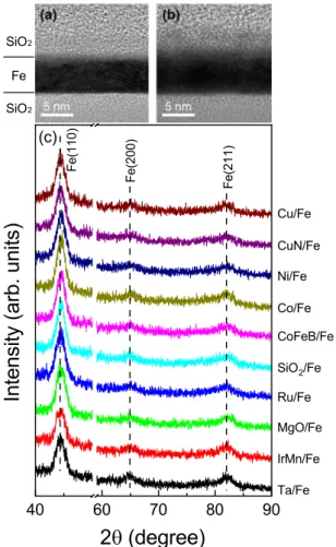
using focus ion beam (FIB). Figures1(a)and1(b)show the 126
bright-field HRTEM images of the cross-sections of selected 127
samples, Ta/Fe and Cu/Fe, respectively. The dark areas could 128
be easily identified as Fe layers and the thickness is consistent 129
with the preset value of 5 nm. The bottom SiO2 layers are
130
from the thermally oxidized wafer substrates and the top SiO2
131
layers were deposited by sputtering. The 0.2-nm-thick seed 132
layers, Ta or Cu, between Fe and substrates can hardly be 133
identified. As seen in Figs.1(a)and1(b), the thickness of Fe 134
layers is identical to each other, but the interfaces between top 135
SiO2and Fe layers is much rougher in sample Cu/Fe than that
136
in sample Ta/Fe. The seed layers indeed play an important role 137
on the surface roughness of Fe layers due to the variation of 138
wetting property of Fe on the seed layer and (maybe) also of 139
FIG. 1. HRTEM images of cross-sections of the samples (a) Ta/Fe and (b) Cu/Fe. (c) GID spectra for all samples.
the wetting property of seed layers on SiO2. To examine the 140 microstructures of the samples, GID measurements were run 141 for all samples with grazing incident angle of 0.5°. Figure1(c) 142 shows the GID spectra for all samples. The diffraction peaks 143 (110), (200), and (211) of bcc-Fe could be identified. For each 144 peak, the intensity and full width at half maximum (FWHM) 145 are quite identical for all samples, indicating that the samples 146
have similar crystallinity. 147
B. Longitudinal resistivity 148 To understand the surface roughness effect on the electrical 149 transport properties, we measured the temperature-dependent 150 longitudinal resistivity of the samples at zero magnetic field 151 in the temperature range of 5–300 K. Figure 2(a) presents 152 the ρxx− T curves for all samples. It is evident that all 153 curves show an overall metallic behavior, i.e., all samples have 154 positive temperature coefficient of resistivity (TCR, dρxx/dT) 155 at high temperatures. The upturn of ρxx(T ) curves below very 156 low temperature have a negative TCR and could be ascribed 157 to an electrical conduction dominated by two-dimensional 158 weak localization effect which was verified by the linear 159 dependence of ρxx on lnT (see Fig. S2 in Ref. [15]). The 160 most important feature is that the ρxx(T ) curves shift to higher 161 values over the whole temperature range from sample Ta/Fe 162 to Cu/Fe, although the thickness of Fe layers is identical 163
FIG. 2. (a) Temperature-dependent longitudinal resistivity (ρxx)
curves for all samples. (b) Normalized ρxx(T )/ρxx(300 K) ∼ T
curves for all samples.
(5 nm) for all samples. At 5 K, the ρxxincreases by one order 164
of magnitude from sample Ta/Fe to Cu/Fe. The insulating 165
seed layers don’t contribute any resistance to the measurement 166
results. For metal or alloy seed layers with thickness of 167
0.2 nm, they would have much higher resistance than that 168
of Fe layers due to the size effect [11]. Furthermore, the 169
0.2-nm-thick seed layers can hardly be continuous layers 170
but rather discontinuous clusters. Therefore, the seed layers 171
have negligible contribution to the longitudinal resistivity of 172
the samples. We ascribe the large resistivity variation of the 173
samples to the surface roughness which could be regarded as 174
effective impurity. At locations where the thickness is thinner 175
than the average thickness, the mean free path of electrons 176
was reduced, which increases the resistivity significantly even 177
though the average thickness is the same. To better under-178
stand the surface roughness scattering effect on electrical 179
resistivity, we replotted the data in Fig.2(a) in the form of 180
ρxx(T )/ρxx(300 K) − T , as shown in Fig.2(b). The resistivity 181
ratio, ρxx(T )/ρxx(300 K), increases from sample Ta/Fe to 182
Cu/Fe, indicating larger scattering effect [22]. Tmin, defined as
183
the temperature where the ρxx is minimum in each ρxx− T 184
curve, increases from sample Ta/Fe to Cu/Fe as shown in 185
Fig. S3 in Ref. [15], clearly demonstrating more frequent scat-186
tering. Overall, the surface roughness of the samples plays an 187
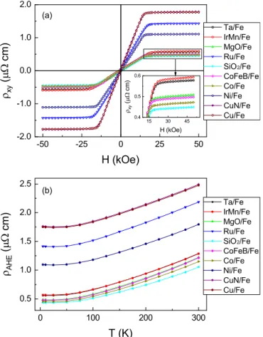
FIG. 3. (a) Field-dependent Hall resistivity (ρxy) of all samples
measured at 5 K. (b) Temperature-dependent anomalous Hall resis-tivity (ρAHE) for all samples.
important role in longitudinal resistivity although the samples 188 have the same thickness and microstructure. 189
C. Anomalous Hall resistivity 190 Since we have observed that the surface roughness signif- 191 icantly affects the longitudinal resistivity, we now turn our 192 attention to that how the surface roughness affects the anoma- 193 lous Hall resistivity. The Hall resistivity (ρxy) for all samples 194 was measured with a magnetic field applied perpendicularly to 195 the plane of the films in a range of −50 kOe ! H ! 50 kOe 196 and at temperatures ranging from 5 to 300 K. Figure 3(a) 197 shows the field-dependent Hall resistivity of all samples mea- 198 sured at 5 K. As it is seen, the Hall resistivity follows a linear 199 and strong dependence on applied magnetic field up to the 200 magnetic saturation field (Hsat). At field higher than Hsat, the 201 Hall resistivity shows a linear and much weaker dependence 202 on applied magnetic field. Zero coercivity has been observed 203 in these curves. These are typical behaviors for magnetic thin 204 films having in-plane magnetization at zero field. At high 205 magnetic fields, the weakly field-dependent Hall resistivity 206 should be ascribed to the ordinary Hall effect and the slight 207 change of the AHE due to the improved alignment of spins. 208 At this stage, the field-forced alignment of spins is a result 209 of thermal agitation (except at 0 K) and nonferromagnetic 210 coupling at Fe layer surface or defects inside Fe layers. Since 211 Fe has high Curie temperature (1043 K), the thermal agitation 212
QIANG ZHANG et al. PHYSICAL REVIEW B 00, 004400 (2020)
FIG. 4. (a) Anomalous Hall resistivity (ρAHE0) vs longitudinal resistivity (ρxx0) at 5 K. The solid line is a guide to eyes. (b) Intrinsic
anomalous Hall conductivity (b) as a function of ρxx0. The inset shows the linear dependence of b on σxx0. (c) Extrinsic anomalous Hall
resistivity as a function of ρxx0. The solid line is a fitting curve by Eq. (7). The same set of data shown in the inset was fitted by Eq. (3).
(d) The anomalous Hall angle (ρAHE0/ρxx0) at 5 K vs ρxx0.
effect could be ignored. For the nonultrathin Fe layers, the 213
nonferromagnetic coupled spins have minor contribution to 214
the Hall resistivity. Therefore, in these samples, the magnitude 215
of anomalous Hall resistivity with negligible error could be 216
obtained by extrapolating the linear part to zero field. 217
As seen in Fig. 3(a), the Hall resistivity increased by 218
four time from the lowest value to the highest. To better 219
demonstrate the variation of the anomalous Hall resistivity, 220
we plotted the temperature-dependent ρAHE for all samples
221
in Fig. 3(b). The sign of ρAHE is positive for all samples
222
across the full temperature range, which is consistent with 223
that reported in pure Fe films [9]. The ρAHE− T curve for
224
each sample shows the same tendency as ρxx− T curve. The 225
ρAHEflattens off below 50 K in all samples, indicating that the
226
phonon scattering effect on the AHE could be ignored at low 227
temperatures. The ρAHE slightly increases with temperature
228
decreasing at low temperatures, which may be due to the weak 229
localization effect. The slight changes are very small (less than 230
1%) and we could ignore the weak localization effect on ρAHE
231
in AHE scaling analysis. 232
D. Anomalous Hall effect scaling analysis
233
To study the origin(s) of the AHE in these samples, the 234
conventional scaling relation, 235
ρAHE/ρxx= c + dρxx, (1)
was usually employed, where c is the contribution of skew 236 scattering, d is the contribution of intrinsic mechanism or side 237 jump. This equation includes both the impurity scattering and 238 phonon scattering effect on mechanisms of skew scattering or 239 side jump. Recently, a new scaling relation [9], 240
ρAHE= αρxx0+ βρxx20+ bρxx2, (2) was proposed in Fe thin films, where α represents the con- 241 tribution from the skew-scattering, β and b denote the side- 242 jump and intrinsic anomalous Hall conductivity (AHC), re- 243 spectively. The subscript “0” indicates that the data were 244 obtained at low temperatures where thermal contribution is 245 negligibly small. This scaling relation excluded the contri- 246 bution of phonon scattering to skew scattering or side jump. 247 To demonstrate if the phonon scattering affects the extrinsic 248 mechanisms, we plotted the relations, ρAHE/ρxx∼ ρxx and 249 ρAHE∼ ρxx2, for the data of each sample, as suggested in 250 reference [9], to compare the linearity. We found that the 251 relation ρAHE ∼ ρxx2 shows better linearity for all samples 252 (see Fig. S4 and the corresponding analysis in Ref. [15]). 253 Therefore we could ignore the phonon scattering effect on 254 skew scattering or side jump and use the new scaling, Eq. (2), 255
to analyze our data. 256
To present the roughness effect on both the longitudinal 257 resistivity and anomalous Hall resistivity, we plotted the rela- 258 tion ρAHE0∼ ρxx0, obtained at 5 K, for all samples in Fig.4(a). 259 From sample Ta/Fe to Cu/Fe, the nonmonotonic dependence 260
suggests very complicated roughness scattering effect on the 261
AHE. One may ask if the ρAHE0 could be affected by the
262
saturation magnetization because anomalous Hall resistivity 263
is not only related to the longitudinal resistivity but also the 264
magnetization [23,24]. The saturation magnetization of the 265
samples could be estimated by the magnetic saturation field 266
in Hall resistivity curves, since the samples have in-plane 267
magnetization (demagnetization factor N = 1 in out-of-plane 268
direction), as shown in Fig.3(a). The variation of magnetiza-269
tion has minor effect on the ρAHE0.
270
Since the linear relation, ρAHE ∝ ρxx2, has been observed 271
for each sample, we could extract the intrinsic AHC which 272
is independent of scattering by Eq. (2). The obtained values 273
of b were plotted as a function of ρxx0 in Fig. 4(b). The
274
intrinsic AHC dramatically decreases with ρxx0 increasing,
275
which could be well described by the relation b ∝ 1/ρxx0
276
or b ∝ σxx0. The inset shows the linear dependence of b on
277
σxx0. Because the ρxx0was largely tuned by surface roughness
278
scattering, the relation b ∝ 1/ρxx0 clearly demonstrates the
279
surface roughness effect on intrinsic AHC. In fact, the electri-280
cal transport properties of the samples are largely determined 281
by the areas where the thickness is lower than the aver-282
age thickness. With thickness decreasing, the intrinsic AHC 283
would decrease, which has been reported in Fe ultrathin films 284
[9,12]. For the flattest sample, Ta/Fe, the intrinsic anomalous 285
Hall conductivity is about 746.7 %−1cm−1which is very close
286
to the value obtained by first-principles calculation [5]. 287
The intrinsic anomalous Hall resistivity could be sub-288
tracted from the total anomalous Hall resistivity and then 289
the extrinsic contribution, including skew-scattering and side-290
jump, of anomalous Hall resistivity, 291
ρAHE0(ex)= αρxx0+ βρxx20 (3)
could be obtained. The data of ρAHE0(ex) versus ρxx0 were
292
plotted in Fig.4(c). Obviously, this curve cannot be well fitted 293
by Eq. (3). For the scattering-related transport properties in 294
thin films, both the surface scattering and bulk scattering con-295
tribute. The longitudinal resistivity at 5 K could be expressed 296
as 297
ρxx0= ρxx0(s)+ ρxx0(b). (4)
Accordingly, the scattering-related anomalous Hall resistivity 298
at low temperatures is also expressed as 299
ρAHE0(ex)= ρAHE0(s)+ ρAHE0(b). (5)
The subscripts (s) and (b) denote the contributions from 300
the surface scattering and bulk scattering, respectively. In 301
Fig.4(c), the variation of ρAHE0(ex)and ρxx0is only due to the
302
surface scattering. The bulk scattering contribution, ρAHE0(b)
303
and ρxx0(b) kept constant for these samples. Therefore using
304
expression 305
ρAHE0(s)= αρxx0(s)+ βρxx20(s) (6)
instead of Eq. (3) is more appropriate to describe the behavior 306
in Fig.4(c). If we put Eqs. (4) and (5) into Eq. (6), Eq. (6) 307
could be expressed as 308
ρAHE0(ex)= (α − 2βρxx0(b))ρxx0+ βρxx20
+ !βρ2xx0(b)− αρxx0(b)+ ρAHE0(b)". (7)
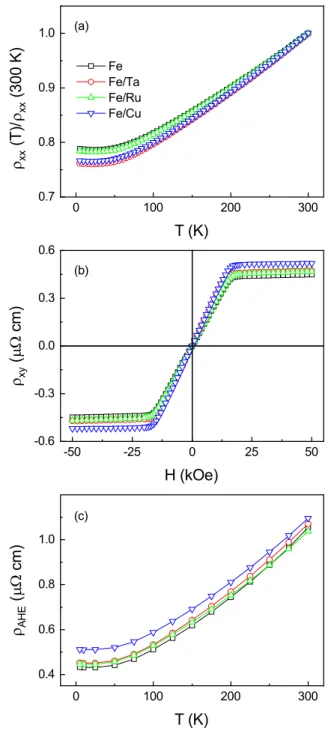
FIG. 5. (a) Normalized ρxx(T )/ρxx(300 K) ∼ T curves for the
samples listed in the legend. The legend is the same in (b) and (c). (b) Field-dependent Hall resistivity measured at 5 K. (c) Temperature-dependent ρAHEfor the samples.
In this equation, ρAHE0(ex) and ρxx0 are variables and other 309 parameters are all constants. Using Eq. (7) to fit the 310 curve in Fig. 4(c), we can extract the parameters as β = 311 40.4 %−1cm−1 and α − 2βρxx0(b)= −1.59 × 10⁻². Since 312
Eq. (7) is overparametrized, we cannot get the exact value 313 of α but roughly estimate it. For the sample Ta/Fe, ρxx0= 314 2.58×10⁻⁵%cm and ρxx0(b)should be lower than that. There- 315
fore 2βρxx0(b)≪ 1.59 × 10⁻² and then α ≈ −1.59 × 10⁻². 316 Comparing the ρAHE0(ex)and intrinsic anomalous Hall resistiv- 317 ity, the intrinsic one dominates the anomalous Hall resistivity 318
QIANG ZHANG et al. PHYSICAL REVIEW B 00, 004400 (2020)
Anomalous Hall angle characterized by the ratio of 320
ρAHE/ρxx was also studied for these samples with various 321
surface roughness. Figure 4(d)shows the data, measured at 322
5 K, of ρAHE0/ρxx0versus ρxx0. The ρAHE0/ρxx0decreases with
323
ρxx0increases at lower ρxx0and increases with ρxx0at higher
324
ρxx0. Overall, the largest anomalous Hall angle was achieved
325
in sample Ta/Fe, which is the flattest sample with minimum 326
surface roughness. This finding opens a promising avenue 327
for achieving large spin Hall angle by surface roughness 328
engineering in heavy metals. 329
The previous theoretical study on spin Hall effect has 330
proposed surface roughness enhanced spin Hall angle in Cu 331
and Al [17]. In this study, only surface roughness scattering 332
related extrinsic mechanisms were considered and intrinsic 333
mechanism was not discussed. It turns out that the side-jump 334
mechanism contributes to the surface roughness induced spin 335
Hall effect but screw scattering does not. In our work, both 336
screw scattering and side jump contribute to the extrinsic 337
mechanisms which may partially come from the surface 338
scattering, because the roughness scattering and effective 339
surface scattering cannot be separated experimentally. With 340
the surface roughness increases, the side jump contributed 341
anomalous Hall angle (βρxx0(s)) increases, which is consistent
342
with the results of the theoretical work [17]. 343
Since we observed the variation of anomalous Hall resis-344
tivity for these samples with different seed layers, one may 345
quest if the variation is caused by the interfacial spin-orbital 346
coupling [25,26] or interfacial modification [27] other than 347
the surface roughness. We then prepared several samples 348
with the same roughness but different interfacial spin-orbital 349
coupling. The sample structure is, from the substrate side, 350
Fe(5 nm)/cover layer(0.2 nm)/SiO2(5 nm) with different cover
351
layers (Ta, Ru, Cu). The sample, Fe(5 nm)/SiO2(5 nm),
352
without metal cover layer was also prepared for comparison. 353
The same substrate material (SiO2) lead to the same
rough-354
ness of Fe layers and different cover layers provide differ-355
ent interfacial spin-orbital coupling. We then measured the 356
temperature-dependent longitudinal resistivity and anomalous 357
Hall resistivity. Figure5(a)shows the normalized longitudinal 358 resistivity curves for the four samples. As seen, the resistivity 359 ratio, ρxx(T )/ρxx(300 K), is quite identical, which indicates 360 the similar extent of surface scattering in these samples. Fig- 361 ure5(b)presents the field-dependent Hall resistivity measured 362 at 5 K for the four samples. The four curves show similar 363 behaviors and Hall resistivity. The values of ρAHE, extracted 364 from the Hall resistivity curves at different temperatures, were 365 presented in Fig. 5(c). The ρAHE gives identical values at 366 each temperature for different samples, which indicates that 367 the various interfacial spin-orbital coupling cannot explain the 368 large difference of ρAHEin Fig.3(b). 369
IV. CONCLUSIONS 370 We prepared Fe thin films with the same thickness but 371 various surface roughness by using different materials of seed 372 layers. The microstructure and magneto-transport properties 373 were studied systematically. The samples show similar crys- 374 tallinity as seen in GID patterns and distinct surface roughness 375 confirmed by TEM images of cross-sections. The magnitude 376 of longitudinal resistivity measured at 5 K increases by one 377 order from sample Ta/Fe to Cu/Fe. The anomalous Hall 378 resistivity at 5 K vary with different roughness and shows 379 nonmonotonic dependence on ρxx0. The intrinsic contribution 380 dominated the anomalous Hall resistivity and shows linear 381 dependence on the longitudinal conductivity at 5 K. The 382 anomalous Hall angle depends on the surface roughness, 383 which provides an alternative to achieve large spin Hall effect 384
experimentally. 385
ACKNOWLEDGMENTS 386 The research reported in this publication was supported 387 by funding from King Abdullah University of Science and 388 Technology (KAUST), Office of Sponsored Research (OSR) 389 under Award No.CRF-2017-3427-CRG6. Q.Z. acknowledge 390 the financial support by KAUST sensor project (REP/1/2708- 391
01). 392
[1] E. H. Hall,Philos. Mag. 12,157(1881).
[2] R. Karplus and J. M. Luttinger,Phys. Rev. 95,1154(1954). [3] J. W. Ye, Y. B. Kim, A. J. Millis, B. I. Shraiman, P. Majumdar,
and Z. Tesanovic,Phys. Rev. Lett. 83,3737(1999).
[4] T. Jungwirth, Qian Niu, and A. H. MacDonald,Phys. Rev. Lett. 88,207208(2002).
[5] Y. G. Yao, L. Kleinman, A. H. MacDonald, J. Sinova, T. Jungwirth, D. S. Wang, E. G. Wang, and Q. Niu,Phys. Rev. Lett. 92,037204(2004).
[6] J. Smit,Physica 21,877(1955);24,39(1958). [7] L. Berger,Phys. Rev. B 2,4559(1970).
[8] S. Sangiao, L. Morellon, G. Simon, J. M. De Teresa, J. A. Pardo, J. Arbiol, and M. R. Ibarra,Phys. Rev. B 79,014431(2009). [9] Y. Tian, L. Ye, and X. F. Jin,Phys. Rev. Lett. 103, 087206
(2009).
[10] L. Ye, Y. Tian, X. F. Jin, and D. Xiao, Phys. Rev. B 85,
220403(R)(2012).
[11] D. Z. Hou, Y. F. Li, D. H. Wei, D. Tian, L. Wu, and X. F. Jin,
J. Phys.: Condens. Matter 24,482001(2012).
[12] L. Wu, K. Zhu, D. Yue, Y. Tian, and X. F. Jin,Phys. Rev. B 93,
214418(2016).
[13] Z. B. Guo, W. B. Mi, R. O. Aboljadayel, B. Zhang, Q. Zhang, P. G. Barba, A. Manchon, and X. X. Zhang,Phys. Rev. B 86,
104433(2012).
[14] D. Rosenblatt, M. Karpovski, and A. Gerber,Appl. Phys. Lett. 96,022512(2010).
[15] See Supplemental Material athttp://link.aps.org/supplemental/ 10.1103/PhysRevB.xx.xxxxxx for the importance of sur-face/interface roughness in spintronic devices, the definition of surface roughness, AFM analysis of surface roughness for the samples with SiO2protection layers, two-dimensional weak
localization at low temperatures, Tmin∼ ρxx0 relation for all
samples, and comparing the linearity of ρAHE/ρxx∼ ρxx and
ρAHE∼ ρxx2 for all samples.
[16] X. H. Wang, J. Xiao, A. Manchon, and S. Maekawa,
arXiv:1407.8278v1[cond-mat.mes-hall].
[17] L. J. Zhou, V. L. Grigoryan, S. Maekawa, X. H. Wang, and J. Xiao, Phys. Rev. B 91, 045407
(2015).
[18] L. Vj, N. P. Kobayashi, M. S. Islam, W. Wu, P. Chaturvedi, N. X. Fang, S. Y. Wang, and R. S. Williams,Nano Lett. 9,178
(2009).
[19] J. Zhang, C. Liu, Y. H. Shu, and J. Fan,Appl. Surf. Sci. 261,
690(2012).
[20] F. Ruffino, V. Torrisi, G. Marletta, and M. G. Grimaldi,Appl. Phys. A 100,7(2010).
[21] W. F. Shen, D. Mazumdar, X. J. Zou, X. Y. Liu, B. D. Schrag, and G. Xiao, Appl. Phys. Lett. 88, 182508
(2006).
[22] M. Reghu, C. O. Yoon, D. Moses, and A. J. Heeger, in
Hand-book of Conducting Polymers, edited by T. A. Skotheim, R. L. Elsenbaumer, and J. R. Reynolds (Marcel Dekker, New York, 1996), p. 27.
[23] Q. Zhang, P. Li, Y. Wen, X. He, Y. L. Zhao, J. L. Zhang, and X. X. Zhang,J. Phys. D: Appl. Phys. 50,235002(2017). [24] Q. Zhang, Y. Wen, Y. L. Zhao, P. Li, X. He, J. L. Zhang, Y. He,
Y. Peng, R. H. Yu, and X. X. Zhang,J. Phys.: Condens. Matter 29,415802(2017).
[25] X. Wang, J. Xiao, A. Manchon, and S. Maekawa,Phys. Rev. B. 87,081407(R)(2013).
[26] J. Borge, C. Gorini, G. Vignale, and R. Raimondi,Phys. Rev. B 89,245443(2014).
[27] J. L. Xu, Y. F. Li, D. Z. Hou, L. Ye, and X. F. Jin,Appl. Phys. Lett. 102,162401(2013).