HAL Id: cea-01625320
https://hal-cea.archives-ouvertes.fr/cea-01625320
Submitted on 27 Oct 2017
HAL is a multi-disciplinary open access
archive for the deposit and dissemination of
sci-entific research documents, whether they are
pub-lished or not. The documents may come from
teaching and research institutions in France or
abroad, or from public or private research centers.
L’archive ouverte pluridisciplinaire HAL, est
destinée au dépôt et à la diffusion de documents
scientifiques de niveau recherche, publiés ou non,
émanant des établissements d’enseignement et de
recherche français ou étrangers, des laboratoires
publics ou privés.
Software Platform Dedicated for In-Memory Computing
Circuit Evaluation
Maha Kooli, Henri-Pierre Charles, Clément Touzet, Bastien Giraud,
Jean-Philippe Noel
To cite this version:
Maha Kooli, Henri-Pierre Charles, Clément Touzet, Bastien Giraud, Jean-Philippe Noel. Software
Platform Dedicated for In-Memory Computing Circuit Evaluation. RSP’17 (Rapid System
Prototyp-ing), Oct 2017, Séoul, South Korea. �10.1145/3130265.3130322�. �cea-01625320�
Evaluation
Maha Kooli
1, Henri-Pierre Charles
2, Cl´
ement Touzet
1, Bastien Giraud
1, Jean-Philippe No¨
el
11 Univ. Grenoble Alpes, CEA, LETI, F-38000 Grenoble 2Univ. Grenoble Alpes, CEA, LIST, F-38000 Grenoble
ABSTRACT
This paper presents a new software platform, co-developed by research teams with expertises in memory design, and software engineering and compilation aspects, to dimension and evaluate a novel In-Memory Power Aware CompuTing (IMPACT) system for IoT. IMPACT circuit is an emerging memory that promises to save execution time and power con-sumption by embedding computing abilities. The proposed platform permits to manually convert a software applica-tion from convenapplica-tional to IMPACT implementaapplica-tion using vector representation. The two implementations are then compiled on the Low Level Virtual Machine (LLVM) and traced in order to evaluate their performance in terms of timing and energy consumption. The results of emulating image-processing and secure applications on IMPACT system show a significant gain in the execution time and the energy consumption compared to a conventional system with an ARM Cortex®-M7 processor. The execution time can be reduced from 50x to 6145x, depending on the application and the workload size. Furthermore, the gain of the energy consumption is about 12.6x.
CCS CONCEPTS
• Computer systems organization → Heterogeneous (hy-brid) systems;
KEYWORDS
In-memory Computing, Performance, Software Platform, LLVM
ACM Reference Format: Maha Kooli1 , Henri-Pierre Charles2 , Cl´ement Touzet1 , Bastien Giraud1 , Jean-Philippe No¨el1
. 2017. Software Platform Dedicated for In-Memory Computing Circuit Evaluation. In Proceedings of RSP’17, Seoul, Republic of Korea, October 15–20, 2017, 7 pages. https://doi.org/10.1145/3130265.3130322
Permission to make digital or hard copies of all or part of this work for personal or classroom use is granted without fee provided that copies are not made or distributed for profit or commercial advantage and that copies bear this notice and the full citation on the first page. Copyrights for components of this work owned by others than ACM must be honored. Abstracting with credit is permitted. To copy otherwise, or republish, to post on servers or to redistribute to lists, requires prior specific permission and/or a fee. Request permissions from [email protected].
RSP’17, October 15–20, 2017, Seoul, Republic of Korea © 2017 Association for Computing Machinery.
ACM ISBN 978-1-4503-5418-9/17/10. . .$15.00 https://doi.org/10.1145/3130265.3130322
1
INTRODUCTION
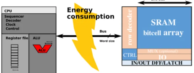
Researchers are nowadays focusing on memory improvement in particular the growing speed gap between memory and computation unit known as the ”memory wall” (Figure 1). One solution to reduce the data movement and the resulting power consumption consists in bringing a part of the memory (i.e., the caches) near to the processor. However, to optimize the data access time the cache sizes are reduced, which re-quires multi cache levels leading to significant increase of the chip area. Therefore, other solutions came up over the years to cover these problems. They can be grouped in the following techniques: Processing-In-Memory, In-Memory-Computing, Logic-In-Memory.
Figure 1: Conventional computing architecture which needs a memory access for all word level com-putation
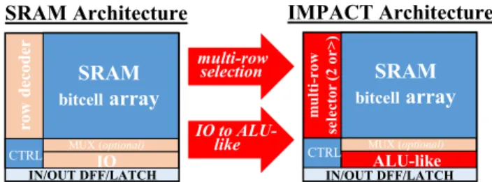
Processing-In-Memory (PIM) is a process based on DRAM, which consists in putting the computation unit next to the memory while keeping the two dissociated [14]. The objec-tive behind bringing the processor near to the memory aims to reduce the time required to access the data inside the memory and therefore the power consumption due to that. This concept has been first introduced in [6] and [17], where the memory and the CPU have been implemented in the same die. In more recent works and with the progress of the 3D technology, researchers propose to design stacks of computation unit (as CPUs [18] or as logic units [7]) next to the memory stack, which permits to create massive data parallelism. Logic-In-Memory is the concept of integrating some computation in the memory. However, it is more used to realize logic operations on a specific memory layer [16] or logic layer dedicated for 3Ds memories [21]. In-Memory Computing (IMC) consists in integrating a part of the com-putation units into the memory boundary (Figure 2), which means that the data do not go out from the memory. This should offer significant gain in the execution time and the
RSP’17, October 15–20, 2017, Seoul, Republic of Korea M. Kooli et al. power consumption. The IMC concept has been applied on
volatile memories [8] and non volatile memories [15] [20] [10]. In [4], the authors present the architecture of in-memory computing applied on the caches. In [9], the authors discuss the different performance gain of this circuit for a face recog-nition algorithm. However, in all these papers, no software platform to simulate the in-memory computing circuit has been presented. All the applications that have been experi-mented to evaluate this concept, are manually analyzed. In this paper, we do not only focus on the architecture of this circuit, but also on the compilation and the programming flow, the point that has not been studied by the existing works. IN/OUT DFF/LATCH IN/OUT DFF/LATCH
SRAM
bitcellarray
MUX (optional) ro w de co de r CTRL IO multi-row selection IO to ALU-like m ul ti -r ow sel ec to r (2 o r>)SRAM
bitcellarray
CTRL MUX (optional)ALU-like
SRAM Architecture
IMPACT Architecture
Figure 2: IMPACT circuit architecture derived from SRAM circuit architecture
In this article, we propose a new software platform that helps to design a new IMPACT circuit in order to quickly investigate different memory layout parameters under the light of real world and high level applications. Thanks to a high level instrumentation trace generator and a trace ana-lyzer able to evaluate the performances. This study permits to help memory designers to select optimum configurations. This paper is based on the work previously published in [5], where the concept of the IMPACT circuit has been first introduced. We present a novel software platform to rapidly prototype the IMPACT system and dimension its circuit. The objective of our research project is to: (i) prove a huge performance improvement in terms of execution time and energy consumption, (ii) help designer to select optimal configurations, and (iii) build a complete IMPACT system going from the software to the hardware layers (Figure 3). The proposed software platform permits to evaluate the execution time and the energy consumption of two software applications first run on a conventional IoT system and then simulated on IMPACT system. The first experimented application is a security one while the second is an image processing application. The results show a timing speed factor varying between 50 and 6145 times, and an energy gain of 12.6 times.
This paper is structured as follows. Section 2 presents a brief description of the IMPACT system. Section 3 introduces the software platform proposed to experiment the IMPACT circuit. Section 4 describes the experimentation. The scenar-ios and the results are then discussed in Section 5. Finally, Section 6 concludes the paper.
8 bit IMPACT Circuit(large ALU-like)1024 byte
CPU
Instruction Set Architecture
Silicon Design Silicon Demonstrator
ALU ALU
Virtual Instruction Set
Compiler Programming Language Software Application So ftware Hardware Technology Layer Progress
Figure 3: General project overview: Evaluating high level applications in order to design suitable memory architectures
2
IMPACT SYSTEM DESCRIPTION
In this section, we describe the concept of IMPACT Circuit. The work published in [5] introduces the concept of IM-PACT circuit. Based on efficient bitcells, it proposes a novel computing circuit using the SRAM architecture to enable in-memory logic and arithmetic operations, as shown in Figure 2. This permits to reduce the data transfer between the memory and the computing units (i.e., ALU). The proposed IMPACT circuit is able to perform the same logic and arithmetic oper-ations as a basic ALU and, therefore enables non-destructive computing and storage in the same unit.
The IMPACT concept is based on an SRAM bitcell array in which multiple rows can be selected at the same time during the same clock cycle for performing in-situ operations between selected rows. The operation type is chosen and con-trolled slice-wise (using a dedicated controller), thus different operations can be performed on different slices of the same ar-ray offering highly-parallel operations. The IMPACT circuit is able to perform different arithmetic and logic operations inside the memory, thus limiting intensive data transfers.
Table 1 provides the description of the logic and arithmetic operations that the IMPACT memory is able to perform. The logic operations are performed in two clock cycles, while the arithmetic operations are performed in three cycles. Based on this timing, we compute the total number of cycles required to run an application on IMPACT system, as it will be presented in Section 5.
2.1
Logic Operations
A native logic operation can be performed when more than one row are selected in a bitcell column. Based on the triple-port SRAM bitcells enabling two read and one write opera-tions per memory access cycle, the read-ports connected to the data stored in the write-port enable to perform NOR operations, while the ones connected to the complementary
Table 1: Arithmetic and Logic Operations enabled by IMPACT System. Operation Type Examples Cycles # Sub-Operations*
LOGIC OR, AND,
INV, XOR, ...
2 cycles Rs -> Ws
ARITHMETIC ADD, SUB,
INC, DEC, ...
3 cycles Rs -> L -> Ws
* Rs: represents the load operation in IMPACT circuit Ws: represents the store operation in IMPACT circuit L: additional cycle for the logic execution
data enable to perform AND operations. Based on this behav-ior, an additional IO circuitry has been designed to perform the rest of valid logic operations with N operands (N cor-responding to the number of selected rows): OR, NAND, EQ (equal) and NEQ (not equal). A selection signal ADD enables to change the nature of the operation on the outputs of the circuitry, which is useful to differentiate addition and subtraction operations.
If only one row is selected, as in a conventional mem-ory, the result on the true read bitline (RBLT), (resp. false read biltine) will be the value of the selected data (resp. complementary data). In this case, the resulting operations performed by the additional IO circuitry are: XOR, NXOR, INV and material implication. This operating mode is used to perform addition, subtraction and word-level compari-son (greater than (GT), lower than (LT) and equal (EQ)) operations.
2.2
Arithmetic Operations
Based on the results of the logic operation of the additional IO circuitry, we implement a ripple-carry adder/subtractor. Only three logic gates are added to perform the operations which are usually implemented only with CMOS logic gates. The selection between the addition and subtraction operation is made by setting the appropriate value on the ADD signal (‘1’ for addition, ‘0’ for subtraction). Increment and decrement operations are performed in the same way by setting the carry to ’1’. All these operations can be performed in one time (e.g. in asynchronous operating mode) or in three equal cycles (e.g. in synchronous operating mode).
Other arithmetic operations are enabled by the IMPACT circuit, such as the comparison operation at word level (GT, LT and EQ). These operations are performed with the same timing constraints as the ADD/SUB operations by adding some logic gates to the additional IO circuitry.
3
SOFTWARE PLATFORM
DESCRIPTION
This paper presents a preliminary software platform to emu-late software applications on IMPACT circuit. The proposed platform will be used to: (i) demonstate a huge performance gain in terms of execution time and energy consumption for IoT, (ii) help designer to select optimal configurations and (iii) build a complete IMPACT system going from the software to the hardware layer.
In order to characterize a new compilation platform for IMPACT circuit, we need to investigate methods and tools to describe the software independently from the target hardware architecture. In fact, at this stage of our research, the Instruc-tion Set Architecture (ISA) of the IMPACT hardware system (smart memory + CPU) is not yet defined and implemented. Therefore, it cannot be used to analyze how the software ap-plications is executed on the IMPACT system. In this paper, we make use of virtualization techniques, in particular LLVM [13], which is a compiler framework that uses virtualization with virtual instruction sets to perform complex analysis of software applications on different architectures. LLVM presents different characteristics that are advantageous for our tool. First, it uses the Intermediate Representation (IR) as a form to represent the code in the compiler, which is similar to an assembly code. The is independent from the source language and the target machine. Furthermore, LLVM allows code to be left for late-compilation from the IR to machine code via the just-in-time compilation. Then, LLVM is able to manipulate very large vectors (e.g., <2048 x i32> a vector of 2048 32-bit integer) and integer with arbitrary bit width varying from 1 bit to 223
−1 (about 8 millions) [3]. The proposed software platform consists in compiling the application implemented in two modes, the conventional and the IMPACT implementations. The IMPACT implementa-tion is based on the LLVM vector representaimplementa-tion of the data, where the word size is dynamically configured. This vector representation interprets the logic/arithmetic operations that are performed in IMPACT circuit. In fact, as explained in Section 2, this circuit is based on SRAM array in which multiple rows can be selected and computed at the same time.
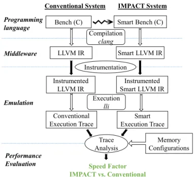
In Figure 4, we provide the flow of the proposed platform going through different system layers. Starting from the C programming language, we implement the given software ap-plication in two versions: (1) the conventional version and (2) the smart version representing the behavior of the IMPACT memory, where the arithmetic/logic operations are computed on data represented as vectors. For example, as shown in Listing 1, a bit-wise between the elements of two byte arrays is implemented, in smart version, as a bit-wise between two vectors of bytes. Each vector corresponds to a line in the smart memory, and the operation is implemented using the LLVM capabilities to manage such operation on large inte-gers/vectors. The output of the application is guaranteed to be the same for the two implementations.
RSP’17, October 15–20, 2017, Seoul, Republic of Korea M. Kooli et al. Bench (C) LLVM IR Speed Factor IMPACT vs. Conventional Smart LLVM IR Smart Bench (C) Programming language Middleware Emulation Performance Evaluation Instrumented LLVM IR Instrumented Smart LLVM IR Instrumentation Conventional Execution Trace Trace Analysis
Conventional System IMPACT System
Compilation clang Execution lli Smart Execution Trace
Manual transformation (similar to OpenCL or CUDA programming model)
Automatic transformation using our implemented tools Automatic generation using existing tools
Memory Configurations
Figure 4: Flow of the proposed platform enabling the generation of execution traces and the performance evaluation of IMPACT system vs. conventional one
The application is then compiled to the middleware LLVM IR code using Clang [2]. The next step consists in executing the application and monitoring the timing. However, LLVM does not provide, at the interpretation mode, information about the executed operation and the exact timing when an instruction is executed. Thus, we propose to instrument the LLVM code by adding instructions to log the executed operation, the address and the size of the operands. This concept has been first introduced in [12]. In this paper, we use this concept to follow the arithmetic/logic operations and the access memory operations (read/write). The instrumented code is therefore executed and traces are recorded for the conventional and the IMPACT executions (Figure 5).
# if SMART
typedef u n s i g n e d char Array
_ _ a t t r i b u t e _ _ (( e x t _ v e c t o r _ t y p e ( LEN ))); # else
typedef u n s i g n e d char Array [ LEN ]; # endif
void C o m p u t e A d d O p ( Array Msg , Array Key ){ Array EncMsg ; # if SMART EncMsg = Msg ^ Key ; # else for ( i = 0; i < LEN ; ++ i ){ EncMsg [ i ] = Msg [ i ]^ Key [ i ]; } # endif }
Listing 1: Conventional vs. IMPACT implementa-tion
The traces resulting from the two executions are analyzed by computing the total number of cycles and the energy consumption. For the conventional execution, the number of cycle and the energy consuption are provided by the selected technology and processor. For the IMPACT execution, we consider the timing information provided in Table 1. The final step consists in computing the speed factor as the ratio be-tween the cycles and energy consumption of the conventional execution and the IMPACT execution.
Conventional ExecutionTrace IMPACT Execution Trace load 8 0x7d640 load 8 0x7d642 add 8 0x7d640 0x7d642 0x7d644 store 8 0x7d644
add 32 0x7ece0 0x7ece8 0x7ecf0 icmp 32 0x7ede0 0x7ede8 0x7edf0 br
smartAdd 512 0x7d640 0x7d240 0x7ce40
x 64
(a)
(b)
Figure 5: (a) Conventional execution trace, (b) IM-PACT execution trace
4
EXPERIMENTATION
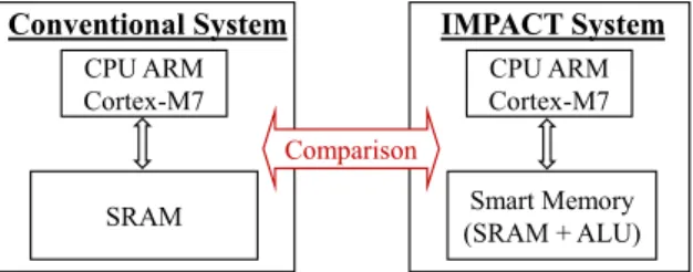
In order to evaluate the IMPACT circuit, we set up a con-ventional system for the sake of refrence. In this paper, we compare the execution time and the energy consumption required to simulate a software application on an IMPACT system to the execution time and the energy consumption required to run the same application on a conventional sys-tem. To have a fair comparison, we set up the same CPU for both systems. In particular, we use an ARM Cortex®-M7 processor, which is the most recent and highest performance member of the energy-efficient ARM Cortex-M series [1]. As shown in Figure 6, the conventional system is composed of a CPU (without cache to represent IoT devices) and an SRAM, while the IMPACT system is composed of a CPU and a smart memory based on SRAM.
To compute the timing of the conventional execution, we consider that the read/write operations take only one cycle to access data in the memory, and that the arithmetic/logic
Conventional System IMPACT System
CPU ARM
Cortex-M7 CPU ARM Cortex-M7
SRAM (SRAM + ALU)Smart Memory
Comparison
Figure 6: Experimental platform
operations take one cycle to be executed in the CPU. In fact, for this paper, we are considering the optimal case for the conventional system, where the chip frequency is equal to the memory frequency.
To compute the timing of the IMPACT execution, we use the information provided in Table 1 about the number of cycle required by each operation.
Then to evaluate the energy consumed by the applica-tion, we consider the energy consumed by each smart and conventional operation (read, write, arithmetic/logic). These information are provided thanks to measurements internally done in our research group.
Having the number of cycles and the energy consumed in pJ for each execution, we compute the gain of the IMPACT system comparing the conventional system. It is important to mention that for this paper, we evaluate the execution time and energy consumption only for the function that is per-forming the arithmetic/logic data computation. In addition, we assume that for the IMPACT memory, we have a single memory block where all the data are stored and computed.
5
SCENARIOS AND RESULTS
In this section, we evaluate the performances of IMPACT system emulating two software applications: (1) a security application presenting an input data of one dimension, and (2) an image processing application presenting an input data of two dimensions. For each scenario, we introduce the algo-rithms and discuss the results.
5.1
One-Time Pad
In cryptography, the One-Time Pad (OTP) [19] is an encryp-tion technique that uses a private key generated randomly to encrypt a message. The message is then decrypted by the receiver using a matching one-time pad and key. In order to be efficient in terms of security (i.e., the message can not be decrypt or break), the key should be: truly random, at least as long as the message, never reused in whole or in part, and kept completely secret. OTP figured prominently in secret message transmission and espionage before and during the second World War and during the Cold War era.
In this paper, we make use of OTP as a preliminary appli-cation targeting security features. The algorithm is based on bit-wise operation between the secret key and the message,
as shown in Algorithm 1. The operations used in this algo-rithm can be reused in the future to target more complex application scenarios targeting security.
Algorithm 1 One-Time Pad (Classic Version)
1: unsigned char Array[LEN]
2: for (i = 0; i<LEN; ++i) do
3: EncMsg[i] = Msg[i] ⊕ Key[i];
4: end for
The algorithm is implemented in both conventional and IMPACT systems. In Listing 2, we present the LLVM IR code of the conventional implementation, where the encrypted mes-sage and the key are implemented as an array of characters, each character is of 1-byte long. The ’xor’ is then performed byte per byte on the characters of the array. The complexity of the memory access is then linear (O(N)). However, for the IMPACT implementation, the encrypted message and the key are implemented as vectors, as shown in Listing 3. The ’xor’ is then performed on the vectors. The complexity of the
memory access is then constant (O(1)).
d efin e void @Encrypt ( i 8 ∗ %Key , i8 ∗ %Msg , [ 1 0 2 4 x i 8 ] ∗ %EnMsg) { br l a b e l %1 ; <l a b e l >:1 ; p r e d s = %1, %0 %i n d v a r s . i v = phi i64 [ 0 , %0] , [% i n d v a r s . i v . n e x t , %1] %2 = getelementptr inbounds i 8 ∗ %Msg , i64 %i n d v a r s . i v %3 = load i 8 ∗ %2
%4 = getelementptr inbounds i 8 ∗ %Key , i64 %i n d v a r s . i v
%5 = load i 8 ∗ %4 %6 = xor i 8 %5, %3
%7 = getelementptr inbounds [ 1 0 2 4 x i 8 ] ∗ %EnMsg , i64 0 , i64 %i n d v a r s . i v
s t o r e i 8 %6, i 8 ∗ %7 %i n d v a r s . i v . n e x t = add i64 %i n d v a r s . i v , 1 %e x i t c o n d = icmp eq i64 %i n d v a r s . i v . n e x t , 1 0 2 4 br i 1 %e x i t c o n d , l a b e l %8, l a b e l %1 ; <l a b e l >:8 ; p r e d s = %1 r e t void }
Listing 2: LLVM IR code of OTP application run on conventional system
d efin e void @Encrypt ( <1024 x i 8 >∗, <1024 xi8 >∗, <1024 x i 8 >∗ %EnMsg) {
%Key = load <1024 x i8 >∗ %0 %Msg = load <1024 x i8 >∗ %1 %3 = xor <1024 x i8> %Msg , %Key
s t o r e <1024 x i8> %3, <1024 x i8 >∗ %EnMsg r e t void
}
Listing 3: LLVM IR code of OTP application simu-lated on IMPACT system
RSP’17, October 15–20, 2017, Seoul, Republic of Korea M. Kooli et al. For the experiments, we consider, as workloads, different
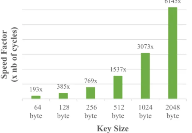
key sizes: 64, 128, 256, 512 and 1024 byte. In Figure 7, we present the timing speed factor of the IMPACT system com-pared to the conventional one. The acceleration of IMPACT emulation varies between 193x and 6145x times. On the other hand, the gain in the energy consumption is about 12.9x times the energy consumed by conventional system. The energy reduction does not vary when the workload data size change, since it is measured by words of data.
193x 385x 769x 1537x 3073x 6145x 64
byte 128byte 256byte 512byte 1024byte 2048byte
Sp ee d F ac tor (x nb of c yc les) Key Size
Figure 7: Timing speed factor between conventional and IMPACT systems for OTP application
5.2
Motion Detection
Motion detection [11] has attracted a great interest from computer vision researchers due to its promising applications in many areas, such as video surveillance, traffic monitoring or sign language recognition. Motion detection represents the basis of any object tracking, or image compression system. It is defined as the process of detecting a change in the object position relative to its surroundings or a change in the surroundings relative to an object.
The motion detection algorithm used in this paper consists in comparing the pixels of the image sequence frame in order to detect (or not) a movement in a certain zone of the image. As shown in Algorithm 2, the comparison of the images is performed by subtraction operation. The pixel colors of the resulting image represent the degree of difference between the two images.
The algorithm is implemented as conventional and IM-PACT implementations. For the conventional version, the image is implemented as a matrix of pixels, each pixel is of 1 byte. The subtraction is then performed byte per byte on the matrix pixels. The complexity of the memory access is quadratic (O(N2
)). However, for the IMPACT version, the image is implemented as an array of vectors. The vectors represent the lines of the image pixels. The subtraction is then performed vector per vector. The complexity of the memory access is then linear (O(N)).
For the experiments, we consider images with different sizes:
Algorithm 2 Motion Detection (Conventional Version)
1: unsigned char Img[LARGEUR*4][HAUTEUR]
2: for (line = 0; line<HAUTEUR; ++line) do
3: for (column = 0; column<LARGEUR; ++column) do
4: for (i=0; i<4; i++) do
5: Img[line][column*4+i] = ImgA[line][column*4+i] - ImgB[line][column*4+i]
6: end for
7: end for
8: end for
• X264 Standard of video compression: block sizes of 16x16 and 8x8 pixels.
• Graphics Display Resolution: 160x120 QQVGA, 320x240 QVGA, 640x480 VGA.
• High Definition: 960x540 qHD.
In Figure 8, we present the clock cycle speed factor of the IMPACT system compared to the conventional one. The results show that the acceleration varies between 50x and 5952x times the timing of the conventional system. The gain in the energy consumption is about 12.4x times the energy consumed by the conventional system. The energy reduction does not vary when the workload data size change, since it is measured by words by data.
50x 100x 992x 1984x 3968x 5952x 8x8
X264 16x16X264 160x120QQVGA320x240QVGA 640x480VGA 960x540qHD
Sp ee d F ac tor (x nb of c yc les) Image Size
Figure 8: Timing speed factor between conventional and IMPACT systems for motion detection applica-tion
5.3
Discussion
We note from the presented results that the timing accel-eration is more important for larger application workloads. Since we assume in this paper that the IMPACT memory is designed as single block, we have to design very large size IMPACT memories to run big data applications, which leads to increase the timing acceleration of the IMPACT memory. However, this is quite costly in particular for IMPACT circuit that are designed to be more complex than conventional cir-cuits since it contains additional circir-cuits that are responsible to perform operations. A possible solution that we envisage
as a perspective to this work is to partition and design several IMPACT memory blocks with reasonable word size, then distribute the data workload on these blocks in a way to maximize the parallel operations. For example, the memory blocks can be superposed in 3D. An operation in one block can be then performed in parallel as an other operation in a second block. In particular, we can simulate the motion detection application on images of type VGA, using four images of type quarter VGA (QVGA) distributed on four memory blocks. The timing acceleration will be significant thanks to the parallelization, while the cost of the memory design will be reduced.
We note also from these results that the IMPACT system offers significant timing accelerations while less significant gain in the energy consumption. In fact, the energy study presented in this paper is preliminary. We need to investigate more effort to have more precise and significant gains in energy consumption, while keeping important timing acceler-ations.
As mentioned previously in Section 4, the acceleration factors shown in Figure 7 and 8 represent the execution time of the function that is performing the arithmetic/logic data computation. It will be interesting, in future work, to consider the rest of the application and also the rest of the system. The speed factor will be reduced relatively while remaining significant compared to a conventional system.
6
CONCLUSION
In this paper, we presented a new software platform able to dimension and evaluate our IMPACT circuit. The proposed approach permits to manually convert a software application from conventional implementation to IMPACT implementa-tion, using an equivalent vector-parallel representation. The two implementations are then compiled to the middleware LLVM IR and instrumented in order to record traces of each execution. The traces are then analyzed to evaluate the per-formance of IMPACT circuit in terms of timing and energy consumption. In this paper, we present two application sce-narios to experiment the IMPACT circuit: (1) a security application presenting input data of one dimension, and (2) an image processing application presenting input data of two dimensions.
The results of emulating these applications on IMPACT circuit show a significant gain in the execution time and a quite important gain in the energy consumption comparing to a conventional system run on an ARM Cortex®-M7 pro-cessor. The timing acceleration varies between 50x and 6145x, while the energy speed factor is about 12.6x.
As perspective, several ideas can be developed. First, we propose to investigate effort to have more important and precise energy gain. Furthermore, we propose to partition the IMPACT memory in different blocks with small word size in order to parallelize the execution of operations, which should improve the system performance.
REFERENCES
[1] [n. d.]. ARM: Architecture for the Digital World, Cortex-M7 Processor. www.arm.com/products/processors/cortex-m/ cortex-m7-processor.php. ([n. d.]).
[2] [n. d.]. clang: a C language family frontend for LLVM. www.clang. llvm.org/. ([n. d.]).
[3] [n. d.]. LLVM Language Reference Manual. www.llvm.org/docs/ LangRef.htmlinteger-type. ([n. d.]).
[4] Shaizeen Aga et al. 2017. Compute Caches. In IEEE Interna-tional Symposium on High Performance Computer Architecture (HPCA). 481–492.
[5] Kaya Can Akyel et al. 2016. DRC 2: Dynamically Reconfigurable Computing Circuit based on memory architecture. In IEEE In-ternational Conference on Rebooting Computing (ICRC). 1–8. [6] Maya Gokhale et al. 1995. Processing in memory: The Terasys
massively parallel PIM array. Computer 28, 4 (1995), 23–31. [7] Joe Jeddeloh and Brent Keeth. 2012. Hybrid memory cube new
DRAM architecture increases density and performance. In Sym-posium on VLSI Technology (VLSIT). 87–88.
[8] Supreet Jeloka et al. 2016. A 28 nm Configurable Memory (TCAM/BCAM/SRAM) Using Push-Rule 6T Bit Cell Enabling Logic-in-Memory. IEEE Journal of Solid-State Circuits 51, 4 (2016), 1009–1021.
[9] Dongsuk Jeon et al. 2017. A 23-mW Face Recognition Processor with Mostly-Read 5T Memory in 40-nm CMOS. IEEE Journal of Solid-State Circuits 52, 6 (2017), 1628–1642.
[10] V Joshi et al. 2017. Low-variation SRAM bitcells in 22nm FDSOI technology. In Symposium on VLSI Technology. IEEE, T222– T223.
[11] Kamna Kohli and Jatinder Pal Singh. 2013. Motion Detection Algorithm. International Journal of Computer Science & Ap-plications (TIJCSA) 1, 12 (2013).
[12] Maha Kooli. 2016. Analysing and Supporting the Reliability Decision-making Process in Computing Systems with a Relia-bility Evaluation Framework. Theses. Universit´e Montpellier. [13] Chris Lattner and Vikram Adve. 2004. LLVM: A compilation
framework for lifelong program analysis & transformation. In Proceedings of the international symposium on Code generation and optimization: feedback-directed and runtime optimization. IEEE Computer Society, 75.
[14] Dominique Lavenier et al. 2016. DNA Mapping using Processor-in-Memory Architecture. In Workshop on Accelerator-Enabled Al-gorithms and Applications in Bioinformatics. Shenzhen, China. [15] Shuangchen Li et al. 2016. Pinatubo: A processing-in-memory
architecture for bulk bitwise operations in emerging non-volatile memories. In 53nd ACM/EDAC/IEEE Design Automation Con-ference (DAC). 1–6.
[16] Shoun Matsunaga et al. 2009. MTJ-based nonvolatile logic-in-memory circuit, future prospects and issues. In Proceedings of the Conference on Design, Automation and Test in Europe. European Design and Automation Association, 433–435. [17] David Patterson et al. 1997. A case for intelligent RA. IEEE
Micro 17, 2 (1997), 34–44.
[18] Seth H Pugsley et al. 2014. NDC: Analyzing the impact of 3D-stacked memory + logic devices on MapReduce workloads. In IEEE International Symposium on Performance Analysis of Systems and Software (ISPASS). 190–200.
[19] Bruce Schneier. 2007. Applied cryptography: protocols, algo-rithms, and source code in C. john wiley & sons.
[20] Yuhao Wang et al. 2016. DW-AES: A Domain-Wall Nanowire-Based AES for High Throughput and Energy-Efficient Data En-cryption in Non-Volatile Memory. IEEE Transactions on Infor-mation Forensics and Security 11, 11 (2016), 2426–2440. [21] Qiuling Zhu et al. 2013. A 3D-stacked logic-in-memory
acceler-ator for application-specific data intensive computing. In IEEE International 3D Systems Integration Conference (3DIC). 1–7.