HAL Id: hal-00796266
https://hal.archives-ouvertes.fr/hal-00796266
Submitted on 2 Mar 2013
HAL is a multi-disciplinary open access
archive for the deposit and dissemination of
sci-entific research documents, whether they are
pub-lished or not. The documents may come from
teaching and research institutions in France or
abroad, or from public or private research centers.
L’archive ouverte pluridisciplinaire HAL, est
destinée au dépôt et à la diffusion de documents
scientifiques de niveau recherche, publiés ou non,
émanant des établissements d’enseignement et de
recherche français ou étrangers, des laboratoires
publics ou privés.
Silicon nanowires as negative electrode for lithium-ion
microbatteries
Barbara Laik, Laurent Eude, Jean Pierre Pereira-Ramos, Costel Sorin
Cojocaru, Didier Pribat, Emmanuelle Rouvière
To cite this version:
Barbara Laik, Laurent Eude, Jean Pierre Pereira-Ramos, Costel Sorin Cojocaru, Didier Pribat, et al..
Silicon nanowires as negative electrode for lithium-ion microbatteries. Electrochimica Acta, Elsevier,
2008, 53 (17), pp.5528–5532. �10.1016/j.electacta.2008.02.114�. �hal-00796266�
Electrochimica Acta
53 (2008) 5528–5532
DOI:
http://dx.doi.org/10.1016/j.electacta.2008.02.114
Silicon nanowires as negative electrode for lithium-ion
microbatteries
Barbara La¨ık
a,∗, Laurent Eude
b, Jean-Pierre Pereira-Ramos
a, Costel Sorin Cojocaru
b, Didier Pribat
b, Emmanuelle Rouvie` re
c
a Institut de Chimie et des Mate´riaux Paris Est, ICMPE/GESMAT, UMR 7182 CNRS-Universite´ Paris XII, 2 rue Henri Dunant, 94320 Thiais, France b Laboratoire de Physique des Interfaces et Couches Minces, LPICM, UMR 7647 E´cole Polytechnique-CNRS, Route de Saclay, 91128 Palaiseau Cedex, France c Laboratoire des Composants Hybrides, LCH, CEA-DRT/LITEN/DTNM, 17 rue des martyrs, 38054 Grenoble Cedex, France
A B S T R A C T
KEYWORDS:
Lithium batteries,
Silicon,
Si nanowires,
Thin films
The increasingly demand on secondary batteries with higher specific energy densities requires the replace- ment of the actual electrode materials. With a very high theoretical capacity (4200 mAh g1 ) at low voltage, silicon is presented as a very interesting potential candidate as negative electrode for lithium-ion micro- batteries. For the first time, the electrochemical lithium alloying/de-alloying process is proven to occur, respectively, at 0.15 V/0.45 V vs. Li+ /Li with Si nanowires (SiNWs, 200–300 nm in diameter) synthesized by
chemical vapour deposition. This new three-dimensional architecture material is well suited to accom- modate the expected large volume expansion due to the reversible formation of Li–Si alloys. At present, stable capacity over ten to twenty cycles is demonstrated. The storage capacity is shown to increase with the growth temperature by a factor 3 as the temperature varies from 525 to 575 ◦ C. These results, showing an attractive working potential and large storage capacities, open up a new promising field of research.
1. Introduction
The current commercial lithium-ion secondary batteries are the most widely used because of their higher energy density, their higher operating voltages and their lower self-discharge [1,2]. They are based on an anode made of graphitic carbon or other carbona- ceous materials that present on the one hand the advantage to be cheap and on the other hand interesting electrochemical properties such as a low and flat working voltage and a good cycleability. How- ever, the maximal insertion of one lithium ion for six carbon atoms leads to a theoretical capacity limited to 372 mAh g1 , which is rel- atively low. In order to satisfy to the increasingly demand for new compact and modern portable electronic devices, both the active materials in the cathode and the anode should be replaced by new materials.
Concerning the anodic materials, metals, metalloids and semi- conductors such as Sn, Al, Sb and Si which can make alloys with lithium, are attractive alternatives to graphite due to their low cost and high storage energy density. Theoretical specific capaci- ties more than ten times higher than with carbon can be obtained. However, the structural changes and a large volume expansion associated with lithium insertion, which can rise to more than 300% (whereas it is below 10% for LiC6 ) [3], limit the ability of
.
these materials to cycle with high efficiency. Indeed, successive charge–discharge cycles lead to mechanical stresses in the elec- trode and finally to the destruction of its structural integrity and to the consequent loss of electronic particle to particle contact [4–6].
Among the above materials, silicon has the highest specific capacity since it is capable to form compounds which can insert up to 4.2 lithium per silicon. Its theoretical capacity is as high as 4200 mAh g1 [7–9]. Moreover, the electrochemical curves obtained during the insertion/deinsertion of lithium into/from sil- icon are roughly flat as it is with graphite and in a low voltage range 0.4/0.02 V, that makes Si very attractive [10–12]. Li alloying in crystalline Si is known to induce the formation of new inter- metallic phases leading to inhomogeneous volume expansions in the two-phase regions and then to cracking and pulverization of the material [13,14]. As a consequence of this cracking, there is a loss of inter-particles electrical contact inducing a significant capacity decline. Therefore, the loss of electric contact is still a crucial hurdle that must be overcome in order to improve the cycleability during further alloying/de-alloying reactions.
Different ways have been tested to solve the problem of cycle life by coating the surface of Si with various conducting mate- rials [15–17], by modifying the substrate surface properties with adapted treatments to improve the adhesion of the Si film [18,19] or by using for instance composite electrodes in which secondary components (carbon, copper, tin, etc.) are added to obtain mechan- ical stability, to enhance the electronic conduction or to improve the ionic or atomic transport [14,20–23].
Another trend for improving the cycle life of Si consists in using amorphous Si. Indeed in amorphous alloys the volume expansion on Li insertion is reported to be homogeneous with- out pulverization like in the crystalline material [13,14]. This view is not supported by all the authors [24] but recent studies have demonstrated that the amorphous Si thin film electrodes showed improved electrochemical performance [12,19,25–30]. As far as applications are concerned, these films are too thin (<500 nm) to provide sufficient capacity and the way to expand the film thickness without sacrificing cycleability and specific capacity constitutes an important issue. Only a few recent encouraging data are available for thick films. The best results are found for films, in the range 1–5 J.Lm thick, deposited on Cu by vacuum deposition [19] or chem- ical vapour deposition [29,30], and by electron-beam deposition [31]. Capacities available with those thicker films and included in the realm 1200–1500 mAh g1 can be stabilized over 100–200 cycles while stability for larger capacities does not exceed ten to a few tenths of cycles [32]. In fact, to date, no research group has definitively established that the theoretical capacity can be stabi- lized over a large number of cycles.
A new approach consists in using a three-dimensional archi- tecture which allows combining the accommodation of the large volume changes expected for Li insertion in crystalline silicon with a continuous and efficient electrical contact between Si particles. Porous silicon electrodes have been considered and tested in this way [33,34]. In the same frame of mind, Si nanowires as an emerg- ing structure, offers advantages of large surface to ratio volume, efficient electron conducting pathways, shorter diffusion pathways for lithium and facile strain relaxation, what let us believe that silicon nanowires (SiNWs) could be a potential candidate to opti- mize the electrochemical performance of the Si negative electrode and to replace carbonaceous materials. Si nanowires (SiNWs) are a new class of materials currently studied within the context of molecular electronics. Typically, the diameter of such nanowires range between a few nm and few hundreds of nanometers. As they exhibit excellent electrical characteristics, nanowire-based transis- tors could replace classical CMOS devices in the near future [35].
To date and to the best of our knowledge, no paper deals with electrochemical characteristics of SiNWs as anodic material for a Li-ion battery. Actually, only the structural changes of this nanos- tructured material have already been investigated (for doping and contacting purposes) by high-resolution electron microscopy at different lithium alloying/de-alloying levels controlled by an elec- trochemical method [36].
In this work we demonstrate for the first time the feasibility of using Si nanowires as negative electrode for Li-ion batteries, which opens up a new field of research for the development of the micro- batteries.
2. Experimental
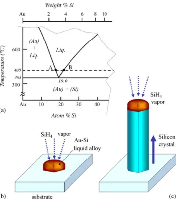
SiNWs are synthesized by chemical vapour deposition (CVD) according to the vapour–liquid–solid (VLS) growth mechanism which has been extensively studied ~40 years ago by Wagner [37] for the growth of whiskers. This mechanism can be explained with
Fig. 1. Schematic mechanism of the VLS growth process: (a) the Au–Si phase dia-
gram on the Au-rich side. (b and c) Formation of the liquid drop and growth of the Si whisker (see text for more details).
rapidly reached, where the flux of Si atoms incorporated at the surface of the liquid alloy is balanced by the flux of Si atoms precip- itating at the liquid–solid interface. As the liquid surface behaves as an ideally rough surface, the sticking coefficient of the gaseous SiH4 molecules is close to 1, resulting in a highly anisotropic growth
that explains the whisker shape obtained (Fig. 1c). The Au–Si liq- uid drop rises on top of the crystal and appears spherical in shape due to surface tension effects. The feasibility of Si nanowire growth by the VLS mechanism has been demonstrated recently using gold clusters [38].
The substrates used in this study were commercial stainless steel (316 L) foils of 50 J.Lm thickness. Prior to CVD growth of SiNWs, 50 nm of Ti as an adhesive layer and 100 nm of TiN as a conduc- tive diffusion barrier were deposited on the substrates, followed by a 10 nm-thick Au film, using a magnetron sputtering system. The substrates were then loaded in a CVD furnace and heated under vac- uum (base pressure less than 105 mbar) above the Au–Si eutectic melting temperature (in this study, we used three different temper- atures, namely 525, 550 and 575 ◦C). During this treatment, the Au thin film transforms into clusters of various sizes, in order to reduce the superficial/interfacial energy with TiN. Then, SiH4 diluted at 5%
in hydrogen (H2 ) is injected in the furnace for 15 min at a total flow
of 100 sccm and total pressure of 15 mbar.
Electrochemical studies were carried out in a two-electrode
®
the help of Fig. 1. A Si bearing gas (e.g. SiH4 ) is allowed to flow over cell (Swagelok type). This cell was prepared inside a dry box by
catalyst clusters (e.g. Au) deposited on a chemically inert substrate which is heated above the catalyst-Si eutectic melting tempera- ture. Some SiH4 molecules decompose by pyrolysis and some of
the released Si atoms adsorb on the catalyst dots and alloy with the surface atoms. As more Si is brought to the catalyst surface, the alloy composition evolves towards the eutectic composition. Melting starts to occur (Fig. 1a), rapidly consuming the whole cat- alyst dot. Continued feed of Si makes the alloy composition evolve towards saturation, inducing Si precipitation. An equilibrium is
placing a clean lithium metal disk (7 mm diam.), a glass fiber sep- arator soaked with the electrolyte solution, and the cathode film (0.28 cm2 ) into a Teflon container with two stainless steel termi-
nals. The electrolyte used was 1 mol L1 LiClO4 , dried under vacuum
at 180 ◦C for 15 h, dissolved in twice-distilled propylene carbon- ate obtained from Fluka. Galvanostatic measurements were made with a computer controlled 1470 A Solartron potentiostat. A con- stant current density of 35 J.LA cm2 was used for charge–discharge experiments.
3. Results and discussion
Fig. 2. SEM observations of SiNWs films obtained at 550 ◦ C.
A SEM image of the thin SiNWs grown at 550 ◦C is displayed in Fig. 2. It can be seen that SiNWs with diameters up to 300 nm are uniformly obtained on the surface of the TiN-covered substrate. The small Au droplets used as catalyst for the growth of Si wires and whose size mainly controls their diameter are still present and they can be observed at the top of the nanowires.
The Raman spectrum of the as-deposited SiNWs is shown in Fig. 3. A well defined and symmetric peak at 520.1 cm1 corre- sponding to the first order Raman line for crystalline silicon is observed which ascertains very well crystallized SiNWs are pre- pared [39].
Before testing the SiNWs as active electrode material against Li alloying, we have evaluated the possible electrochemical con- tribution of the Au droplets still present at the top of the silicon wires after synthesis. Indeed even when only a little is known on the electrochemical properties of Li–Au alloys at room tempera- ture, the Au electrode has been recently proved to accommodate Li in the 0.02–0.5 V potential range with a poor reversibility [40,41]. The discharge–charge curves obtained for a 50 nm thick gold film are shown in Fig. 4. Two voltage plateaus corresponding to the Li alloying process into two different phases are observed at 0.2 and 0.1 V while Li removal from the alloy takes place in two steps at 0.18 and 0.4 V in good agreement with Refs. [40,41]. The poor effi- ciency of the charge process is clearly evidenced since only 50% of the faradaic yield involved in the alloying reaction is recovered at
Fig. 3. Raman spectrum of SiNWs films obtained at 550 ◦ C.
Fig. 4. Typical voltage curve of a 50 nm thick gold film discharged/charged between
0.02 and 1 V and the capacity vs. cycle number for a 10 nm thick gold film in the inset.
1 V. For a 10 nm thick gold film, as used here for the SiNWs growth, the evolution of the capacity obtained during the cycling exper- iments as a function of cycle number is reported in the inset of Fig. 4. At 35 J.LA cm2 , the coulombic charge drastically decreases from 170 mC to reach a few tenths of mC after less than 15 cycles.
The electrochemical properties of SiNWs have been studied for different temperature of deposition. The typical discharge–charge curves presented in Fig. 5 (cycles 1, 2, 5 and 10) are related to a sam- ple deposited at 525 ◦C. A part of the coulombic charge involved for potentials upper than 0.5 V during the first reduction is usu- ally ascribed to the formation of a solid electrolyte interphase (SEI) stemming from the decomposition products of the liquid electrolyte. This irreversible phenomenon depends on the silicon surface which can be covered with a native layer consisting of silicon oxide (–Si–O–Si–) and silanol (–Si–OH) [42] and the cor- responding capacity equals in this case about 150 mC. At lower potentials, the initial lithiation of crystalline silicon results in a sin- gle low voltage plateau located at 0.15 V. From literature data on the electrochemical reaction of lithium with silicon, according to the equilibrium Li–Si phase diagram, four distinct open circuit voltage (OCV) curves corresponding to the successive formation of Li12 Si7 ,
Li7 Si3 , Li13 Si4 , Li21 Si5 could be expected [9,43]. Due to the very close
Fig. 5. Voltage curves of a SiNWs film obtained at 525 ◦ C discharged/charged between 0.02 and 3 V (cycles 1, 2, 5, 10) and the corresponding capacity vs. cycle number in the inset.
constant current. According to recent galvanostatic studies [44,45], the 0.15 V voltage plateau observed in Fig. 5 could correspond to the lithiation of crystalline Si leading to an amorphous a-Lix Si phase. At
the end of the discharge, i.e. for Q > 700 mC (Fig. 5), the crystalline Li13 Si4 phase could be formed as suggested by a very recent study
performed on crystalline silicon powder [46].
The delithiation reaction mainly results in a voltage plateau at 0.45 V corresponding to the formation of silicon. From the second cycle, two reduction steps are observed at 0.25 and 0.1 V, whereas the oxidation keeps the same profile as during the first cycle. As a conclusion, these preliminary electrochemical data are in a good agreement with those known for the reversible Li alloying/de- alloying reaction in crystalline silicon [44–46]. In other respects, it can be pointed out that the two small reduction and oxidation steps at, respectively, 0.2 and 0.16 V probably reveal the contribu- tion of the Li–Au system resulting from the Au droplets at the top of the nanowires. Nevertheless, our previous experiments performed on Au films show that this contribution cannot exceed 40 mC at the best, i.e. ~10% of the capacity (inset in Fig. 4).
Without taking into account the loss of capacity ascribed to the SEI formation, the inset in Fig. 5 demonstrates that a satisfactory
Fig. 6. Voltage curves of a SiNWs film obtained at 550 ◦ C discharged/charged between 0.02 and 3 V (cycles 1, 2, 5, 10) and the corresponding capacity vs. cycle number in the inset.
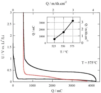
Fig. 7. Voltage curves of a SiNWs film obtained at 575 ◦ C discharged/charged between 0.02 and 3 V (cycle 1 in dark line, second reduction in dashed line) and the capacity vs. SiNWs deposition temperature in the inset.
capacity retention can be achieved with SiNWs since 400 mC are still available after 20 cycles.
The electrochemical behaviour of the sample synthesized at 550 ◦C is quite the same as the sample described above except the significantly higher capacity (1750 mC) achieved in the same volt- age range (Fig. 6). This could be related to an increase of the SiNWs growth rate at higher temperature leading to a greater amount of deposited Si. A slow decline of the faradaic yield with cycles is observed but more than 750 mC are still available after 20 cycles.
The capacity value can still be increased as shown by the elec- trochemical behaviour of a sample with SiNWs grown at 575 ◦C (Fig. 7). Indeed, without taking into account irreversible capacity in the first cycle (same order of magnitude whatever the tem- perature of growth of SiNWs), a capacity as high as 3200 mC, i.e. around 3000 J.LAh cm2 is reached with a satisfactory efficiency of the charge process. Such an attractive electrochemical behaviour makes it possible to use SiNWs in secondary Li microbatteries based on thin film metal oxides as positive electrodes and characterized, for thick films, by capacities of about 250–300 J.LAh cm2 at best. The quasi-linear relationship between capacity and SiNWs syn- thesis temperature indicates a possible control of the effective Si surface deposit during the growth process and suggests that an
Fig. 8. SEM images (same magnification) of unlithiated SiNWs (inset) and fully
optimization of the capacity is possible. The influence of several parameters like the length and the diameter of the SiNWs, the den- sity of the deposit and their crystallinity must be considered in details, making possible a future application of SiNWs as negative electrode for rechargeable Li-ion batteries.
Moreover, a study of the modifications of the SiNWs structural morphology during both lithiation and delithiation is required in order to reveal possible damages in the 3D architecture conse- quently to the successive insertion/deinsertion of lithium which could be responsible of the decrease of the capacity. The SEM micrography of fully lithiated SiNWs obtained by stopping the elec- trochemical cycle after a full discharge, i.e. at 0.02 V, is presented in Fig. 8 and compared to the micrography of the starting material (inset). As expected, statically, wires seem to be larger in diameter when they are lithiated. A further complete study in under progress to determine the size distribution of the SiNWs and the average diameter, for different amounts of lithium inserted in the wires during both the discharge and the charge, for successive cycles.
4. Conclusion
In this paper, we have reported the first electrochemical results on the use of SiNWs as negative electrode for rechargeable lithium microbatteries. Until now and to the best of our knowledge, such results have never been reported in the literature. We have shown that SiNWs constitute a new possibility for building a three- dimensional negative electrode of great interest for rechargeable Li microbatteries. The SiNWs electrochemical behaviour resem- bles that known for crystalline silicon. It presents an attractive working potential (<0.5 V vs. Li+ /Li) and large storage capacities (a few thousands of mC). Though the reversible Li alloying/de- alloying is ensured right now on more than ten cycles with good charge–discharge efficiency, a significant decrease of the capac- ity takes place with further cycling. We have also shown that the available storage capacity strongly depends on the SiNWs growth temperature and increases with it. These preliminary and promis- ing results call for a further insight into the Li alloying/de-alloying mechanism in order to investigate and to understand both the elec- trochemical and structural response of SiNWs vs. Li content, the discharge–charge rate, cycling.
Acknowledgment
This work was partially supported by the French ANR contract “NANOBAT2”.
References
[1] G.-A. Nazri, G. Pistoia, in: G. Pistoia (Ed.), Lithium batteries : Science and Tech- nology, Kluwer Academic Publishers, 2004, p. 113.
[2] J.M. Tarascon, M. Armand, Nature 414 (2001) 359. [3] J.L. Tirado, Mater. Sci. Eng. R 40 (2003) 103.
[4] M. Winter, J.O. Besenhard, Electrochim. Acta 45 (1999) 31. [5] J.O. Besenhard, J. Yang, M. Winter, J. Power Sources 68 (1997) 87.
[6] L.Y. Beaulieu, K.W. Eberman, R.L. Turner, L.J. Krause, J.R. Dahn, Electrochem. Solid State Lett. 4 (2001) A137.
[7] W.G. Moffat, The Handbook of Binary Phase Diagrams, Genium Publishing Corp., Schenectady, New York, 1990.
[8] J.O. Besenhard, in: T. Besenhard (Ed.), Handbook of Battery Materials, Wiley- VCH, Weiheim, 1999, p. 363.
[9] W.J. Weydanz, M. Wohlfahrt-Mehrens, R.A. Huggins, J. Power Sources 81–82 (1999) 237.
[10] M. Winter, J.O. Besenhard, M.E. Spahr, P. Novak, Adv. Mater. 10 (1998) 725. [11] Y. Kubota, M.C.S. Escano, H. Nakanishi, H. Kasai, J. Alloy Compd. 434–435 (2007)
294.
[12] S. Ohara, J. Suzuki, K. Sekine, T. Takamura, J. Power Sources 119–121 (2003) 591. [13] T.D. Hatchard, J.R. Dahn, J. Electrochem. Soc. 151 (2004) A838.
[14] L.Y. Beaulieu, T.D. Hatchard, A. Bonakdarpour, M.D. Fleischauer, J.R. Dahn, J. Electrochem. Soc. 150 (2003) A1457.
[15] J.W. Kim, J.H. Ryu, K.T. Lee, S.M. Oh, J. Power Sources 147 (2005) 227. [16] M. Yoshio, H. Wang, K. Fukuda, T. Umeno, N. Dimov, Z. Ogumi, J. Electrochem.
Soc. 149 (2002) A1598.
[17] W.-R. Liu, J.-H. Wang, H.-C. Wu, D.-T. Shieh, M.-H. Yang, N.-L. Wu, J. Electrochem. Soc. 152 (2005) A1719.
[18] H.X. Deng, C.Y. Chung, Y.T. Xie, P.K. Chu, K.W. Wong, Y. Zhang, Z.K. Tang, Surf. Coat. Technol. 201 (2007) 6785.
[19] T. Takamura, M. Uehara, J. Suzuki, K. Sekine, K. Tamura, Power Sources J. 158 (2006) 1401.
[20] Y. Liu, K. Hanai, J. Yang, N. Imanishi, A. Hirano, Y. Takeda, Electrochem. Solid State Lett. 7 (2004) A369.
[21] M. Yoshio, T. Tsumura, N. Dimov, J. Power Sources 146 (2005) 10. [22] M.K. Datta, P.N. Kumta, J. Power Sources 158 (2006) 557.
[23] L.Y. Beaulieu, K.C. Hewitt, R.L. Turner, A. Bonakdarpour, A.A. Abdo, L. Chris- tensen, K.W. Eberman, L.J. Krause, J.R. Dahn, J. Electrochem. Soc. 150 (2003) A149.
[24] S. Bourderau, T. Brousse, D.M. Schleich, J. Power Sources 81–82 (1999) 233. [25] T. Takamura, S. Ohara, M. Uehara, J. Suzuki, K. Sekine, J. Power Sources 129
(2004) 96.
[26] V. Baranchugov, E. Markevich, E. Pollak, G. Salitra, D. Aurbach, Electrochem. Commun. 9 (2007) 796.
[27] T.L. Kulova, A.M. Skundin, Y.V. Pleskov, E.I. Terukov, O.I. Kon’kov, J. Electroanal. Chem. 600 (2007) 217.
[28] H. Guo, H. Zhao, C. Yin, W. Qiu, Mater. Sci. Eng. 131 (2006) 173.
[29] T. Yoshida, T. Fujihara, H. Fujimoto, R. Ohshita, M. Kamino, S. Fujitani, Abstract No 48, Proceedings of the 11th IMLB, Monterey, CA, June 23–28, 2002. [30] I. Yonezu, H. Tarui, S. Yoshimura, S. Fujitani, T. Nohma, Abstract No 58, Proceed-
ings of the 12th IMLB, Nara, Japan, June 27–July 2, 2004.
[31] J. Yin, M.W. Koichi Yamamoto, Y. Kitano, S. Tanase, T. Sakai, J. Electrochem. Soc. 153 (2006) A472.
[32] J.P. Maranchi, A.F. Hepp, P.N. Kumta, Electrochem. Solid State Lett. 6 (2003) A198.
[33] H.-C. Shin, J.A. Corno, J.L. Gole, M. Liu, J. Power Sources 139 (2005) 314. [34] M. Green, E. Fielder, B. Scrosati, M. Wachtler, J.S. Moreno, Electrochem. Solid
State Lett. 6 (2003) A75.
[35] Y. Cui, Z. Zhong, D. Wang, W.U. Wang, C.M. Lieber, Nano Lett. 3 (2003) 149.
[36] G.W. Zhou, H. Li, H.P. Sun, D.P. Yu, Y.Q. Wang, X.J. Huang, L.Q. Chen, Z. Zhang, Appl. Phys. Lett. 75 (1999) 2447.
[37] R.S. Wagner, in: A.L. Svitt (Ed.), Whisker Technology, Wiley Intersciences, New York, 1970, p. 47.
[38] Y. Cui, L.J. Lauhon, M.S. Gudiksen, J. Wang, C.M. Lieber, Appl. Phys. Lett. 78 (2001) 2214.
[39] J. Niu, J. Sha, Z. Liu, Z. Su, J. Yu, D. Yang, Physica E 24 (2004) 268.
[40] G. Taillades, N. Benjelloun, J. Sarradin, M. Ribes, Solid State Ionics 152–153 (2002) 119.
[41] L. Yuan, H.K. Liu, A. Maaroof, K. Konstantinov, J. Liu, M. Cortie, J. New Mater. Electrochem. Syst. 10 (2007) 95.
[42] Y.M. Lee, J.Y. Lee, H.-T. Shim, J.K. Lee, J.-K. Park, J. Electrochem. Soc. 154 (2007) A515.
[43] C.J. Wen, R.A. Huggins, J. Solid State Chem. 37 (1981) 271. [44] M.N. Obrovac, L.J. Krause, J. Electrochem. Soc. 154 (2007) A103. [45] M.N. Obrovac, L. Christensen, Electrochem. Solid State Lett. 7 (2004) A93. [46] J. Li, J.R. Dahn, J. Electrochem. Soc. 154 (2007) A156.