HAL Id: hal-01933337
https://hal.archives-ouvertes.fr/hal-01933337
Submitted on 23 Nov 2018HAL is a multi-disciplinary open access
archive for the deposit and dissemination of sci-entific research documents, whether they are pub-lished or not. The documents may come from teaching and research institutions in France or abroad, or from public or private research centers.
L’archive ouverte pluridisciplinaire HAL, est destinée au dépôt et à la diffusion de documents scientifiques de niveau recherche, publiés ou non, émanant des établissements d’enseignement et de recherche français ou étrangers, des laboratoires publics ou privés.
Combined EPR and photoluminescence study of
electron and proton irradiated 3C-SiC
Abdul Salam Al Atem, Victor Bratus, Bruno Canut, Jérémie Lefèvre, G
Guillot, Jean-Marie Bluet
To cite this version:
Abdul Salam Al Atem, Victor Bratus, Bruno Canut, Jérémie Lefèvre, G Guillot, et al.. Combined EPR and photoluminescence study of electron and proton irradiated 3C-SiC. 12 th European Conference on Silicon Carbide and Related Materials(ECSCRM), 2018, Birmingham, United Kingdom. �hal-01933337�
ID: 1285
(ID number can be found on the submission page.)
Combined EPR and photoluminescence study of electron and proton
irradiated 3C-SiC
A. AL ATEM
1), V. Bratus
2)B. Canut
1), J. Lefevre
3), G. Guillot
1), and J-M Bluet
1) 1) Université de Lyon, Institut des Nanotechnologies de Lyon, CNRS UMR5270,
INSA de Lyon, Bat. Blaise Pascal, 7 avenue Capelle, F-69621 Villeurbanne Cedex,
France.
2
) Department of Optics and Spectroscopy, V. Lashkaryov Institute of Semiconductor
Physics,National Academy of Sciences of Ukraine, 45 pr. Nauky, 03680 Kyiv,
3)
Ecole Polytechnique de Paris, Laboratoire des Solides Irradiés, CEA-IRAMIS,
CNRS, F-91128 Palaiseau Cedex, France.
E-mail:
1)abdul-salam.al-atem@insa-lyon.fr,
2)v_bratus@isp.kiev.ua,
1)bruno.canut@insa-lyon.fr,
3)jeremie.lefevre@polytechnique.edu,
1)gerard.guillot@insa-lyon.fr,
1)jean-marie.bluet@insa-lyon.fr
In past few years, point defects in silicon carbide (SiC) have been identified as promising for applications in quantum technologies [1]. A variety of point defects in hexagonal SiC [2], including VSi and VSiVC have been optically isolated and used as single defect-based spin qubits with long
coherence time [3-5]. All of this, proves that these point defects allow the SiC to be a very favorable candidate for quantum applications especially, solid state quantum bits (Qubits) and single photon source (SPS). Most of these studies were carried out on the hexagonal polytypes 4H-SiC and 6H-SiC, although the 3C-SiC polytype presents the unique advantage of integration possibility on standard Si wafer. This is due to the amount of defects (dislocation mainly) in the 3C-SiC heteroepitaxy on Si which are detrimental for long coherence time considering Qubit application.
Consequently, the goal of the present study is the investigation of point defects formation after implantation by proton H+ (300 keV) and irradiation by electron e- (0.8 and 2 MeV) in 3C-SiC
(respectively 3C-SiC<p> and 3C-SiC<e>) for SPS application purpose. Toward this end, we have combined two characterization techniques, the photoluminescence (PL) and the electron paramagnetic resonance (EPR). PL (12K) and EPR (70-300K) measurements will be presented in order to analyze precisely the signatures of point defects generated after these two types of irradiations. The effects of the thermal annealing (500 -1000°C) were also investigated.
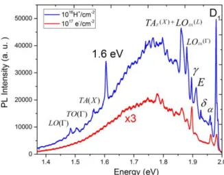
PL spectra both for 3C-SiC<p> and 3C-SiC<e> are presented in figure 1 for the annealing temperatures giving the highest PL signal (1000°C for 3C-SiC<p> and 750°C for 3C-SiC<e>). We notice first that the whole PL signal is higher for 3C-SiC<p>. In this case the spectrum is dominated by the DI defect line (possibly related to antisite pair [6]) and the E line (attributed to Si vacancy [7,
8]) while in electron irradiated sample the line (attributed to CSiVC in a 3C-SiC nanocrystal [8])
dominates as previously reported [9]. A strong zero phonon line at 1.6 eV also appears for 3C-SiC<p> with its phonon replica. This line was previously observed also for neutron and proton irradiated 3C-SiC and at present is of unknown origin [10, 11]. In the infrared range, the proton implantation is also more efficient to produce the VcVsi PL line with an optimum luminescence for 750°C annealing. All together, these results show that, even if the energy transferred to the host atoms during electron irradiation is quite above the displacement thresholds for both C and Si, defects involving Si vacancy are more pronounced in 3C-SiC<p> samples.
EPR spectra for 3C-SiC<p> for isochronal annealing (30 min.) at different temperatures are presented in figure 2. The spin-three-half negatively-charged Si vacancy (the T1 center) is a dominant defect in 3C-SiC<p> epitaxial layers corresponding to the E line in the PL spectra. Similar to neutron irradiated 3C-SiC crystals the as-implanted not annealed 3C-SiC<p> samples demonstrate an isotropic spectrum with the g-value of 2.0029 and a superhyperfine doublet with a splitting typical to the T1 center
superimposed on a broad more intense structureless background (BG) line. An appearance of the intense BG line in the 3C-SiC<p> samples can be related with the defect regions formed as a result of cascade displacements. The total concentration of paramagnetic defects determined by EPR is equal to 3.1x1019 cm-3. Such high defect concentration can reduce spin-lattice relaxation time and be a factor of
EPR line broadening. It is likely that for this reason we didn’t find EPR spectra of other defects. Considerable decrease in intensity of the BG spectrum after annealing at 500°С turns the T1 spectrum to the symmetric shape and correlates with a distinct gain in the PL intensity. The total concentration of paramagnetic defects becomes four times lower. The EPR spectrum of spin-one neutral divacancy, the Ky5 center [12], has been also detected both at room temperature and 77K (this correlates with the observation of the 1.12 eV line in PL). In addition, an axial spin S=1/2 defect labeled Ky6 and tentatively assigned to the negatively charged carbon vacancy-carbon antisite pair [13] has been observed within the temperature range 77K-200K.
The number of paramagnetic centers in the range of g-value g~2.0 decreases by more than one order of magnitude after annealing at 750°C as compared with samples annealed at 500°C. The T1 defects are quenched, the Ky6 centers are the dominant defects at low temperature measurement up to 200K. The Ky5 centers are still detected, although their intensities are about 2 times smaller than ones after anneals at 500°C. Simultaneously with annealing of paramagnetic defects a succeeding growth of PL intensity has been found. This is significant of the domination of non radiative process for the PL signal: for high temperature annealing the non radiative rate decreases due to crystallinity recovery. This induces PL signal enhancement even if radiative defect density vanishes as observed in EPR.
Figure 1 : Low temperature (12 K) photo-luminescence spectra of proton implanted and electron irradiated 3C-SiC/Si respectively after 1000°C and 750 °C annealing.
Figure 2 : Room temperature EPR spectra of proton implanted 3C-SiC/Si after different annealing steps.
[1] J. R. Weber et al., PNAS 107(19), 8513 (2011).
[2] A. Lohrman et al., IOP Publishing Rep. Prog. Phys. 80 (2017) 034502 (23pp). [3] M. Widmann et al., Nature Materials, 14,164-168 (2014).
[4] D. J. Christleet al., Nat. Mater. 14 160–3 (2015). [5] F. Fuchs et al., Nat. Commun. 6 7578 (2015).
[6] A. Gali et al., Physical Review B 67, 155203 (2003). [7] H. Itoh et al., J. Appl. Phys. 77, 837 (1995).
[8] S. Castelletto et al., ACS Nano 8, 7938 (2014). [9] J. lefevre et al., J. Appl. Phys. 106, 083509(2009).
[10] V. Bratus et al., Mater. Sci. Forum 740-742, pp.417-420 (2013). [11] Al Atem et al., Phys. Stat. Sol. C 13 Issue 10-12, pp. 860-863 (2016) [12] V. Bratus et al., Physica B 404, 4739 (2009).