HAL Id: hal-01161623
https://hal.archives-ouvertes.fr/hal-01161623
Submitted on 13 Jul 2015
HAL is a multi-disciplinary open access
archive for the deposit and dissemination of
sci-entific research documents, whether they are
pub-lished or not. The documents may come from
teaching and research institutions in France or
abroad, or from public or private research centers.
L’archive ouverte pluridisciplinaire HAL, est
destinée au dépôt et à la diffusion de documents
scientifiques de niveau recherche, publiés ou non,
émanant des établissements d’enseignement et de
recherche français ou étrangers, des laboratoires
publics ou privés.
Signal processing for on-chip space division multiplexing
Christophe Peucheret, Yunhong Ding, Jing Xu, Francesco da Ros, Alberto
Parini, Haiyan Ou
To cite this version:
Christophe Peucheret, Yunhong Ding, Jing Xu, Francesco da Ros, Alberto Parini, et al.. Signal
pro-cessing for on-chip space division multiplexing. OSA Advanced Photonics Congress 2015, Optical
So-ciety of America, Jun 2015, Boston, MA, United States. SpT2E.3, �10.1364/SPPCOM.2015.SpT2E.3�.
�hal-01161623�
Signal Processing for On-Chip Space Division Multiplexing
Christophe Peucheret1, Yunhong Ding2, Jing Xu3, Francesco Da Ros2, Alberto Parini1, and Haiyan Ou21FOTON Laboratory, CNRS UMR 6082, University of Rennes 1, ENSSAT, F-22305 Lannion, France 2DTU Fotonik, Department of Photonics Engineering, Technical University of Denmark, DK-2800 Kgs. Lyngby, Denmark
3School of Optical and Electronic Information, Huazhong University of Science and Technology, Wuhan, China
Abstract: Our recent results on the demonstration of on-chip mode-division multiplexing
functionalities are reviewed, with a special emphasis on the feasibility of nonlinear all-optical signal processing on the silicon-on-insulator (SOI) platform. Mode-selective parametric processes are demonstrated in a 4-mm long SOI waveguide.
OCIS codes: (130.3120) Integrated optics devices; (030.4070) Modes; (130.7405) Wavelength conversion devices; (190.4380) Nonlinear optics, four-wave mixing; (060.4230) Multiplexing; (200.4650) Optical interconnects.
1. Introduction
Space division multiplexing (SDM) has recently established itself as one of the leading technologies that could potentially contribute to avoiding a foreseen "capacity crunch" in a cost effective way in optical fiber telecommunication systems [1]. In particular, mode division multiplexing (MDM) makes use of the spatial modes of few-mode fibers to increase the throughput of optical links while sharing transmission equipment such as optical amplifiers among the modes. Impressive demonstrations with up to 6 spatial modes have been reported [2]. While the focus was initially on demonstrating the feasibility of point-to-point mode-multiplexed transmission, networking considerations are now also the object of investigations [3]. Indeed, the introduction of wavelength division multiplexing (WDM) has not only enabled the transmission of massive amounts of data over optical fibers, but has also provided network designers with a degree of freedom, the channel wavelength, that was relatively easy to handle in order to perform operations such as add-drop multiplexing or routing. The situation is fundamentally different for MDM transmission over optical fibers, where the use of multiple-input multiple-output (MIMO) digital signal processing following coherent detection is often a requirement in order to be able to retrieve the individual mode-multiplexed channels.
Optical transmission systems have become increasingly complex over the years, evolving from simple on-off keying intensity modulation to the use of multilevel modulation formats exploiting the phase dimension, as well as making use of polarization multiplexing. The field of all-optical signal processing had to continuously adapt to this evolution in order to design processing schemes (such as wavelength conversion, switching, regeneration etc.) that are compatible with those new requirements imposed by the introduction of new transmission technologies. It is therefore essential to study the feasibility of new optical signal-processing techniques that are compatible with MDM and can take the form of mode-independent or mode-selective processing. The developed signal processing toolbox could then contribute to the definition of future network elements. While optical nonlinearities in MDM systems have been studied from the perspective of transmission impairments [4], very little work has been carried out so far on their exploitation for all-optical signal processing. The integration capability, for instance on the silicon photonic platform, will also play a crucial role in view of future commercial implementations.
Another area that could take advantage of MDM is on-chip optical interconnects. Here, the introduction of optical technologies is seen as promising in order to meet the bandwidth demand of multiple-core processor architectures while keeping the power consumption of communication at an acceptable level. Optical networks on chip (ONOCs) are therefore the object of increased attention and a number of architectures, often relying on WDM and the use of wavelength selective components such as micro-ring resonators (MMRs) have been proposed [5]. One current limitation of the WDM approach is the difficulty to integrate light sources on the silicon platform, even though this endeavor is a very active area of research at the present time. The use of MDM could reduce the number of required sources, hence the footprint of the optical layer. Used in conjunction with WDM, MDM could offer new possibilities to route signals on optical chips. Integrated mode-multiplexing and demultiplexing devices have been proposed and demonstrated, and some point-to-point on-chip MDM transmission experiments have been recently performed [6-10]. Signal processing could, once again, enable networking functionalities such as switching, multicasting, etc., provided it can be implemented in a way that is compatible with the wavelength and space (mode) dimensions.
Finally, thanks to their strong confinement that makes it possible to fabricate waveguides that are both multimode and nonlinear at the typical power levels compatible with optical communication systems, high-index contrast waveguides constitute a great platform for experimentation on multimode nonlinear effects.
In this paper, we review some of our recent results on on-chip mode division multiplexing. We first present the building blocks for MDM transmission on a silicon-on-insulator (SOI) chip. We then illustrate the concept of all-optical signal processing for on-chip MDM by reporting mode-selective wavelength conversion in an SOI waveguide.
2. On-chip mode multiplexing
w1=355 nm, w2a=750 nm, w2b=850 nm, g=100 nm, h=250 nm 300 400 500 600 700 800 900 1000 1.6 1.8 2 2.2 2.4 2.6 2.8 waveguide width (nm) ef fe ct ive re fra ct ive in de x (nef f ) TE0 TM0 TM0 TE1 TE1
a
b
c
modeMUX bus waveguide add-drop OSP DEMUXmode
pump
Fig. 1. (a) Principle of an on-chip mode-multiplexed system. (b) Effective indices of the TE0, TE1and TM0modes of an air-clad SOI waveguide
of height h= 250 nm as a function of the waveguide width. (c) Layout of a TE0and TE1mode (de)multiplexer based on a tapered asymmetric
directional coupler.
The principle of on-chip mode multiplexing is illustrated in Fig. 1(a). A multimode bus waveguide is used to simultaneously transmit signals carried by different spatial modes at the same wavelength. This requires mode multiplexing and demultiplexing devices to be designed and fabricated. Along the transmission line, mode add-drop multiplexing can be performed, as well as nonlinear optical signal processing (OSP). WDM can be employed as an extra dimension to further increase the capacity, or as a way to provide a control signal for OSP. A simple asymmetric directional coupler can be used as a mode multiplexer. Fig. 1(b) represents the effective indices of the modes supported in an SOI ridge waveguide with top air cladding as a function of the waveguide width. Waveguide
widths can be found so that the effective index of the TE0 mode in a narrow waveguide matches that of the TE1
mode in a wide waveguide, thus ensuring a high coupling efficiency between the modes. The use of a taper for the wide waveguide enables to relax the fabrication tolerance of such a mode (de)multiplexer by ensuring proper phase matching occurs at some point along the coupling region. This mode (de)multiplexer structure, represented in Fig. 1(c), has enabled the full system demonstration of a 2-mode multiplexed system at 40 Gbit/s per channel with moderate penalties of 1.6 dB-1.8 dB due to residual crosstalk [8].
3. Mode selective wavelength conversion
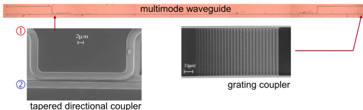
multimode waveguide
grating coupler
tapered directional coupler
Fig. 2. Microscope pictures of the 4-mm long 2-mode SOI waveguide with details of the directional coupler mode (de)multiplexer and the grating coupler used to couple the chip to standard single-mode fibers.
Mode-selective wavelength conversion was realized as an example of all-optical signal processing [11]. A 4-mm
long multimode bus waveguide supporting the TE0 and TE1 modes and equipped with a pair of mode
(de)multiplexers was fabricated, as shown in Fig. 2. Strong four-wave mixing (FWM) occurs when the pump and signal light are on the same spatial mode, while weak FWM is obtained between different modes as a result of phase mismatch. The idler due to inter-mode FWM is suppressed by more than 20 dB compared to the idler resulting from the interaction of pump and signal on the same spatial mode. The converted idler is extracted from the nonlinear waveguide thanks to a mode demultiplexer.
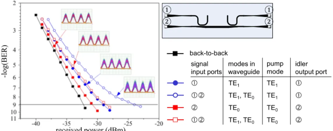
② ① ② ① -lo g( BE R ) received power (dBm) back-to-back signal
input ports modes inwaveguide pumpmode idleroutput port
TE1 TE1 TE1, TE0 TE1 TE0 TE0 TE1, TE0 TE0
Fig. 3. BER characterization of mode-selective wavelength conversion.
The good selectivity of the process enables its dynamic characterization with modulated signals. The pump light was modulated at 40 Gbit/s in the return-to-zero format while the mode-multiplexed signals were continuous waves. Wavelength converted modulated signals are obtained on one or the other mode depending on the choice of the mode on which the pump wave is coupled. The results of bit-error-ratio (BER) characterizations are reported in Fig. 3, where the influence of the modal crosstalk is assessed. Improvement in multiplexer design and fabrication is expected to allow a reduction of the modal crosstalk.
4. Conclusion
The motivations behind the investigation of on-chip all-optical signal processing have been reviewed. Mode-selective wavelength conversion has been demonstrated at 40 Gbit/s in a silicon-on-insulator waveguide supporting two spatial modes. Other signal processing functionalities are under investigation.
Acknowledgments
This work was supported by the Danish Council for Technology and Production Science (10-093299), the Danish Council for Independent Research (DFF-1337-00152 and DFF-1335-00771) and Villum Fonden (NATEC Centre). Support from the Labex CominLabs (French National Research Agency program “Investing for the Future” ANR-10-LABX-07-01) is also acknowledged.
4. References
[1] D. J. Richardson, J. M. Fini, and L. E. Nelson, “Space-division multiplexing in optical fibres,” Nature Photon. 7, 354-362 (2013).
[2] Y. Chen et al., “41.6 Tbit/s C-Band SDM OFDM transmission through 12 spatial and polarization modes over 74.17 km few mode fiber,” J. Lightwave Technol. 33, 1440-1444 (2015).
[3] N. K. Fontaine et al., “Heterogeneous space-division multiplexing and joint wavelength switching demonstration," in Optical Fiber Communication Conference 2015, Post Deadline Papers, paper Th5C.5.
[4] S. Mumtaz, R.-J. Essiambre, and G. P. Agrawal, “Nonlinear propagation in multimode and multicore fibers: generalization of the Manakov equations,” J. Lightwave Technol. 31, 398-406 (2013).
[5] A. W. Poon, X. Luo, F. Xu, and H. Chen, “Cascaded microresonator-based matrix switch for silicon on-chip optical interconnection,” Proc. IEEE 97, 1216-1238 (2009).
[6] E. Narevicius, R. Narevich, Y. Berlatzky, I. Shtrichman, G. Rosenblum, and I. Vorobeichik, “Adiabatic mode multiplexer for evanescent-coupling-insensitive optical switching,” Opt. Lett. 30, 3362-3364 (2005).
[7] M. Greenberg and M. Orenstein, “Multimode add-drop multiplexing by adiabatic linearly tapered coupling,” Opt. Express 13, 9381-9387 (2005).
[8] Y. Ding, J. Xu, F. Da Ros, B. Huang, H. Ou, and C. Peucheret, “On-chip two-mode division multiplexing using tapered directional coupler-based mode multiplexer and demultiplexer,” Opt. Express 21, 10376-10382 (2013).
[9] J. Wang, S. He, and D. Dai, “On-chip silicon 8-channel hybrid (de)multiplexer enabling simultaneous mode- and polarization-division-multiplexing,” Laser Photonics Rev. 8, L18-L22 (2014).
[10] L.-W. Luo, N. Ophir, C. P. Chen, L. H. Gabrielli, C. B. Poitras, K. Bergman, and M. Lipson, “WDM-compatible mode-division multiplexing on a silicon chip,” Nature Commun. 5, 3069 (2014).
[11] Y. Ding, J. Xu, H. Ou, and C. Peucheret, “Mode-selective wavelength conversion based on four-wave mixing in a multimode silicon waveguide,” Opt. Express 22, 127-135 (2014).