O
pen
A
rchive
T
OULOUSE
A
rchive
O
uverte (
OATAO
)
OATAO is an open access repository that collects the work of Toulouse researchers and
makes it freely available over the web where possible.
This is an author-deposited version published in :
http://oatao.univ-toulouse.fr/
Eprints ID : 18259
To link to this article :
DOI: 10.1109/EMCCompo.2017.7998105
URL : http://dx.doi.org/10.1109/EMCCompo.2017.7998105
To cite this version :
Serpaud, Sébastien and Ghfiri, Chaimae and Boyer,
Alexandre Proposal for combined conducted and radiated emission
modeling for Integrated Circuit. (2017) In: EMC Compo 2017 (The 11th
International Workshop on the Electromagnetic Compatibility of Integrated
Circuits), 4 July 2017 - 8 July 2017 (Saint Petersburg, Russian Federation).
Any correspondence concerning this service should be sent to the repository
administrator:
[email protected]
Proposal for combined conducted and radiated
emission modelling for Integrated Circuit
S. Serpaud
1,2, C. Ghfiri
1,3(1) IRT Saint-Exupéry, 118 route de Narbonne, F-31432, Toulouse, France
[email protected] [email protected]
(2) Nexio, 48, Rue René Sentenac - 31300 Toulouse, France
A. Boyer
1, A Durier
(3) CNRS, LAAS, 7 avenue du colonel Roche, F-31400 Toulouse, France
(4) Univ. de Toulouse, INSA, LAAS, F-31400 Toulouse, France
Abstract — This paper describes a methodology to build a
combined conducted and radiated emission model for integrated circuits. The development of emission models of a FPGA extracted from two different approaches is presented and discussed. The first approach allows to build a predictable model from FPGA implementation and some passive measurement on FPGA device. The second approach allows to build a model from only the near field measurement. In conclusion, the accuracy of both models as well as the advantages and disadvantages are discussed.
Keywords — Integrated circuit; modelling; ICEM; conducted; radiated; emission; FPGA; Near field.
I. INTRODUCTION
Several standards exist to build Electro Magnetic Compatibility (EMC) or Signal Integrity (SI) model. The Input output Buffer Information Specification (IBIS) model used for SI modelling mainly describes Integrated Circuit (IC) time-domain output behaviour. The Integrated Circuit Immunity Model (ICIM) and the Integrated Circuit Emission Model (ICEM) proposed by the IEC62433 standard describe respectively the IC immunity and the IC emission behaviour in frequency domain. So for each EMC issue exists an IC EMC model, each with its own extraction method and format.
Given the complexity of the new IC generation, the development of several models is not compatible with industrial constraints. We propose in this paper a methodology to build a combined model to describe both the conducted and radiated emission behaviour of complex device. This approach will be compared to the extraction method from IEC61967-3 - Near Field Scan Emission (NFSE) [1] measurements suggested by IEC 62433-3 - ICEM-Radiated Emission standard [2]. As conclusion, a discussion will be started on the compared advantages and disadvantages of each method.
II. NEAR FIELD MEASUREMENT OF THE DEVICE UNDER
TEST
For this study, we have selected a Field Programmable Gate Array (FPGA) to demonstrate the proposed approaches ability to model complex IC radiated emission (RE). The
studied IC is a XILINX Spartan 6 providing 9152 configurable logic blocks and up to 186 user IOs divided in 4 banks with separated power supplies. The Spartan 6 is packaged into a fine pitch Ball Grid Array (BGA) 256-balls package (see Fig. 8 and Fig. 9). The FPGA is clocked by an external 16 MHz quartz oscillator connected to the T8 input. The NFSE measurements have been performed for six FPGA configurations as described by Table I. The activity rate, i.e. the number of internal resources used in the FPGA, and the number of switching IOs are considered as variable to analyse their respective contribution to the near-field radiation.
TABLE I. PROGRAMM CONFIGURATION OF FPGA DEVICE
Activity rate
Configurations
With periodical switching of two
I/Os at 8 MHz (T9 and C16) Without IOs switching
20 % “Config 20% IOon” “Config 20% IOoff”
40 % “Config 40% IOon” “Config 40% IOoff”
90 % “Config 90% IOon” “Config 90% IOoff”
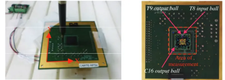
Fig. 1 presents the test board. The measurement frequencies start at 5 MHz and go up to 1.8 GHz. Two types of magnetic field probe are used: one for the Hx and Hy component and another for the Hz component. The spatial resolution of the probes is 0.5 mm. They have been calibrated according to the methodology presented in the IEC TS 61967-3 A-Annex [1]. The signal captured by the probe is amplified by a 40dB low-noise amplifier and measured by a FSP R&S receiver. The probes are moved by a 3D scanner system at 2.5 mm above the top Printed Circuit Board (PCB) surface (1.1 mm above the top of FPGA package). All the equipments are controlled by BAT-Scan software from Nexio.
Fig. 1. Near Field measurement on FPGA board
Area of measurement X Y T9 output ball C16 output ball T8 input ball
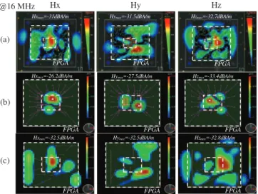
Fig. 2. Measurement of Hz component with configuration “Config 90% IOon”
Fig. 3. Measurement of Hz component with configurations: a) “Config 40% IOon” b) “Config 20% IOon” c) “Config 90% IOon” at 72 MHz (vector)
Fig. 4. Measurements of Hz component of FPGA core activity with configurations: a) “Config 90% IOon”, b) “Config 20% IOon”
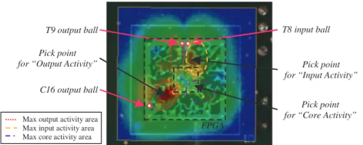
We present in this paper only the most relevant information to illustrate our study. Figs 2 to 4 present the normal magnetic field (Hz) maps measured with different FPGA configurations at several frequencies. Three different activity areas are clearly visible on the near-field maps as illustrated by Fig. 5. The first area is above the input T8 and is related to the current that circulates along the input pin connected to the external oscillator. This activity is weak and often masked by other activities, but it has a high frequency spectral content. The second area is due to the internal core activity of FPGA as shown by Fig. 4. The core activity is visible on I/O connections and their power delivery banks: the bank 1 for C16_out I/O and the bank 2 for T8_clk and T9_out IOs. These two first areas produce emission at 16 MHz harmonic frequencies. The last area emission as shown by Fig. 2 and Fig. 3 is visible on the FPGA bottom left corner due to the C16 I/O switching and on the FPGA centre top due to the T9 I/O switching. It produces a significantly high emission at 8 MHz and its odd harmonics up to several hundreds of MHz.
The core activity emission is visible up to 100 MHz. Above this frequency, only the I/O activity is visible. Obviously, the magnitude of radiated emission due to the core activity is related to the activity rate. The comparison between the near-field maps obtained with the different FPGA
configurations presented in Fig. 4 shows a 3 dB attenuation between each configuration. A 6 dB attenuation is visible between the low (20%) and the high (90%) activity rate. The near-field emission produced by the I/O activity is not affected by the activity rate used in the FPGA core, as shown in Fig. 2 and Fig. 3. This activity depends only of the internal I/O driver characteristic and the external load connected to the I/O on the Printed Circuit Board (PCB).
Fig. 5. Localization of magnetic field maxima at 0.6 mm above the FPGA package surface
This information is very important to guide the development of the ICEM model. In the next paragraph, we will describe how to build an ICEM-RE model of FPGA following two different approaches.
Pick point
for “Output Activity” Pick point
for “Input Activity”
Pick point for “Core Activity” T9 output ball
C16 output ball
T8 input ball
Max output activity area Max input activity area Max core activity area
FPGA F = 2*F0 = 16MHz F = 4*F0 = 32MHz F = 6*F0 = 48MHz F = 8*F0 = 64MHz F =10*F0 = 80MHz F = 11*F0 = 88MHz F =11*F0 = 88MHz a) FPGA FPGA X Y b) Magnitude Phase FPGA FPGA c)
Hzmax=-23.2dBA/m Hzmax=-23.4dBA/m Hzmax=-23.9dBA/m
b)
FPGA FPGA
FPGA FPGA
Hzmax=-30.9dBA/m Hzmax=-35.5dBA/m Hzmax=-36.5dBA/m Hzmax=-35.2dBA/m Hzmax=-31.6dBA/m
a)
FPGA FPGA FPGA
FPGA FPGA
Hzmax=-22.2dBA/m Hzmax=-25.4dBA/m Hzmax=-30.1dBA/m Hzmax=-30.2dBA/m Hzmax=-25.7dBA/m
F = F0 = 8MHz F = 3*F0 = 24MHz F = 11*F0 = 88MHz FPGA FPGA FPGA F = 202*F0 = 1616MHz FPGA F = 46*F0 = 368MHz FPGA
Hzmax=-22.2dBA/m Hzmax=-24.8dBA/m Hzmax=-23.1dBA/m Hzmax=-25.9dBA/m Hzmax=-56.8dBA/m
III. ICEM-RE MODEL
The conducted emission of an integrated circuit can be modelled according to the IEC 62433-2 Integrated Circuit Emission Model for Conducted Emission (ICEM-CE) approach, standardized as IEC 62433-2 [3]. ICEM-CE proposes a generic model topology based on two main blocks.
The Passive Distribution Network block (PDN) describes the propagation path of the transient current produced by the on-chip switching activity to outside the device. It consists of a passive element network often constructed from S-parameter measurements [6].
The Internal Activity block (IA) describes all IC’s noise sources as the digital core, the analogue function and the I/O buffers. It typically consists of current sources modelling the different contributors to the internal activity of the IC. The
noise produced by the IOs switching is called IAIO and can be
modelled accurately using the IBIS model as described in [4]. The noise produced by the digital core is called IACORE. A method to extract it for XILINX Spartan 6 is described in [5].
The IEC-62433-3 ICEM-RE [7] [3] proposes a model topology based on a dipoles network extracted from NFSE measurements. With this approach, the radiated emissions can be extrapolated accurately at any farther distance from the IC. However, this model is completely separated from ICEM-CE model and is only representative of the IC configuration used during the NFSE measurement. The effect of a configuration change, external load change or filtering change cannot be predicted with the type of model.
In this paper, we propose to build a common IC model for both conducted and radiated emission simulation. The originality of the proposal is to build ICEM-RE model from ICEM-CE model. We proposed to add a new block to model the radiated emission into the ICEM-CE model as described in Fig. 6. The Equivalent Antenna Network (EAN) block is connected to the PDN block. The EAN includes several wire networks modelling the RE of IC due to the physical package structure. All these equivalent dipoles are excited by the current predicted by ICEM-CE model. The combined model is available to predict both near and far field emission of IC.
Fig. 6. Structure of ICEM-RE model from ICEM-CE
In the following parts, we present two approaches for ICEM-RE model construction. A final chapter discuses about the advantage and disadvantage of each proposed approach. A. Approach 1 : ICEM-RE model from ICEM-CE
In this approach the ICEM-CE model is reused to build the ICEM-RE model. The EAN block is added to model the radiated emission from the package interconnects. We made
the assumption that the IC package covers a larger surface area than the die. Thereby the radiated emission of the die can be neglected. All power and I/O interconnects network are modelled by thin wires. The current simulated by the ICEM-CE model is injected on each wire of the EAN block. The next paragraphs describe the approaches to extract all parts (IA, PDN and EAN) of this combined ICEM-CE/ICEM-RE model.
1) IA and PDN block extraction
The IACORE block models the noise produced by the
switching of the active logic blocks. As described in [5], it consists of a set of current sources based on canonical waveform (e.g. triangular pulse). The magnitude I0 and the duration ! of the pulse can be calculated when the dynamic power consumption, the toggle rate and the data path delay are known. Using the Xilinx synthesis tools of, these parameters
are estimated, and the characteristics of the IACORE equivalent
current sources could be deduced for the different FPGA configurations. The core activity is modelled by two current sources: one for the configurable logic block switching, the other for the clock tree.
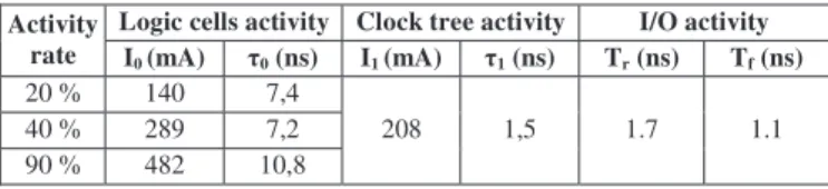
The same methodology could be used to extract equivalent current sources that models I/O switching activity. However, the IBIS model provided by the IC manufacturer offers a good accurate method to simulate the conducted noise produced by I/O switching. The power supply terminals of buffer models are connected to the PDN block of ICEM model. All estimated parameters of IA as presented in the Table II according to different configurations (activity rate) of the FPGA core.
TABLE II. ESTIMATED PARAMETERS OF IA CORE BLOCK
Activity rate
Logic cells activity Clock tree activity I/O activity
I0 (mA) !0 (ns) I1 (mA) !1 (ns) Tr (ns) Tf (ns)
20 % 140 7,4
208 1,5 1.7 1.1
40 % 289 7,2
90 % 482 10,8
The PDN block models the propagation path of current from IA generator, on the die, to the PCB. Several papers such as [4], [5] or [6] describe how to extract PDN model from S-Parameters measurements. This N-Port passive element model could be converted into Spice model or kept in Touchstone Touchstone format according used electrical circuit simulator. In this paper, we reused IA and PDN models developed in [5].
2) EAN block extraction from package layout of device Following our assumption, the package interconnects are the main contributors of IC RE. The EAN block constitute a set of small antennas excited by the transient current produced by IC core and I/O switching activities. The prediction of IC RE relies on the knowledge of the position of these antennas and the currents that excite them. The currents which flow along package interconnects can be simulated precisely from ICEM-CE model when these interconnects are modelled by an electrical model (e.g. lumped RLC circuit). Moreover, from an accurate geometrical model of the IC package, geometrical positions can be assigned to these interconnects, constituting the antennas network. With the assignation of these geometrical coordinates, an ICEM-RE model can be constructed from ICEM-CE model.
ICEM-CE
IA
Load PCB PDN
ICEM-RE
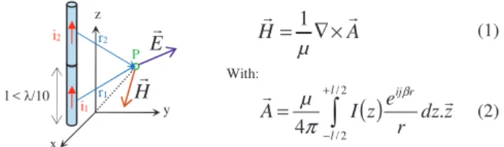
A simple method to compute the electric and magnetic fields radiated by package interconnects is based on the thin wire approximation as described by Fig. 7. Each interconnect is meshed into small elementary thin wires crossed by a current “I” that is supposed constant along the wire. This assumption remains valid until the interconnect length l is electrically short (l < "/10). The magnetic fields generated by each elementary wire oriented along z axis are calculated according to (1), where r is the distance to the observation point. If the package interconnect is longer than "/10, it is split into elementary dipoles. The total magnetic field at the observation point is the sum of the contribution of all elementary dipoles.
Fig. 7. Thin wire approximation for calculation of near-field emission from package interconnects
As described in Fig. 8, BGA package includes a build-up laminate substrate to route all die pads to the specific ball. This build-up laminate substrate is composed of traces, via and ground/power planes.
Fig. 8. Two-layer plastic BGA package
For reliability study, X-ray inspection is used to analyse the internal structure of IC packages. Fig. 9 shows the X-rays measurement of the FPGA. From the X-Ray inspection and the knowledge of the FPGA pinout, it is possible to build the physical PDN structure, identify the pins type and finally associate each wire of EAN to an electrical element of the ICEM-CE model.
The Fig. 10 shows all the FPGA power supply connections. The T8_clk, T9_out and C16_out connections are marked in pink. The EAN block model built from this approach is presented in Fig. 14(a).
Fig. 9. 3D X-Ray view of FPGA (Spartan 6 family of Xilinx)
Fig. 10. PDN structure of FPGA (Spartan 6 family of Xilinx)
3) EAN block extraction from IC pinout
This EAN structure extraction method is relevant for simple package. In example, for QFP package where all connections can be defined as a wire starting from the middle of IC (the die) to the periphery of IC (the pad). Coupled with the pinout of device, building the structure of the EAN is not a complex task. One wire is used to connect all balls with position of die pad for each interconnect which is taken into account. The EAN block model built from this approach is presented in Fig. 14(b).
B. Approach 2 : ICEM-RE model from NFSE measurements In this approach the ICEM-RE model is extracted from NFSE measurement in vector. The phase of radiated emission is added to improve accuracy of model. The IA block is built around several current generators modelling the different internal FPGA activity. The PDN block is not used in this approach. The EAN block of the model consists in several wires excited by IA generators. The complete extraction method is defined in following.
1) IA block extraction from NFSE measurements
The NFSE measurement analysis allows to extract IA parameters. Fig. 12 shows emission spectra of internal activities according to the activity rate. Their RE spectra for each activity rate are picked in points marked in Fig. 5. The shape of the measured spectra is typical of periodic trapezoidal pulse spectral envelop as presented in Fig. 11. The transient parameters of each internal activities sources can be estimated from the measured spectral envelop. The magnitude of each generator could be extracted from the tangential magnetic field value measured for each activity using Equation 4. The TABLE III. resumes all IA block parameters extracted from NFSE measurements.
Fig. 11. Relation between trapezoidal pulse waveform in time domain and the envelop of its spectrum in frequency domain
! " # $ % & π t A . 2 log 20 !! " # $$ % & = 1 0 . . . 2 log 20 c t f F F A A π !! " # $$ % & 2 0 . . . 2 log 20 c t F F A π r c T F . 1 2=π
Periodic Trapezoidal Pulse:
0 Tr Tf Ton T Toff Tr on c T F . 1 1 π = t A Freq 0 Magnitude -20dB/decade -40dB/decade Magnitude in dB Top Bottom Die
Au Bond Wire Epoxy Overmold
Top Copper
BT/FR5 core
Bottom Copper Solder ball
Top Bottom Vcc0_Bank1 Vcc0_Bank0 Vcc0_Bank3 T9_out T8_clk C16_out Vcc0_Bank2 Die A µ H ! ! × ∇ =1
( )
'
+ − = 2 / 2 / . 4 l l r ij z dz r e z I µ A ! ! β π With: (1) (2) l < "/10 r2 r1 H ! E ! P i2 i1 z y x Top of Die Top of substrate Top of FPGA 0.65 Top of PCB 1.15 1.4 0 Dimension in mmFig. 12. Internal activities : measurement (HZ) vs activity rate of device
TABLE III. ESTIMATED PARAMETERS OF IA CORE BLOCK EXTRACTED FROM NFSE MEASUREMENT
Activity type
Frequency domain parameters Time domain parameters
|Htang|max [dBµA/m] |Af|max* [mA] F0 [MHz] Fc1 [MHz] Fc2 [MHz] |At|max [mA] T [ns] Ton [ns] Tr [ns] Core90% 98.5 1.1 16 20 80 10.6 62.5 15.9 3.2 Core40% 92.8 0.564 5.5 Core20% 89.1 0.368 3.6 Input 87.6 0.310 16 310 550 9.7 62.5 1 0.58 Output 97.8 1 8 200 280 39.2 125 1.6 1.15
* Value compute from equation (4) with h=1.15mm; t=50µm; R1=2.5mm
2) EAN block extraction from NFSE measurements
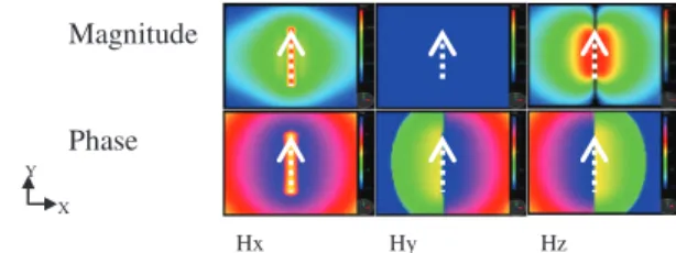
The analysis of the near-field measurements shows information that can be used to build EAN from wire elements. Fig. 13 shows vector radiated emission of wire (one dipole) for each Hx, Hy and Hz components. One dipole has a specific magnitude signature. The position of an isolated dipole can be localized with high precision from the Hz magnitude component. Coupling with the Hx and Hy components, the magnetic signature of a dipole can be an help to build the EAN block. Phase is also a valuable information to localize the position and orientation of each dipole. As shown in Fig. 13, the position of dipole is marked by a high variation of the H-field phase (±#). The sign of this variation defines the dipole orientation. With this information, the analysis of near field measurement can help to build the EAN block. Fig. 3(c) shows the Hz near field (magnitude and phase) for “Config 90% IOon” configuration measured at 72 MHz where two wires are clearly identified according the previous information. The EAN block model built from this approach is presented in Fig. 14(c).
Fig. 13. wire simulation – Hx, Hy and Hz components in magnitude and phase
IV. SUMMARY ABOUT BOTH ICEM-RE EXTRACTION APPROACHES
We have described two different approaches to extract ICEM-RE model. The complexity level of obtained models is different. As presented in Fig. 14, the EAN block of the full model extracted from the Approach 1 (“model 1”) contains 235 dipoles where the EAN block of full model extracted from Approach 2 (“model 2”) contains only 17 dipoles. The Fig. 15 present the “model 1” which described, with great precision, package and die of the device in SPICE format with IC-EMC software [8]. The “model 2” is a behavioural model resumed by the EAN block and activity generators.
Fig. 14. EAN block models extracted - (a) from X-Ray of package; (b) from pinout of device; (c) from NFSE measurement
Fig. 15. ICEM-RE Model obtained from Approach 1 on IC-EMC software [8]
Regarding the H-field emission produced by the C16 output buffer switching (Fig. 16), all models give a good prediction of the radiated emission at 8 MHz. Simulations provide a correct prediction of the maximum and the overall distribution of the H-field. About the core activity radiation (Fig. 17), the model, extracted following the Approach 2 from NFSE measurement, gives a correct prediction. With the model extracted following the Approach 1 from ICEM-CE model, the prediction is less satisfying. The overall distribution of the H-field is not correct. However, this one could be improved by using the EAN block extracted from X-Ray of package (not presented in this paper due to current IC-EMC software limitation in terms of maximum number of radiated dipoles), but at the price of a larger number of dipoles to model exactly the complex power distribution network of the package. If we observe the H-field maximum, for a
Phase X Y Magnitude Board model PDN FPGA 1 ! probe IA FPGA C16 output buffer T9 output buffer PCB trace + Load PCB trace + Load @IC-EMC software 2017 (a) (b) (c) 17 radiated dipoles 115 radiated dipoles 235 radiated dipoles (3) ! " !"#$ #$%&'()*+,'-. % % / 01,2-)3&$$-'" / !4 λ << << <<h t R handR t Assume ; , : (4) ( ) () * +, -+ + + = h t h t R R H I 2 2 . 2π tan ( )() * + , -+ + + = h t R R h t I H 2 2 2 tan π Hx Hy Hz Ainput = 87.6dBµ A/m Frequency &' ('& )' *' +' ,' M ag n it u d e d B µ A /m Fc1out Fc2out “Config 90% IOon” Hz “Config 40% IOon” Hz “Config 20% Ioon” Hz
Contribution of “core Activity” Inputs activity
Fc2core Fc1core
Acore_90% = 98.5dBµ A/m
Acore_40% = 92.8dBµ A/m Contribution of “IO Activity”
&' ('& )' *' +' ,' M ag n it u d e d B µ A /m Frequency Acore_20% = 89.1dBµ A/m “Config 90% IOon” Hz “Config 40% IOon” Hz “Config 20% Ioon” Hz Core activity Fc1out Fc2out Aoutput = 97.8dBµA/m Frequency &' ('& )' *' +' ,' M ag n it u d e d B µ A /m “Config 90% IOon” Hz “Config 40% IOon” Hz “Config 20% Ioon” Hz Outputs activity
predictive approach, we can conclude that the prediction is good. For improve accuracy prediction of the core activity radiation, it is necessary to have a more accurate model of the PDN at the IC level. The limit of the method using radiated dipoles network is reached with this device. The use of a 3D simulation tool becomes necessary for finely modeling the complex IC package.
Fig. 16. Comparaison betwween NFSE Measurements (Config 90% IOon) (a) vs simulation results of the FPGA model following Approach 1 - From ICEM-CE with EAN block extracted from X-Ray of package (b) or from pinout of device (c) and following Approach 2 - From NFSE measurement (d).
Fig. 17. Comparaison betwween NFSE Measurements (Config 90% IOoff) (a) vs simulation result of the FPGA model following Approach 1 - From ICEM-CE with EAN block extraction from pinout of device (b) and following Approach 2 - From NFSE measurement (c).
V. CONCLUSION
This paper has described two methodologies to build a radiated emission model for a complex integrated circuits. The first model very precisely describes the structure of device.
Information from FPGA design tool, S-parameters
measurements and the X-ray inspection provide valuable information to build the structure of the model. No final application board is necessary to build a predictive model for various implementation of FPGA device. This approach is relevant to anticipate the EMC issues. However this approach requires huge work and time and is currently limited at the Xilinx FPGA device family. Note that this model defined in SPICE format allows working at board level to optimize the design (e.g. signal integrity or decoupling capacitor network optimization) from predictive numerical model of IC taking into account the specific user application behaviour even before the first run of application boards. The second approach based on NFSE measurement gives a simpler model. This model can be quickly built from NFSE measurement on application board. Compared to the first approach, this one includes all unknowns relative to the application board fabrication process. But this approach needs a prototype to perform NFSE measurement and is limited at one specific IC configuration.
Both approaches can be used to evaluate radiated emission in far field to improve EMC at system level. In Summary, both approaches are complementary and are able to answer to a large part of the EMC issues requiring the use of IC model.
!"#$%&'()*+($,-This work is supported by the IRT Saint-Exupery’s Electronics Robustness project sponsored by Airbus
Operations, Airbus Group Innovations, Continental
Automotive France, Hirex Engineering, Nexio, Safran Electrical & Power, Thales Alenia Space France, Thales Avionics and the French National Agency for Research (ANR). The authors would also thank Continental Automotive France Qualification Laboratories at Toulouse for FPGA X-Ray views.
.(/(0($"(1-[1] IEC61967-3 Integrated circuits - Measurement of electromagnetic emissions - Part 3: Measurement of radiated emissions - Surface scan method- Edition 1.0, 2014, IEC
[2] IEC62433-3: EMC IC modelling – Part 3: Models of integrated circuits for EMI behavioural simulation – Radiated emissions modelling (ICEM-RE) - Edition 1.0, January 2017, IEC.
[3] IEC62433-2 - EMC IC modelling – Part 2: Models of integrated circuits for EMI behavioural simulation – Conducted emissions modelling (ICEM-CE) - Edition 2.0, January 2017, IEC.
[4] C. Ghfiri, A. Durier, A. Boyer, S. Ben Dhia, C.Marot “Construction of a Integrated Circuit emission model of a FPGA” APEMC 2016, Shenzhen, China
[5] C. Ghfiri, A. Durier, A. Boyer, S. Ben Dhia, “Methodology of modelling of the internal activity of a FPGA for conducted emission prediction purpose”, submitted at EMC Compo 2017, St petersburg, Russia [6] S. Serpaud, J. L. Levant, Y. Poiré, M. Meyer, S. Tran, "ICEM-CE
extraction methodology", EMC Compo 2009, Nov. 17-19, 2009, Toulouse, France.
[7] Abhishek Ramanujan, Frederic Lafon, Priscila Fernandez-Lopez; “Radiated Emissions Modelling From Near-Field Data – Toward International Standards”, APEMC 2015, Taipei – Taiwan.
[8] E. Sicard, A. Boyer IC-EMC v2.5 User's Manual, Oct. 2011, 260 pp, ISBN 978-2-87649061-1, www.ic-emc.org.
(a) @16 MHz
Hxmax=-31dBA/m
FPGA
Hymax=-31.5dBA/m Hzmax=-32.7dBA/m
Hx Hy Hz
FPGA Hxmax=-32.5dBA/m
FPGA
Hymax=-32.5dBA/m Hzmax=-32.8dBA/m
(c) FPGA Hxmax=-26.2dBA/m FPGA Hymax=-27.5dBA/m FPGA Hzmax=-33.4dBA/m FPGA FPGA (b) FPGA @8 MHz FPGA Hxmax=-26.7dBA/m Hxmax=-23.7dBA/m FPGA Hymax=-22.4dBA/m Hymax=-19.6dBA/m FPGA Hzmax=-25.7dBA/m Hzmax=-22.4dBA/m Hx Hy Hz (a) (b) (c) (d)
Hxmax=-24.5dBA/m Hymax=-24.5dBA/m Hzmax=-22.6dBA/m
FPGA FPGA FPGA
FPGA
FPGA FPGA
FPGA FPGA FPGA