OATAO is an open access repository that collects the work of Toulouse
researchers and makes it freely available over the web where possible
Any correspondence concerning this service should be sent
to the repository administrator:
[email protected]
This is an author’s version published in:
http://oatao.univ-toulouse.fr/25462
To cite this version:
Guerch, Kévin
and Paulmier, Thierry and Guillemet, Sophie
and Lenormand,
Pascal
Characterisation of charging kinetics of dielectrics under continuous
electron irradiation through real time electron emission collecting method. (2015)
Nuclear Instruments and Methods in Physics Research Section B: Beam
Interactions with Materials and Atoms, 349. 147-154. ISSN 0168-583X
Characterisation of charging kinetics of dielectrics under continuous
electron irradiation through real time electron emission collecting
method
Kévin Guerch
a,b,*,Thierry Paulmier
a,Sophie Guillemet-Fritsch
b,Pascal Lenormand
b • 0NERA, 2 Avenue Edouard Belin, 31055 Toulouse Cedex 4, Franceb OR/MAT -Jnstitut Carnot (CNRS) Université Paul Sabatier, 118 route de Narbonne, 31062 Toulouse Cedex 09, France
ARTICLE INFO ABSTR ACT
Keywords: Surface potential Electron emission Ionisation elfect Charging Dielectric
Dielectric materials used for spacecraft applications are often characterised under electron irradiation in order to study their physical and electrical rnechanisms. For surface potential measurement, a small rernovable fiat device based on the secondary electron spectrometer method has been developed and installed in the CEDRE irradiation test facility at ONERA (Toulouse, France). This technique was developed to get rid off specific issues inherent to the Kelvin Probe technique. This experimental device named REPA (Repulsive Electron Potential Analyser) allows in situ and real time assessment of the surface potential built up on dielectric materials under continuous electron irradiation. A calibration has been perforrned in order to validate this experimental setup. Furthermore, to optimise its efficiency, the physical beha viour of this device has been modelled and numerically simulated using Particle In Cell ( PIC) model and a dedicated nurnerical code called SPIS (Spacecraft Plasma Interactions System). In a final step, elec trical characterisations of a charged dielectric have been carried out under continuous electron irra diation with this new method. These results have been compared with measurements perforrned in same experirnental conditions with conventional Kelvin Probe method. The experimental results have been discussed in this paper. To conclude, advantages of this experirnental setup in regard of this appli cation will be emphasised.
1. Introduction
In space conditions, dielectric materials, used on spacecraft, have to cope with strong electron radiation levels that may lead to strong charging and discharging hazards as well as material degradation and the alteration of their physical properties. Accurate electrical characterisations and the use of dedicated experimental techniques are of high importance for thorough extraction of the electric properties of the material. One of the main issues is the measurement of electric potential built up at the dielectric surface by electron radiation. The use of conventional measurement techniques such as non contact Kelvin Probe (KP) method [ 1 3] can become insufficient and inconvenient if the test ed dielectric material presents a large electric conductivity. During the KP procedure, the electron beam is indeed switched off by the probe during measurement. This process may cause a significant
*
Corresponding author at: ONERA, 2 Avenue Edouard Belin, 3 1055 Toulouse Cedex 4, France.E-mail address: [email protected] (K. Guerch). http://doi .org/10. 1016/j.nimb2015 .02.046
relaxation of charges. Moreover, the low measurement frequency of this technique may also result in an underestimated measure of the surface potential.
This paper describes the development, operation and optimisa tion of a new measurement device called REPA (Repulsive Electron Potential Analyser) and devised at DESP (ONERA Toulouse, France) to characterise the charging kinetics of dielectrics under con tinuous electron radiation in a vacuum test chamber. The principle of this experimental deviœ is based on secondary electron (SE) spectrometer method [4,5]. Severa) kinds of detector based on this method have been designed and used since many years and espe cially in the Scanning Electron Microscope (SEM). Secondary elec tron spectrometers allow studying the secondary electron yield (SEY) of materials. Sorne spectrometers operate by electrostatic detlection and others by retarding field. The second kind of spec trometers is commonly called Retarding Field Analyser (RFA) [6]
and its operating principle is similar to the REPA method. Their geometry is often hemispherical but the design, the biasing of grids and their distance between them vary from one device to another
have likewise been adapted especially in SEM in order to investi gate the quantitative voltage contrast of specimens or Integrated Circuits (IC) [8). Indeed, some devices operate by using radial elec trostatic deflection fields [9,10) and others are based on pre accel eration and retarding fields [11,12). Other physicists have developed and optimised this kind of experimental setup with grids, named RPA (Retarding Potential Analyser) that allows deter mining ions energy [13).
Different spectrometers have therefore been used in several application domains since the first development of this analytic method. Thus, this paper explains the adaptation and the optimisa tion of such device that allows determining the evolution of sur face potential of irradiated dielectrics over continuous radiation time. This new apparatus is non hemispherical, small and easily removable. A calibration process has been performed in order to validate both the measurement method and the developed proto type. The calibration process is described in this paper. For the development of this kind of equipment, it is important to consider the geometrical parameters such as space between the grids or the influence of their biasing. Thus, numerical simulations (PIC model) have been performed in order to understand the electrostatic con figuration of this experimental setup in operation and ultimately optimise it. Consequently, we detail the adopted development approach as well as the different numerical tests performed with the SPIS software (Spacecraft Plasma Interactions System [14)). Experimental validation tests have then been carried out on glass samples with both measurement techniques: Kelvin Probe and REPA methods.
2. Experimental set-up and method
2.1. Overview of irradiation test chamber (CEDRE)
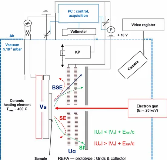
The CEDRE faàlity is one of the many high vacuum electron irradiation test chambers localised at ONERA Toulouse. CEDRE means in French: "Chambre d'Etude De Revêtements Electrisés". In fact, this facility has the capability to be versatile and easily adjustable to characterise surface potential of electron irradiated dielectrics through several instruments (Fig. 1 ). Therefore, it is pos sible to assess the charging and discharging kinetics of spacecraft materials in space representative conditions. The vacuum level during tests is approximately equal to 5. 10-7 hPa. Chamber
vacuum pumping is performed thanks to a dry pump group in order to limit contamination An electron source is available to irradiate samples by controlling the flux and the energy of the elec tron beam. Another source such as a UV lamp can be easily installed if necessary. A ceramic heating element sustains the sam pie holder which can be whether floating or grounded. This experimental assembly developed at ONERA allows controlling the temperature in the range between 20 °C and 400 °C. The heat ing element can be used to assess the temperature influence on the conductivity. It also allows outgassing the samples before the irra diation tests. It has been used as well to discharge the samples after the irradiation test. The REPA instrument that is the focus of this paper is directly mounted on the sample holder. This assem bly is installed on one of four faces of a rotating cube. Other instru ments such as Faraday cups are installed on other cube faces. Thus,
PC : control, Air Vacuum 5.10·7 mbar Ceramic heating element Tmax ~400 C
Vs
Sample..
, acquisition' 1
=
Voltmeter KPBSE
/
_
.;;;;--�
, ::!" ...=
,✓: ... ... = I , , , I I + 18 VREPA - prototype : Grids & collecter
Video register
Electron gun (Ei < 20 keV)
�---·
Fig. 1. CEDRE instrumentation and experimental device principle (side view).the electron flux can quickly be measured before surface potential characterisations. A Kelvin Probe is installed in CEDRE to assess the charging and relaxation kinetics. A CCD camera is used to visually check some observable phenomena during tests. The used electron gun (Kimball, Mode) EGPS 42128) allows having reproduàble irra diation conditions. It provides a mono energetic electron beam (energy spread ::,,0.5 eV) with energy range between 1 keV and 20 keV and energy stability of ±0.01% during 1 h. Generally, the used beam is continuous and its flux ranges varies between
0.05 nA cm-2 and 100 nA cm-2.
Thus, the experimental method usually applied in CEDRE to study the charges transport in dielectrics is to implant incident electrons with calibrated flux and energy in order to measure the surface potential built up on the sample with a Kelvin Probe (KP Monroe Electronics Inc., Mode) 175, ±20 kV) [1). The continuous beam is focused (</J < 3 mm) or defocused (3 mm< <fJ < 50 mm, depending on the energy) in order to study the different conduc tion mechanisms (surface and bulk conductivityi lrradiated sam pies usually present surfaces greater than 20 mm x 20 mm and their distance to the KP is approximately equal to 3 mm in order to get a correct spatial resolution and to limit measurement uncer tainty. Data processing instruments, the Kelvin Probe and the Repulsive Electron Potential Analyser (REPA) are automatically controlled by computer using GPIB interfacing and a DAQ card under LabVIEW™ contrai.
2.2. REPA method and experimental setup
The REPA (Repulsive Electron Potential Analyser) allows mea suring dielectric charging kinetics under continuous irradiation. This devised method is based on the secondary electron spec troscopy method [4,5). Fig. 1 describes the method principle to measure the surface potentials (Vs) of a charged material. Samples irradiated under electron beam emit secondary electrons with very low energies (EsE) conventionally ranging from 0 to 50 eV [4). The secondary electron current (and backscattered elec trons) is measured through a collector installed behind two grids which have an applied bias voltage, noted Ug. lndeed, secondary electrons are accelerated and cross the grids before to be collected when IUgl is Jess than the sum of IVsl and E5iJq (q: elementary charge). The collector is biased at +18V with a stable battery in order to collect most secondary electrons coming from this collec tor itself ( due to secondary electrons impact ejected from sample ). Secondary electrons coming from the irradiated collector have
Applied U8
u �v
s_8
Fig. 2. Schematic curve of the collected current of SE (current threshold around V,) as a function of bias voltage applied to grids.
energy lower than this bias voltage [15). Consequently, this collec tor biasing allows avoiding secondary electron emission from the collector, leading then to an increase of the measured emission current. The biasing of collector at + 18 V increases the signal to noise ratio (by collecting SE from the collector when Ug <Vs+ EsEI q). Thus, the uncertainty decreases and the accuracy to detennine the surface potential of sample is improved.
The use of two grids biased with the same voltage ( Ug) allows getting a dense and homogeneous electronic barrier especially near their central hole. Thus, when grids voltage increases and becomes greater than the surface potential of the irradiated mate rial, the collected current signal steeply decreases. The electric field which accelerates the secondary electrons drops down and thus becomes too low for the emitted secondary electrons to cross the grids and reach the electron collector. When the grid voltage (Ug) varies from zero to its maximum value (higher than the surface
Electron beam axis
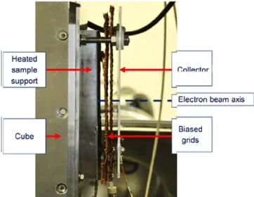
Biased grids
Fig. 3. REPA prototype (side view) installed in CEDRE.
Applied Ug (V) ·1000-900 ·800 ·700 ·600 ·500 ·400 ·300 ·200 ·100 0
r
�
-
---,
r
"
,.
"
'
1
-880 V -520 V -200 V -51 V 1 0 ·l ·2 .3 ·4 ·S ·6 .7 ·8 ·9 ---50 V ---200 V ---500 V ---850 V � ::,Fig. 4. Derivative current as a function of the applied potential grids for several surface poœntial on the biased metallic plate during its irradiation (20 keV, 1 nA cm-2, room temperature ).
Table 1
Calibration uncertainty for several biasing voltage as a function of the applied voltage gap àU bel'M!en two voltage set-points on the grid
Biasing (V) àU(V) Uncertainty (%)
-50 ±2
-200 ±<1
-500 5 ±4
-850 ±4
potential), the measured and collected eurrent steeply drops down when the grid voltage is equal to the sample surface potential (Fig. 2). The surface potential (Vs) can then be deduced from this eut off eurrent threshold. A computer code has been developed for contrai of grid biasing, eurrent measurement, scans frequency and number.
This experimental setup was designed and developed because the Kelvin Probe eut off the irradiation during the measurement. Furtherrnore, another benefit of this method versus the KP method is its higher measurement frequency. The measurement frequency of the REPA method is inversely proportional to the grid voltage scanning speed which allows determining the material surface potential. Typically, with amplitude of applied tension equal to 400 V and an applied voltage gap (.1.U) equal to 5 V, it is possible to perform one measurement every 15 s approximately versus 60 s for the KP method. However, this technique presents draw backs. The main one is the impossibility to characterise the relax ation kinetics of material contrary to the KP method. Indeed, this REPA method requires the collection of electrons emitted by the irradiated materials and can then only be applied during irra diation KP and REPA methods are therefore complementary for a thorough analysis of electric response of dielectric materials under irradiation.
2.3. Experimental validation on biased metallic plate 2.3.1. Experimental protocol
Fig. 3 shows the experimental configuration of the REPA proto type. We can observe on this picture the two grids ofthis prototype
Sample Experimental
device
device and the collector behind grids. The sample is installed on the heated sample support in front of the grids. The sample has to be installed in the same central axis as the device aperture and the electron gun axis in order for the electron beam irradiates the sample by coming through this measurement device.
2.3.2. Calibration
For calibration, a metallic brass plate has been used as sample, biased at given voltages (to simulate the charging potential) and irradiated with electrons. This sample was then biased at -50 V, -200 V, -500 V and -850 V. For each metal biasing, a potential scan was performed under electron radiation. Fig. 4 presents the derivative signal of the collected eurrent as a function of the grid voltage when different biasing voltages are applied on the metallic plate.
The position of each peak is in good agreement with the voltage applied to the metallic plate. Measurement uncertainties in per cent are presented in Table 1. We note that the voltage shift for -850 V and -500 V is greater than for -200 V and -50 V. This is mainly due to both instrumental and experimental issues. Firstly, the calibrations at -850 V and -500 V have been performed with a voltage supply which is different from the calibrations at -200 V and -50 V (respectively a Heinzinger 10,000 V and a Keithley 220 V). The uncertainty is linked to biasing controller con nected to the metallic calibration plate. The accuracy and the response time are better for the low voltage system. Secondly, an experimental error must also be considered. In fact, the uncertain ty mainly depends on the applied voltage gap .1.U during the mea surement. .1.U corresponds to the voltage step applied by the experimenter to perform measurement in defined voltage range (from Um;n to Urnax). The increase of this voltage step implies less
measure points which leads to stronger uncertainty on the current derivative and therefore to a reduœd aceuracy on the surface potential (but the measurement is faster). For -850 V and -500 V, .1.U is equal to 5 V (Table 1) and is greater than for
-200 V and -50 V (1 V). Consequently, the uncertainty is higher
for these two last potentials. The calibration measurements on the metal plate are reproducible.
3. Results and discussion
3.1. SPIS simulations for the validation and optimisation
ln order to understand the electrostatic configuration of the REPA system, SPIS Simulations have been performed [14). SPIS
[16,17) is a PIC mode! and allows evaluating the efficiency of device setup.
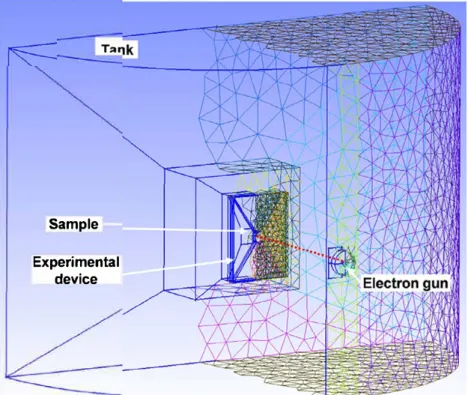
3.1.1. Modelling of the fadlity
The experimental setup has been designed with the software "Gmsh" that is a three dimensional finite element mesh generator
[18). The computer aided design of the CEDRE facility is shown in
Fig. S. For simplicity sake, we modelled half of the CEDRE facility with the electron gun to limit the volume mesh. Moreover, geome tries of REPA and sample support are simplified but these approximations do not influence electrostatic calculations. 3.1.2. SPIS simulations for the REPA optimisation
SPIS semi quantitative simulations have been performed on the one hand in order to understand the electrostatic configuration of this operating device and on the other hand in order to optimise it. Consequently, these simulations have been carried out with
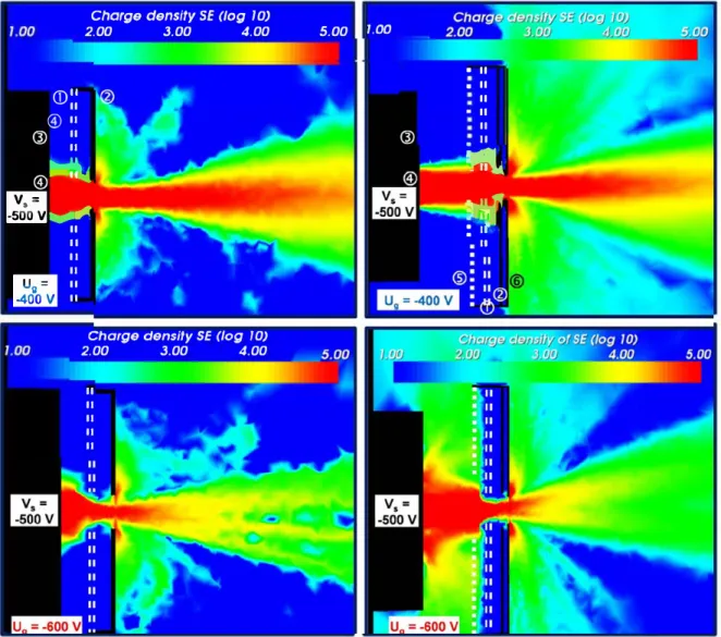
Charge density SE (log 10)
irradiation parameters matching the experimental ones. Thus, inci dent energy and current are respectively equal to 20 keV and 1 nAcm-2•
Fig. 6 allows emphasising the influence of electrostatic con figuration on the charge density of secondary electrons (SE) between the REPA prototype and the optimised deviœ. The colour fui scale solely represents the density of secondary electrons (not Backscattered electrons) which have been produced by the prima ry electron impact on surfaces such as the sample holder, material, grids, collector plate and the grounded shield in the optimised case. The main drawbacks of the REPA prototype and the interest to optimise this one are explained in the next paragraphs. Both biased grids are represented by the two white dotted lines. The col lector is represented by the black line just behind both grids. ln the case of optimised instrument, there is another big white dotted line at the front of the device that represents the grounded grid whereas a second black line behind the collector represents the grounded shield. ln these simulation cases, we have reproduced a calibration step when the surface potential of the metallic plate is equal to -500 V. We determined how the charge density of SE evolves when the grids biasing decreases from -400 V to -600 V. The diameter of the device central hole has been normalised (~113 mm) in order to get a surface approximately equal to
2.00 3.00 4.00 5.00 1.00 Q)" Il @) Il Q) Il Il 111111,!.!..' @-••'il
·
--
Il.Jlf
Il Il Il-
::
Charge density SE (log 10)
2.00 3.00 4.00 Il Il Il Il Il • Il • Il Il • Il Il Q)
=
J:FL
Il Il=
•r.tr
li : Il IlFig. 6. SPIS representations (side view) of charge densities of generated secondary electrons from source in the prototype case(left pictures) and the optimised case (right pictures) for a surface potential for the metallic plate equal to -500 V and a biasing of grids equal to -400 V (pictures at the top) and -600V (pictures at the bottom)-(D
1 cm 2. The used beam has a diameter slightly higher ( approxima te
ly equal to 12 mm). This one is focused on the central aperture ( on the same axis) in order to get a regular electron beam with a nor malised area from the aperture up to the sample for each irra diation despite different conditions. Therefore, many secondary electrons are generated on the edge of the device central hole. The electron collector is biased at + 18 V in order to collect the low energy secondary electrons emitted from this collector by the impact of electrons coming from the sample (here the metallic biased plate).
In a first step, we analyse the REPA prototype case of Fig. 6 (left column). Trajectories of generated secondary electrons at the material surface are hugely disrupted by the electric field induced by the biased grids at -400 V. Thus, these accelerated electrons are deviated or focused by these two grids. Most of these SE do not reach the electron collector and thus a significant amount of emit ted current is not collected. Moreover, the incident electron beam partly impacts the collector back face which generates a lot of dis ruptive electrons such as secondary and backscattered electrons. These electrons may induce others disruptive electrons from facil ity internai wall. Ali these disruptive electrons are collected by the collector back face biased at +18 V, which induces significant dis ruption on the output signal over time. When the biasing increases to -600 V and becomes higher (in absolute value) than the sample surface potential, a decrease of charge density of collected sec ondary electrons is observed around the central hole. Indeed, a gra phical comparison between pictures of the top and the bottom (prototype case left hand column of Fig. 6) shows that the charge density is between 1()4 and 105 in the first case (U
g = -400 V),
while it decreases between 1 ü2 and HP in the second case (-600 V). However, the bottom left picture of Fig. 6 shows that only few electrons are repelled by the electronic barrier to the grounded sample holder. In fact, many secondary electrons cross the centre hole where the electronic barrier is lowered. Thus, these secondary electrons are collected on the collector, induàng a stray measured signal. In this case, most secondary electrons are able to cross the electronic barrier because the hole diameter is greater than the distance between the two grids. Consequently, the elec trostatic configuration is not optimal to get a closed homogeneous electronic barrier espeàally at its centre where the electronic bar rier is lowered.
We focus in a second step on simulations of the optimised REPA in the right column of Fig. 6. We note on the top picture the inter est of the grounded grid (<3>) which is fully assembled in this case. In fact, secondary electrons are uniformly accelerated thanks to this grounded grid. Thus, the secondary electron beam is divergent between the sample and the collector. Consequently, there are much more SE impacting the collector for the optimised instru ment and the measured current signal is greater than for the pro totype apparatus. On this same picture, we observe the efficiency of the grounded shield (®) used to protect the collector backside from the incident electrons coming from the beam. When the grids voltage increases and exceeds the surface potential of the metallic plate, we see a major difference between optimise and prototype configuration. For the optimised configuration, many more SE are then repelled by the electronic barrier at -600 V which is more efficient than the prototype case. In the optimised case, the charge density is mainly equal to about HP (green) between sample hold er and the first grids. However, it is only equal to about 101 (blue)
in the prototype case. In other words, few SE can reach the collec tor, in the optimised configuration, when the applied grid voltage is higher than the surface potential.
These SPIS simulations allow validation of this measurement principle with a dedicated geometrical configuration. They also numerically validate the effiàency of the designed optimisation for the REPA device. In parallel of this simulation work, an
optimised new small removable REPA device was developed. This device easily adjustable can effectively be installed in CEDRE or in other test vacuum chamber (Fig. 7). This easy to use device of small dimension can be easily moved in the X, Y and Z directions to adapt to the sample size.
3.2. Experimental validation through dielectric irradiation
The development of the optimised REPA has to be validated through real dielectric irradiation tests. Indeed, measurements on dielectrics with the prototype device were not completely satis fac tory. A dielectric borosilicate glass has been installed in the CEDRE test vacuum chamber. Initially, the aim of this experiment was to validate the feasibility of surface potential measurement with the
Fig. 7. Optimised REPA (side view) installed in CEDRE. lrradiationtime (s) 0 10 20 30 40 50 60 70 80 90 100 0,00 +----l--+--+---+--+--+---+--+--1---l
>
---;;-300,00 +---�la:---l E VI -400,00 -600.00 ...._ ______________ __,--Test 1 --Test 2 --Test 3 --Test 4 ---Average
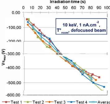
Fig. 8. Comparison of the temporal evolution of the surface potential of glass measured with the REPA method, during the four tests successively performed in the same irradiation conditions.
0 0
-100
-200>
-300 E -400 � -500 -600 -700 60 Irradiation time (s) 120 180 24020 keV, T
0 room•defocused beam
-200 pA - KP m ethod�200 pA- REPA method
�soo pA- REPA method
300
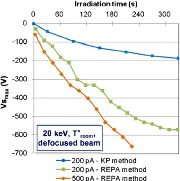
Fig. 9. Comparison of the temporal evolution of surface potential of borosiliG1te glass measured with the KP method (200 pAcm-2)and the REPA method (200 and
500 pA cm-2). -20 -70 � -120 -170 -220 Irradiation time (s) 0 60 120 180 240 300 360 420 480 540 600 Irradiation Relaxation
Fig. 10. Temporal evolution of surface potential of borosiliGlte glass during irradiation and relaX.1tion phases (KP method - 200 pA cm-2/20 keV/room tem
perature/defocused beam}
REPA method on irradiated dielectrics and to evaluate the mea surement reproducibility. Fig. 8 allows comparison between the irradiation phases of several tests successively performed in the same irradiation conditions. We notice that the charging kinetics are similar. lndeed, the Standard Deviation (SD) varies between 4% and 16%. Globally, the uncertainty approximately is Jess than -25 V. The relative uncertainty decreases when the surface poten tial increases. The uncertainty mainly depends on the voltage rise kinetics applied on the device grids by the operator. ln fact, the uncertainty will be greater if the applied grid voltage kinetics is high. Consequently, this measurement device is adapted to charac terise insulators because their surface potential is usually much greater than the instrumental uncertainty.
Fig. 9 demonstrates the REPA method consistency. We indeed notice (as expected) an increase of charging kinetics with the inci dent electron current. Moreover, ifwe compare the charging kinet ics measured with the KP and REPA methods under the same irradiation conditions, a significant difference between both mea surements is obseived. The charging kinetics is Jower with the KP method. This feature is due to the fact that potential relaxation occurs between irradiation shut down and surface potential mea surements with KP. A dead time (About 20 s for the round trip) is induced since KP measurements are performed without sample irradiation. The charges relaxation in this glass sample is sig nificant as shown after 450 s (beam off) in Fig. 1 O. At the beginning of the relaxation phase there is a decrease of about 30 V in 20 s. Such a decrease can also occur during each measurement dead time in irradiation phase. There is a voltage Joss accumulation up to equilibrium. Consequently, the surface potential of glass is underestimated during the irradiation time with the KP method, which is not obseived with the REPA method since no dead time is present in this second method.
4. Conclusion
ln this paper we have described the development and the opti misation of an instrumental device (REPA) that allows measuring the surface potential of dielectrics under continuous electron irra diation. The measurement method was validated through a calibration procedure on the prototype REPA An optimised REPA was designed and developed, thanks to numerical SPIS Simulations which allowed understanding the electrostatic con figuration of this operating device. The geometry of this small removable REPA device may be easily extended in other facility or application to evaluate the material charging in real time.
First results of characterisation have been obtained using this optimised device. The presented results allow demonstrating the acceptable measurement accuracy of this device. Moreover, these results emphasise the interest of measuring charging kinetics with a greater frequency on quite conductive dielectric material, which is more feasible with this REPA technique (in comparison with the KP method) without any electron beam switch off.
However, it will be interesting to characterise other materials in order to better evaluate the efficiency of this device. lt is also pos sible to optimise further this device by reducing its size and by changing the grids position in order to improve the measurement accuracy of the current signal.
Acknowledgements
Authors would like to thank M. Belhaj (ONERA, Toulouse) for his useful advices in this work as well as P. Sarrailh and J.C. Matéo Velez (ONERA, Toulouse) involved in the SPIS development who have contributed significantly to the software operation. We gratefully acknowledge the development team of SPIS and GMSH to let available in open source their software to the scientific corn munity. This Ph.D. work was supported by THALES.
References
(1 J R. Hanna, T. Paulmier, M. Belhaj, P. Molinie, B. Dirassen, O. Payan, N. Balcon, Characterization of charge Glrrier lateral conduction in irradiated dielectric materials,J. Phys. Appl. Phys. 44 (44) (2011) 445402.
(21 M. Bai, R.F.W. Pease, C. Tanasa, MA. McCord, O.S. Pickard, O. Meisburger, Charging and discharging of electron beam resist films. J. Vac. Sei. Technol. B 17 (6) (1999) 2893-2896.
(3 J J. Hodges, J. Hayes, J.R. Dennison, R. Hoffmann, Measurement of charging and discharging of high resistivity spacecraft materials by electron beams, in: 47th AJAA Aerospace Sciences Meeting including The New Horizons Forum and Aerospace Exposition, AmeriGln lnstitute of Aeronautics and Astronautics.
[4]H. Seiler, Secondary electron emission in the scanning electron microscope, J. Appl. Phys. 54 (11) (1983) R1–R18.
[5]L. Reimer, M. Riepenhausen, Detector strategy for secondary and backscattered electrons using multiple detector systems, Scanning 7 (5) (1985) 221–238. [6]M.M. El-Gomati, C.G.H. Walker, X. Zha, Towards quantitative scanning electron
microscopy: applications to nano-scale analysis, Nucl. Instr. Meth. Phys. Res. 645 (1) (2011) 68–73.
[7]T. Koshikawa, R. Shimizu, Secondary electron and backscattering measurements for polycrystalline copper with a spherical retarding-field analyser, J. Phys. Appl. Phys. 6 (11) (1973) 1369.
[8]E. Menzel, E. Kubalek, Secondary electron detection systems for quantitative voltage measurements, Scanning 5 (4) (1983) 151–171.
[9]O.C. Wells, C.G. Bremer, Improved energy analyser for the scanning electron microscope, J. Phys. E 2 (12) (1969) 1120.
[10]H.P. Feuerbaum, Electron beam testing: methods and applications, Scanning 5 (1) (1983) 14–24.
[11]E. Wolfgang, P. Fazekas, H.-P. Feuerbaum, R. Lindner, Electron-beam testing of VLSI circuits, IEEE J. Solid-State Circuits 14 (2) (1979) 471–481.
[12]Y. Goto, A. Ito, Y. Furukawa, T. Inagaki, Hemispherical retarding type energy analyser for IC testing by electron beam, J. Vac. Sci. Technol. 19 (4) (1981) 1030–1032.
[13]M. Ya-li, T. Fu-jun, X. Yu-xiong, C. Yi-feng, G. Xin, W. Yi, T. Kai, Y. Ze-dong, Retarding potential analyzer design and result analysis for ion energy distribution measurement of the thruster plume in the laboratory, World Acad. Sci. Eng. Technol. 71 (2012) 1890.
[14] LibreSource – SPIS documentation: <http://dev.spis.org/projects/spine/home/ spis/documentation>.
[15]T. Gineste, M. Belhaj, G. Teyssedre, N. Balcon, J. Puech, A novel experimental setup for the measurement electron backscattering yield, Meas. Sci. Technol. 25 (8) (2014) 085601.
[16]J. Roussel, G. Dufour, J.-C. Mateo-Velez, B. Thiebault, B. Andersson, D. Rodgers, A. Hilgers, D. Payan, SPIS multitimescale and multiphysics capabilities: development and application to GEO charging and flashover modeling, IEEE Trans. Plasma Sci. 40 (2) (2012) 183–191.
[17]J. Roussel, F. Rogier, G. Dufour, J.-C. Mateo-Velez, J. Forest, A. Hilgers, D. Rodgers, L. Girard, D. Payan, SPIS open-source code: methods, capabilities, achievements, and prospects, IEEE Trans. Plasma Sci. 36 (5) (2008) 2360–2368. [18]J.-F.R.C. Geuzaine, GMSH: a three-dimensional finite element mesh generator with built-in pre- and post-processing facilities, Int. J. Numer. Methods Eng. (2009) 1–24.