HAL Id: tel-01666039
https://tel.archives-ouvertes.fr/tel-01666039
Submitted on 18 Dec 2017HAL is a multi-disciplinary open access archive for the deposit and dissemination of sci-entific research documents, whether they are pub-lished or not. The documents may come from teaching and research institutions in France or abroad, or from public or private research centers.
L’archive ouverte pluridisciplinaire HAL, est destinée au dépôt et à la diffusion de documents scientifiques de niveau recherche, publiés ou non, émanant des établissements d’enseignement et de recherche français ou étrangers, des laboratoires publics ou privés.
Development of characterization methods for thin film
solar photovoltaics using time-resolved and
hyperspectral luminescence imaging
Gilbert El Hajje
To cite this version:
Gilbert El Hajje. Development of characterization methods for thin film solar photovoltaics using time-resolved and hyperspectral luminescence imaging. Materials Science [cond-mat.mtrl-sci]. Université Pierre et Marie Curie - Paris VI, 2016. English. �NNT : 2016PA066604�. �tel-01666039�
ÉCOLE DOCTORALE : ED 397 – Physique et Chimie des Matériaux
THÈSE
présentée par :Gilbert EL-HAJJE
Soutenue le : 16 Décembre 2016
Pour obtenir le grade de :
Docteur de l’université de Pierre et Marie Curie
Discipline/ Spécialité: Physique des Matériaux
Développement de nouvelles méthodes de caractérisation
optoélectroniques des cellules solaires photovoltaïques par
imagerie de luminescence
Devant le jury composé de:
Dr GUILLEMOLES Jean-François Directeur de thèse
Dr LOMBEZ Laurent Encadrant de thèse
Mr ORY Daniel Encadrant de thèse
Dr. KLEIDER Jean-Paul Rapporteur
Dr. BALOCCHI Andrea Rapporteur
Dr. ROCA i CABARROCAS Pere Examinateur
Dr. UNOLD Thomas Examinateur
Dr. FRAGOLA Alexandra Examinateur
Dr. PAUL Nicolas Examinateur
UNIVERSITÉ DE PIERRE ET
MARIE CURIE
2
ليحر ىركذ يف
ةموحرملا
،زور يتدج
ةموحرملا
،نيليه يتدج
موحرملا
جروج يدج
و
موحرملا
يدج
قيفوت
.
.عوسي اي ةيدبلأا ةحارلا يطعأ مهل
.نيمأ
4
Development of characterization methods for thin
film solar photovoltaics using time-resolved and
hyperspectral luminescence imaging
Gilbert El-Hajje
6
____________________________________________________________________________
ACKNOWLEDGMENTS
Après trois ans de thèse au sein de l’IRDEP, il est sans doute vrai qu’une thèse est une formation par la recherche et pour la recherche. On se lance dans des études doctorales très souvent poussé par notre ambition, par notre passion envers la recherche, et surtout, par notre volonté de vouloir réaliser des découvertes et être pionnier dans son domaine. A un certain point qui succède le point de démarrage de la thèse, on se rend compte rapidement, qu’avoir une bonne performance de chercheur scientifique n’est tout simplement pas suffisant. On s’aperçoit que très souvent, ce qui compte le plus, est l’aspect « humain » des choses, et le support moral qu’on a la chance de recevoir de la part de notre entourage. Ceux qui nous suivent et encadrent de plus près sont dans un premier plan les personnes de notre famille et les personnes appartenant à notre cercle de vie privée mais incontestablement aussi, les personnes qui se sont engagées à être encadrantes de notre travail doctoral. Ces-dernières, ce sont les personnes qui choisissent de superviser nos travaux, les diriger, faire en sorte à ce qu’on avance sur chaque aspect à la fois personnel et scientifique.
Dans mon cas, j’ai eu la chance d’avoir à mes côtés, tous les jours, deux encadrants exceptionnels : Laurent Lombez et Daniel Ory. Commençons par Dr. Lombez, AKA « Le Médecin des Cellules Solaires ». Il s’agit d’un personnage scientifique qui malgré son jeune âge, est déjà reconnu à l’international pour ses remarquables travaux de recherches sur le photovoltaïque. Je le remercie infiniment pour être toujours à l’écoute, toujours disponible. Son riche expérience fait de lui la personne vers laquelle je me dirige dans les situations les plus dures (i.e. les soumissions et les taches de dernière-minute, les problèmes techniques insurmontables et pleins d’autres « worst case scenario »). Ses conseils toujours pertinents et sa capacité à proposer des solutions innovantes ont été un moyen indispensable à ma réussite. Passons à la deuxième personne de mon « duo d’encadrants », AKA « Le Monsieur Ory ». Son expérience très riche et vaste dans le milieu professionnel avant de se lancer dans la R&D, a été aussi un premier atout pour solutionner la majorité de mes problèmes techniques (optomécaniques plus précisément). Je le remercie en premier lieu pour être une personne toujours à l’écoute de mes problèmes (parfois non intéressants), pour sa patience, son suivi régulier et surtout pour le temps qui m’a réservé. Je n’oublierai jamais nos fameuses séances de « brainstorming » très
7
fructueuses, génératrices de PI. En plus de sa passion pour la mécanique, je suis fier de lui faire découvrir une nouvelle passion, qui est aujourd’hui la sienne, « Le MaaMoul Libanais » !
Un pilier indispensable pour mes travaux de thèse, fut mon directeur de thèse, Dr. Jean-François Guillemoles. Je souhaite avant tout le remercier pour avoir accepté de diriger ma thèse. Je le remercie surtout pour ses interventions, ses commentaires, ses conseils et ses avis toujours aussi pertinents. Son rôle d’expert dans la recherche scientifique fut surtout essentiel en matière de progression et d’évolution. Il m’a appris certaines éthiques et moyens de communication dans le milieu scientifique qui est assez compétitif, rendant ma progression plus efficace et fluide. Je lui serai toujours reconnaissant.
Dans un cadre plus global, je tiens à exprimer ma gratitude envers l’ensemble du personnel de l’IRDEP. Une pensée particulière va à l’équipe remarquablement masculine du bâtiment F : Laurent, Daniel, Jean, Pierre, François, Trung, Enrique, et la liste est certainement non exhaustive. La « super » bonne ambiance créée par cette équipe m’a offert un environnement de travail exceptionnellement agréable. Je compte sur vous pour maintenir le niveau «assez particulier » des blagues et des histoires (les gens du F comprendront ;)) . Finalement, je tiens aussi à remercier toutes les personnes du bâtiment K, votre accueil a toujours été chaleureux et amicale. Un grand merci aussi aux différents doctorants pour les beaux moments passés ensemble à l’IRDEP ou même pendant les conférences : François, Sébastien, « Solénge », Charlène, Fabien, Julien et encore une fois la liste est non exhaustive !
Finalement, et pour bien conclure cette section, j’offre ces travaux de thèse à mes parents qui, grâce à eux, je suis à ce stade d’études et de réussite aujourd’hui. J’offre ces travaux aussi à mes frères Georges et Magid, ma famille entière, ma femme Salma, mes amis Rémie (Ramroum), Mario, Guy, Rami, Imad et beaucoup d’autres. Leur présence dans ma vie a été une source de réconfort et d’inspiration dans les moments les plus dures. Je vous remercie pour tout.
Mes sincères salutations
9
Contents
Index of Symbols ... 1
Introducing the PhD project ... 5
The General Context of Photovoltaic Energy ... 7
Chapter I. Theoretical background on CIGS PV devices and their luminescence properties ... 10
1.1 Chalcogenide Cu(In,Ga)Se2 thin-film technology ... 10
1.1.1 Introduction on CIGS PV technology & Cell configuration ... 11
1.1.1.1Back Contact ... 12
1.1.1.2CIGS Absorber Layer – Deposition Methods ... 12
1.1.1.3CdS Buffer Layers ... 13
1.1.1.4Front Contact ... 13
1.1.2 The particular case of micro-CIGS solar cells used in our experiments ... 16
1.2 Physics of PV device luminescence ... 17
1.2.1 Recombination Mechanisms ... 18
1.2.2 Time-Resolved Photoluminescence (TRPL) ... 23
1.2.3 Generated carrier dynamics under the influence of electric fields ... 25
1.2.4 Spectrally Resolved Photoluminescence ... 26
1.2.5 Spectrally-Resolved Electroluminescence & LED-PV Reciprocity Relations ... 28
1.2.6 Reciprocity between Photoluminescence and Electroluminescence of solar cells ... 31
1.2.7 Information derived from the luminescence intensity, its spectral and spatial variations ... 31
1.3 TRPL studies on CIGS solar cells: The literature contradiction dilemma ... 32
1.3.1 Theoretical aspect: Physics of charge carrier dynamics in Cu(In,Ga)Se2 PV devices ... 32
1.3.2 Photo-excitation-dependent TRPL decay analysis on CIGS ... 33
1.3.3 Voltage-bias-dependent TRPL decay analysis ... 35
1.3.4 Photo-excitation energy-dependent TRPL decay analysis ... 37
Chapter II. Optoelectronic Characterization of PV Devices ... 38
2.1 Standard Solar Cells Characterization Techniques ... 38
2.1.1 J-V Characteristics ... 38
2.1.2 External Quantum Efficiency ... 40
2.1.3 Capacitance-based Techniques ... 42
2.2 Advanced Luminescence-Based Characterization Techniques ... 43
2.2.1 Hyperspectral Imager ... 44
2.2.2 Scanning Confocal Microscope (SCM) ... 45
2.2.3 Comparison between the HI and the SCM ... 47
10
2.2.4.1Overview of technologies and Operating principles of TRFLIM ... 48
2.2.4.2Design and development of a setup dedicated to TRFLIM ... 50
2.2.4.3Spatial and Temporal resolutions of the detection system ... 52
2.2.4.4Characteristics of the excitation system ... 58
2.2.4.5Concluding the construction of the complete TRFLIM setup with a proof of concept ... 60
Chapter III. Quantitative local access to optoelectronic properties of Cu(In,Ga)Se2 PV devices using Time-Resolved Luminescence ... 62
3.1 General introduction and objectives ... 62
3.2 Development of a unified understanding of charge carrier dynamics in Cu(In,Ga)Se2 PV devices ... 62
3.2.1 Introduction ... 62
3.2.2 Physical model based on carrier recombination centers and shallow defects acting as carrier traps 63 3.2.3 Photo-excitation intensity-dependent and electrical carrier-injection dependent time-resolved luminescence experiments ... 65
3.2.4 Investigating the potential influence of the built-in electric field ... 69
3.2.5 Identifying the characteristics of probed carrier recombination ... 72
3.2.6 Brief summary and conclusion ... 76
3.3 Optical alternative for the study of metastabilities in Cu(In,Ga)Se2 PV devices ... 77
3.3.1 Metastabilities-induced distortions of Current-Voltage characteristics ... 77
3.3.2 Optical evidence of the effect of metastabilities activation on minority carrier dynamics ... 79
3.3.2.1Introduction & Methodology ... 79
3.3.2.2Basic Characterization ... 80
3.3.2.3Qualitative optical observation of a blue photon recovery effect ... 82
3.3.2.4Hysteresis cycle of the “DCD” parameter ... 84
3.3.2.5Hysteresis cycle of the carrier trapping lifetime ... 86
3.3.2.6Brief Conclusion ... 87
3.4 Contactless quantification of trapping defects density in Cu(In,Ga)Se2 PV devices ... 88
3.4.1 Development of a physical model for the reconstruction of the time-resolved luminescence decays88 3.4.2 Application to the photo-excitation intensity-dependent time-resolved luminescence decays ... 92
3.4.3 Application current injection-dependent time-resolved luminescence decays ... 93
3.4.4 Discussion on the application to the photo-excitation intensity-dependent and current injection-dependent time-resolved luminescence decays ... 94
3.4.5 The effect of the trapping defects density on global photovoltaic performance ... 94
3.4.6 An attempt at a quantitative optical spectroscopy of trapping defects ... 97
3.4.7 Discussing the choice, the limitations and relevance of the physical model ... 101
Chapter IV. Quantitative luminescence-based imaging of optoelectronic properties of thin filmPV devices102 4.1 Introduction... 102
4.2 Spatially-resolved, spectrally-resolved and time-resolved luminescence of Cu(In,Ga)Se2 PV devices ... 103
4.2.1 Quantitative electrical mapping of the variations of PV performance indicators following metastabilities activation ... 103
11
4.2.2 Quantitative optical mapping of trapping defects-induced variations in PV performance indicators107 4.2.2.1Mapping the effect of light-soaking on the quasi-Fermi levels splitting deduced from
electroluminescence imaging ... 107
4.2.2.2Micrometric mapping of charge carrier lifetimes and trapping activity ... 110
4.2.2.3Optical micrometric mapping of the absolute trapping defects density ... 114
4.2.2.4Mapping the micrometric losses in quasi-Fermi levels splitting ... 115
4.2.2.5Investigating the effect the photo-excitation energy ... 118
4.3 Time-Resolved Fluorescence Lifetime Imaging (TRFLIM) of Solar Cells ... 121
4.3.1 GaAs solar cell – An experimental study ... 121
4.3.2 GaAs solar cell – A numerical study & material properties extraction ... 126
Conclusion ... 131
Bibliography ... 134
List of peer-reviewed publications & proceedings ... 143
Appendix A ... 144
Résumé ... 147
1
Index of Symbols
Symbol Unit Description
𝑎 cm-1 Absorptivity
𝐴
% Absorption probability
AM1.5 Air Mass 1.5
𝐵𝑟𝑎𝑑 cm3s-1 Radiative recombination coefficient
𝑐 ms-1 Light velocity
𝐶 F Capacitance
𝐶𝑛, 𝐶𝑝 cm6s-1 Auger recombination coefficient for electron and hole
CBD Chemical bath deposition
DCD Dominant Carrier Dynamics parameter
𝐷𝑛, 𝐷𝑝 cm²s-1 Diffusion coefficient of electron and hole
𝐸 Vcm-1 eV Electric field Photon energy EL Electroluminescence a
E
eV Activation energy𝐸𝑐,, 𝐸𝑣, eV Conduction and valence band edge of semiconductor
𝐸𝑓 eV Fermi level
𝐸𝑓𝑛, 𝐸fp eV Quasi-Fermi level of electrons and holes
𝐸𝑔 eV Energy bandgap of semiconductor
n
e
s-1 Electron emission ratet
E
eV Trap energy level𝐸𝑄𝐸 % External quantum efficiency
𝑓 Occupancy of defect states
𝑓𝑐 % Collection function (probability to collect a photogenerated carrier)
𝐹𝐹 % Fill factor
FWHM Full Width at Half Maximum
𝐺 cm-3s-1 Generation rate
2
2 / , hh eV.s Planck’s constant, and Planck’s reduced constant
HI Hyperspectral Imager
𝐼 A Current
TRPL
I
Hits.s-1 Time-resolved photoluminescence decay intensityTRL
I
Hits.s-1 Time-resolved luminescence decay intensitytot TRPL
I
Hits.s-1 Integrated time-resolved photoluminescence decay intensityIQE % Internal Quantum Efficiency
𝐽 A.cm-² Current density
inj
J cm-2.s-1 Density of injected current flux 𝐽𝑠𝑐 A.cm-² Short-circuit current density
𝐽𝑝ℎ A.cm-² Photocurrent density 𝐽0 A.cm-² Saturation current density
rad o
J A.cm
-²
Radiative short-circuit current density
𝐽01 A.cm-² Saturation current density for the dark current of ideality A=1 𝐽02 A.cm-² Saturation current density for the dark current of ideality A=2
𝑘 Boltzmann constant
𝑁𝐴,𝑖, 𝑁𝐷,𝑖 cm-3 Acceptor and donor density in the semiconductor
N.A. Numerical Aperture
t
N
cm-3 Electron trap density1
N
cm-3 Carrier population occupying the valence band 2N
cm-3 Carrier population occupying the accessible density of trap states 3N
cm-3 Carrier population occupying the conduction bandPL Photoluminescence
PSF m Point Spread Function
𝑃𝑚𝑎𝑥 W Maximum power generated by a solar cell
𝑞 C Elementary charge
rad
R
s-1 Radiative recombination rate𝑅𝑠 ohm or ohm.cm² Series resistance 𝑅𝑠ℎ ohm or ohm.cm² Shunt resistance
SRH
R
s-1 Shockley-Read-Hall recombination rate𝑆𝑛, 𝑆𝑝 cm.s-1 Recombination velocity of electron and holes
SCM Scanning Confocal Microscope
3
SR A.W-1 Spectral Response
T K Temperature
TFRLIM Time-resolved fluorescence lifetime imaging
TRL Time-resolved luminescence TRPL Time-resolved photoluminescence V V Voltage 𝑉𝑜𝑐 V Open-circuit voltage rad oc
V V Radiative open-circuit voltage
𝑉𝑏𝑖 V Built-in voltage
𝑊 cm Width of the space charge region in the absorber
occ c
WRe Occurrence weight of direct carrier recombination events
occ Traps
W
Occurrence weight of carrier trapping eventsPL
Y
cm-2.sr-1.eV-1.s-1 Photoluminescence yield
cm-1 Absorption coefficient of the semiconductor∆𝜇 eV Quasi-Fermi levels splitting
eff
µ
eV Effective quasi-Fermi levels splitting
eV Central, statistical Quasi-Fermi levels splitting value
𝜀 Fm-1 Dielectric function
𝜎𝑛, 𝜎𝑝 cm2 Capture cross-section for electrons and holes 𝜈𝑛𝑡ℎ, 𝜈𝑝𝑡ℎ cm.s-1 Thermal velocity of electron and hole
𝜙 cm-2.sr-1.eV-1.s-1 Luminescence flux
𝜙𝑏𝑏 cm-2.sr-1.eV-1.s-1 Spectral photon density of a black body
𝜆 cm Wavelength
𝜂 % Solar cell efficiency
PL
% Photoluminescence efficiency𝜌 ohm.cm Resistivity
m Penetration depth
𝜓𝐷 cm-3 Density of trap states
𝜇𝑛, 𝜇𝑝 cm².V-1s-1 Electron and hole mobility in semiconductor
b
s Bulk minority carrier lifetimecap
s Carrier capture lifetimeem
s Carrier emission lifetime𝜏𝑛, 𝜏𝑝 s Carrier lifetime
rad
4
c
Re
s Recombination centers-related carrier lifetimetot
s Total carrier lifetimeTraps
s Carrier trapping lifetimev rec
5
Introducing the PhD project
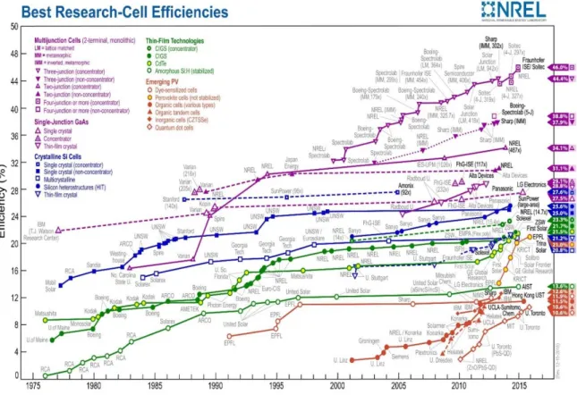
From the evolution of the solar power conversion efficiencies of photovoltaic solar cell technologies, we can learn that the second generation thin-film solar photovoltaics are progressively catching up with monocrystalline-based silicon solar cells. There is no doubt that the latter are occupying the vast majority of today’s market shares both in terms of production and installation. However, with CIGS-based thin film PV recently surpassing the record efficiency of multicrystalline silicon, it is safe to expect that second generation thin film PV could indeed start to occupy an increasingly important market share in the PV industry. Such increase in efficiency will eventually induce an increase in the production of the thin film PV panels. However, CIGS-based PV is known to suffer from instabilities issues due its material composition and metastabilities, even at the PV panel scale. Therefore, the future industries dedicated to its production, would be in need of special in-line characterization methods to closely monitor and examine this material that is much more complex than the typical monocrystalline silicon.
CIGS-based PV is at the heart of my PhD project. My aim is to develop new and innovative, luminescence-based characterization methods that have industrial applications. The reason, for which we chose the luminescence of PV devices as a tool, is because it can be optically generated and detected, without the need to physically contact the PV device, which is the case for photoluminescence. This contactless nature of this technique boosts is potential for industrial applications. Throughout my PhD I started by developing different methodologies and revisited the temporal aspect of the photoluminescence of CIGS solar cells. With these methodologies, I translated this aspect into key photovoltaic parameters and properties of the solar PV device. Then, by combining the spectral and temporal aspect of their luminescence, I developed a tool for a contactless evaluation of PV performance losses in the different areas of a thin film PV device. All of the developed methods were applied at both the local and global scale of the CIGS solar cell, using the scanning confocal microscope and the hyperspectral imager setups. Luminescence imaging the spatial aspect to all of my findings and helped us assess the spatial behavior of its PV performance and parameters.
The final part of my PhD was dedicated to the design, the development and the exploit of a new optical characterization setup at IRDEP. The latter is built to perform time-resolved fluorescence lifetime imaging. This technique has so far been used in the fields of biology, organic chemistry and in medicine. My goal was to build a setup that can be used for the characterization of the different PV
6
technologies. I will present the different building steps of the setup, the evaluations of its characteristics and finally present a panel of proofs of concept on PV devices, and some applications.
I would finally like to add that in addition to all of the above, I worked in parallel on a collaboration with a team from the University of Valencia. The aim of this collaboration was to quantify the spatial inhomogeneities of the properties of perovskite-based solar cells by mapping their luminescence. I summarize in Appendix A the main findings of this collaboration.
7
The General Context of Photovoltaic Energy
After decades of industrialized growth mainly sustained by fossil energies, tremendous quantities of greenhouse gases have been emitted in the atmosphere. Those gases, mainly methane and carbon dioxide accumulate in the atmosphere and contribute to the warming of our planet, thus confronting our society to the challenge of drastically reducing their emission. According to the International Panel on Climate Change (IPCC) Fourth Assessment Report [1], the carbon dioxide concentration has risen from 280 ppm in the pre-industrial era – late eighteenth century - to approximately 380 ppm nowadays. Keeping the rate of greenhouse gas emissions at its present level would eventually lead to a global carbon dioxide concentration of about 450 to 650 ppm by 2100. Depending on the considered energetic scenario, we would be lead to a mean global temperature increase of 1.1 to 6.4 degrees, thus causing drastic climatic changes [1]. We must thus act as soon as possible in order to reduce both our energy consumption and our dependence towards carbon-intensive solutions, among which fossil fuels. The sector of energy production contributes for about 25.9% to our carbon dioxide emissions. Within the energy sector, electricity production represents about 30% of these emissions. It is thus necessary to look for alternative ways of producing electricity. Solar energy is the most abundant form of energy on Earth. The incident energy that reaches our planet is about 2.1012 GWh over the course of a whole year, which is the equivalent of 11,000 times the yearly global energy consumption. We can see that there is an incomparable potential to be used, and the photovoltaic technology is one way to take advantage of this potential. Even in a country with a very average illumination level, such as France, the entire electricity demand can be met by covering 1% of the surface of the country with a system that has a conversion efficiency as low as 10%. Such a surface represents only one sixth of the constructed area in the country.
8
Figure 1: Annual average solar irradiance
Photovoltaic technologies remain the most commonly used solar energy collecting technologies today and will continue to see rapid and steady growth. Each of these photovoltaic technologies have its own advantage and drawbacks and it is not certain which one will dominate the market in the following decades; however it is certain is that the photovoltaic technologies will help countries develop a clean and renewable future.
Finally, Fig. 2 below illustrates the evolution throughout the years of the solar power conversion laboratory efficiencies of the major solar PV technologies:
9
10
Chapter I.
Theoretical background on CIGS PV devices
and their luminescence properties
Photovoltaics (PV) is a method of generating electrical power by a direct conversion of solar radiation into current electricity using semiconductors with an overall conversion efficiency that ranges from 20% to 35% depending on the considered technology. Photovoltaic solar panels are the most commonly used solar technology to generate electricity energy. They can act as small decentralized power stations when simply placed on the top of a roof. The electricity produced by household possessing photovoltaic panels is usually sold to the network at a higher price than the market price, thus allowing the investor to get his money back. In countries such as Germany or France, the existence of a feed-in tariff has largely contributed to the development and popularity of this technology [2]. Centralized production in photovoltaic farms is also a solution but can be problematic when competing with other uses of land. There are several kinds of solar PV technologies that are currently available. However, each of them is based on quite different concepts and science and each has its unique advantages. Analysis and comparison between different technologies can help adopt the most efficient and beneficial technology given a specific set of conditions.
1.1 Chalcogenide Cu(In,Ga)Se
2thin-film technology
Thin films are made by depositing thin layers of photosensitive materials in the micrometer (μm) range on a low-cost backing, such as glass, stainless steel or polymers. The first generation of thin film solar cell produced was a-Si. To reach higher efficiencies, thin amorphous and microcrystalline silicon cells have been combined with thin hybrid silicon cells. With II-VI semiconductor compounds, other thin film technologies have been developed, including cadmium telluride (CdTe) and copper-indium-gallium-diselenide(CIGS).The main advantages of thin films are their relatively low consumption of raw materials, high automation and production efficiency, ease of building integration and improved appearance, good performance at high ambient temperature, and reduced sensitivity to overheating. The current drawbacks are lower efficiency and the industry’s limited experience with lifetime performances. For utility production, thin film technologies will require more land than crystalline silicon technologies in order to reach the same capacity due to their lower efficiency. So, land availability and cost must be taken into consideration when thin film technology is considered. However, thin film technologies are growing rapidly. In recent years, thin film production units have increased from pilot scale to 50 MW lines, with some manufacturing units in the gigawatt (GW) range. As a result, thin films technologies are expected to increase their market share significantly by 2020.
11
Now several companies, such as Solar Frontier [5], TSMC-Solar [6], and MiaSolé [7], have begun operating facilities with over 100MW/yr production capacity.
1.1.1 Introduction on CIGS PV technology & Cell configuration
For some time, the chalcopyrite semiconductor CuInSe2 and its alloy with Ga and/or S [Cu(In,Ga)Se2 or Cu(In,Ga)(Se,S)2], commonly referred as CIGS, have been leading thin-film material candidates for incorporation in high-efficiency photovoltaic devices. CuInSe2-based solar cells have shown long-term stability and the highest conversion efficiencies among all thin-film solar cells, recently reaching 22.3% on a glass substrate [9]. A variety of methods have been developed to prepare CIGS thin film. Efficiency of solar cells depends upon the various deposition methods as they control optoelectronic properties of the layers and interfaces. CIGS thin film grown on glass or flexible (metal foil, polyimide) substrates require p-type absorber layers of optimum optoelectronic properties and n-type wide band gap partner layers to form the p-n junction. The current record for a CIGS solar cell grown on a flexible substrate is at 20.3% [10]. Transparent conducting oxide and specific metal layers are used for front and back contacts of CIGS solar cells.
Cell preparation starts with the deposition of back contact, usually Mo, on glass, followed by the p-type CIGS absorber, CdS or other weakly n-type buffer layer, undoped ZnO, n-type transparent conductor (usually doped ZnO: Al), metal grid, and antireflection coating. It requires an additional encapsulation layer and/or glass to protect the cell surface. The structure of a CIGS solar cell (seen in Figure 1.1 taken from ref [31]) is quite complex because it contains several compounds as stacked films that may react with each other. Fortunately, all detrimental interface reactions are either thermodynamically or kinetically inhibit at ambient temperature [12].
12
Figure 1.1: Schematic cross-section of a chalcopyrite-based thin-film solar cell.
1.1.1.1
Back Contact
Molybdenum (Mo) is the most common metal used as a back contact for CIGS solar cells. Several metals, Pt, Au, Ag, Cu, and Mo, have been investigated for using as an electrical contact of CIS- and CIGS-based solar cells [13– 15]. Mo emerged as the dominant choice for back contact due to its relative stability at the processing temperature, resistance to alloying with Cu and In, and its low contact resistance to CIGS. The typical value of resistivity of Mo is nearly 5 × 10⁻⁵ Ω cm or less. The preferred contact resistivity value is ≤0.3Ω cm. Results have been reported in several papers [13, 16, 17] concerning the influence of the mechanical and electrical properties of the Mo films on the performance of the photovoltaic devices. Molybdenum is typically deposited by e-gun evaporation [17, 18] or sputtering [19–21] on soda-lime glass which ideally provides an inexpensive, inert, and mechanical durable substrate at temperatures below 500–600◦C.
1.1.1.2
CIGS Absorber Layer – Deposition Methods
I–III–VI2 semiconductors, such as CIS or CIGS are often simply referred to as chalcopyrites because of their crystal structure. These materials are easily prepared in a wide range of compositions and the corresponding phase diagrams are well investigated [22–24]. For the preparation of solar cells, only slightly Cu-deficient compositions of p-type conductivity are suited [25, 26]. A wide variety of thin-film deposition methods has been used to deposit Cu(In,Ga)Se2 thin films. To determine the most promising
13
technique for the commercial manufacture of modules, the overriding criteria are that the deposition can be completed at low cost while maintaining high deposition or processing rate with high yield and reproducibility. Compositional uniformity over large areas is critical for high yield. Device considerations dictate that the Cu(In,Ga)Se2 layer should be at least 1 µm thick and that the relative compositions of the constituents are kept within the bounds determined by the phase diagram. The most promising deposition methods for the commercial manufacture of modules can be divided into two general approaches that have both been used to demonstrate high device efficiencies and in pilot scale manufacturing. The first approach is vacuum coevaporation in which all the constituents, Cu, In, Ga, and Se, can be simultaneously delivered to a substrate heated at 400◦C to 600◦C and the Cu(In,Ga)Se2 film is formed in a single growth process. The second approach is a two-step process that separates the delivery of the metals from the reaction to form device-quality films. Typically the Cu, Ga, and In are deposited using low-cost and low-temperature methods that facilitate uniform composition. Then, the films are annealed in a Se atmosphere, also at 400◦C to 600◦C. The reaction and anneal step often takes longer time than formation of films by coevaporation due to diffusion kinetics, but is compatible with batch processing.
1.1.1.3
CdS Buffer Layers
Semiconductor compounds with n-type conductivity and band gaps between 2.0 and 3.6 eV have been applied as buffer for CIGS solar cells. However, CdS remains the most widely investigated buffer layer, as it has continuously yielded high-efficiency cells. CdS for high-efficiency CIGS cells is generally grown by a chemical bath deposition (CBD), which is a low-cost, large-area process. However, incompatibility with in-line vacuum-based production methods is a matter of concern. Physical vapor deposition- (PVD-) grown CdS layers yield lower efficiency cells, as thin layers grown by PVD do not show uniform coverage of CIGS and are ineffective in chemically engineering the interface properties. The role of the CdS buffer layer is twofold: it affects both the electrical properties of the junction and protects the junction against chemical reactions and mechanical damage. From the electric point of view the CdS layer builds a sufficiently wide depletion layer that minimizes tunneling and establishes a higher contact potential that allows higher open circuit voltage value [27, 28]. The buffer layer also plays a very important role as a “mechanical buffer” because it protects the junction electrically and mechanically against the damage that may otherwise be caused by the oxide deposition (especially by sputtering).Moreover, in large-area devices the electric quality of the CIGS film is not necessarily the same over the entire area, and recombination may be enhanced at grain boundaries or by local shunts. Together with the undoped ZnO layer, CdS enables self-limitation of electric losses by preventing defective parts of the CIGS film from dominating the open circuit voltage of the entire device[29].
14
There are two main requirements for the electric front contact of a CIGS solar cell device: sufficient transparency in order to let enough light through to the underlying parts of the device, and sufficient conductivity to be able to transport the photo-generated current to the external circuit without too much resistance losses. Transparent conducting metal oxides (TCO) are used almost exclusively as the top contacts. Narrow lined metal grids (Ni–Al) are usually deposited on top of the TCO in order to reduce the series resistance. The quality of the front contact is thus a function of the sheet resistance, absorption and reflection of the TCO as well as the spacing of the metal grids [30]. Nowadays CIGS solar cells employ either tin doped In2O3 or, more frequently, RF-sputtered Al-doped ZnO.
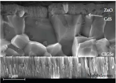
Once the full Cu(In,Ga)Se2 solar PV device deposition is made, the obtained result regarding the total stack is illustrated in Figure 1.2 taken from ref [11].
Figure 1.2: Scanning electron micrograph of the cross-section of a typical chalcopyrite solar cell with Cu(In,Ga)Se2 (CIGSe) absorber
15
Figure 1.3: Energy band diagram of a full CIGS PV device
It is well known that CIGS has a large deviation from stoechiometry attributed to antisite defects, vacancies and defect clusters in the material. Zhang [37] has calculated the transition energy for a large number of defects in CIS, and the results are summarized in Figure 1.4. Knowledge of the defect energies as well as their densities is an important input to develop meaningful device models. DLTS is a standard diagnostic technique for determining the trap properties such as trap energy level, capture cross section, and trap concentration.
16
1.1.2 The particular case of micro-CIGS solar cells used in our experiments
In usual studies on the inhomogeneities of the CIGS cells at the micrometer scale, standard laboratory samples are investigated. Compared to the area effectively probed, these cells are much larger (usually more than 0.1 cm2). Such areas may cause measurement artifacts. More precisely, when performing optoelectrical measurements one can suffer from sheet resistance effects under a high excitation flux when doing photoluminescence measurements. Thus, we will study in this thesis circular CIGS microcells, as presented in Figure 1.5. To underline the advantages of such a device, we introduce the general concept of the microcell.
The microcells are designed for use under concentrated sunlight. The main purpose of their development is to save material. Moreover, taking advantage of the light concentration, these cells demonstrated a 4% absolute efficiency increase when compared to corresponding large area cells [106, 107]. This increase results from the simultaneous logarithmic increase of the open-circuit voltage. Different aspects usually limit the concentrated photovoltaic technology (CPV). Firstly, strong current densities are reached (several A/cm2), resulting in resistive limitation of the front layer. Secondly the temperature may increase to result in a global efficiency loss. Due to their small scale, the microcells efficiently overcome these difficulties [107].
To elaborate on these cells, different fabrication techniques are explored. As a proof of concept, they were originally made of usual large cells that were artificially reduced. Their elaboration was made by Myriam Paire during her thesis at IRDEP [152].
This kind of cell is under study in this thesis. Previous characterization work on this type of solar cells has been done by Amaury Delamarre [153] during his PhD work. In particular, he performed hyperspectral luminescence imaging experiments on these devices to extract their properties such as the local dark saturation currents, the EQE, the quasi-Fermi levels splitting, the sheet resistance and current transport efficiency.
Our investigated samples are glass/Mo/CIGS/CdS/ZnO circular microcells with diameters varying between 20 µm and 30 µm. The 2µm thick CIGS absorber prepared using a three-stage co-evaporation method, possesses an optical bandgap energy Eg=1.1730 eV and the following composition ratios:
26 . 0 In Ga Ga & 78 . 0 In Ga Cu .
It is also to be noted that the CIGS absorber possess a V-shaped [Ga/ (Ga+In)] composition gradient. The CdS layer is deposited by Chemical Bath Deposition (CBD) technique. The bath is composed of cadmium acetate (Cd(CH3CO2)2), thiourea (SC(NH2)2) and ammonia (NH3) in aqueous solution. The deposition is done at 65°C under constant agitation during approximately 5 minutes. The samples are then rinsed in distilled water and any parasitic particle is removed by ultrasound. The thickness of the CdS layer is around 50 nm.
Finally the TCO layers were deposited by sputtering and consist of a 50 nm layer of i-ZnO and a 350 nm layer of ZnO-Al.
17
Figure 1.5: (a) SEM image and (b) scheme of a microcell structure. Figure from ref [106]
To obtain microcells, a 400 nm thick insulating SiO2 layer as well as a 20 nm/300 nm Ti/Au bilayer are deposited above the CdS layer. Holes obtained by photolithography in the SiO2 delimit the microcell. The ZnO layers are obtained by sputtering. The contact is therefore done at the perimeter of the cell by the Au layer. An SEM image of the resulting structure is shown in Fig.1.5(a). From a characterization point of view, such a structure is convenient as small areas are easily investigated by various setups. Moreover, we do not suffer from the top layer sheet resistance, so that electric measurement at the perimeter of the cell is directly comparable to the luminescence measurement. Such observations are usually made impossible by the large area cells. The CIGS luminescence being usually weak, strong excitation are needed (such as 10000 suns equivalent illumination), so that the efficient temperature management is also an advantage.
1.2 Physics of PV device luminescence
Luminescence is "cold light", light from other sources of energy, which can take place at normal and lower temperatures.
In the process of luminescence, when radiation is incident on a material some of its energy is absorbed and re-emitted as a light of a longer wavelength (Stokes law). In the process of luminescence, wavelength of light emitted is a characteristic of a luminescent substance and not of the incident radiation. The emission of light takes place at characteristics time after absorption of the radiation. The luminescence emission is seen to be spontaneous, thus it is seen to be taking place simultaneously with absorption of radiation.
The light emitted could be visible light, ultra-violet, or infrared light.
This cold emission, i.e. luminescence, involves two steps: (1) The excitation of electronic system of a solid material to higher energy state, and (2) subsequent emission of photons.
18
In the case of an external voltage applied as the excitation source, we speak of electroluminescence (EL), and in case, an incident light source is used, we speak of the photoluminescence (PL). Solar photovoltaic cells for example can reciprocally function as LEDs or current generators.
Therefore, the source of PL and EL radiation is the transition of electrons from higher occupied electronic states into lower unoccupied states where it recombines with a hole, under the emission of a photon. Comparing to other investigation techniques, PL methods offer several advantages in the field of PV, it is non-destructive, non-invasive, and can actually be performed at each fabrication step of our solar cells. We must note that there are other types of luminescence such as: Cathodoluminescence, thermoluminescence, etc…
In the first part of the chapter, we will be describing the classical mechanisms behind the physics of the luminescence of PV devices. That includes the radiative recombination process that matters the most of which is unavoidable.
In the second part, we will discuss the temporal aspect of photoluminescence and explaining the charge carrier dynamics and what one can expect to observe and deduce while performing time-resolved photoluminescence experiments.
In the third part, we switch from the description of the temporal to the spectral characteristics of the photoluminescence. In particular, we will be including the absorptivity of solar PV devices and end up by presenting and explaining the Generalized Planck’s law for luminescence emission that relates the intensity of the latter to the optical properties of the PV device.
In the final part of this chapter we will focus on the reciprocity relations between the functioning of a system in LED & and PV mode. This will include the description of the spectral characteristics of solar PV electroluminescence.
1.2.1 Recombination Mechanisms
In a nondegenerate semiconductor, the equilibrium density of electron-hole pairs is constant at a given temperature. The law of mass action [67] arises from thermodynamics and relates the product of electrons and holes to the intrinsic density, which is specific to a material. The law of mass action is written as:
)
(
2 0 0T
n
p
n
i (1.1)Here n0 is the free-electron density, p0 is the free-hole density at equilibrium, and ni (T) is the intrinsic
density at the absolute temperature T in degrees Kelvin. ni is related to the effective conduction-band Nc and valence-band Nv densities of states by the relationship:
19
E
kT
N
N
T
n
i2(
)
c vexp
g/
(1.2)Excess carriers can be electrically or optically injected into the semiconductor, creating a nonequilibrium concentration:
)
(
2T
n
np
i (1.3)Assuming that each quasi-Fermi level EFn & EFp is flat from the injecting contact through the majority carrier regions and throughout the space-charge region or SCR, only in the minority carrier regions, the quasi Fermi levels shall be allowed to vary. In the complete SCR the splitting of the quasi-Fermi levels equals the applied voltage bias and it holds:
kT qV n kT E E n np i2exp Fn Fp i2exp (1.4)
If one aims at deriving a general routine for the determination of the diode quality factors for different recombination mechanisms, equation (1.4) can be generalized as:
AkT qV n np i A A exp / 2 / 1, with A the diode quality factor. (1.5)
In equation (1.5), we distinguish between three different cases of carrier recombination mechanisms that will be detailed later on:
If A=1, then the regime corresponds to radiative electron-hole pair recombination. If A=2, then an electron or a hole is involved in a defect-related recombination. Finally, if A=3, three particles are involved in an Auger-type recombination mechanism.
Thermodynamics drives the system toward the equilibrium described by Eq. (1.2). In the absence of further injection, equilibrium is restored via various recombination mechanisms that will be discussed in this chapter. In an intrinsic material or under high-injection conditions, n ~p, and the recombination process is called bimolecular decay. Bimolecular recombination rates will be derived in this section. If the medium is extrinsically doped with donors or acceptors, the minority-carriers are holes or electrons, respectively. For the case of CIGS, a p-doped material forms the absorber of the PV device and the minority carriers are therefore electrons. We have:
A
N
p
0
, A i N n n 2 0 => p-doped CIGS (1.6)20
Here, p0 is the free hole-density that is derived from the law of mass motion. If both donors and acceptors are present, compensation occurs and:
A D
N
N
p
0
(1.7)Now, let’s assume that at t =0 the system is brought out of equilibrium , Δn, Δp excess electron, hole pairs per unit volume are produced by an injection pulse where:
0 0 ) , ( ) , ( ) , ( ) , ( p t x p t x p n t x n t x n (1.8)
Here n(x,t) and p(x,t) are the non-equilibrium electron and hole concentrations, respectively. It is to be noted that n0 and p0 can be position-dependent at the vicinity of the interfaces.
The solution for Δn(x, t) is found by solving the time-dependent continuity equation [68]. For field-free or quasi-neutral regions of the semiconductor, the continuity equation reduces to the time-dependent diffusion equation. The diffusion equation is a partial differential equation relating the net diffusion of minority carriers into a volume and the net recombination of the carriers within the volume. After the generation of electron-hole pairs, the diffusion equation for Δn(r, t) is given by:
)
,
(
)
,
(
)
,
(
n
r
t
t
r
n
D
t
t
r
n
(1.9)Here, τ is the recombination lifetime, which may also be a function of other parameters including Δn. Also, D is the minority electron diffusivity. For a general solution of this equation, one first assumes that the time and spatial variables can be separated. The electron concentration (Δn) can be written as:
)
(
)
(
)
,
(
r
t
f
t
g
r
n
(1.10)Substituting Eq. (1.10) into the diffusion Eq. (1.9), it can be shown that:
C
r
g
r
g
D
dt
t
df
t
f
)
(
)
(
1
)
(
)
(
1
2
(1.11)The left-hand side of Eq. (1.11) is a function of time only, and the right-hand side is a function of spatial variables only. Thus, each side of the equation must equal a constant that is designated by the value C. One can write an ordinary differential equation as a function of time for the left-hand side. Here, we will examine solutions of the time-dependent components of Δn(t) assuming that C = 0:
n
dt
n
d
(1.12)21
Equation (1.12) forms the basis for all of the upcoming theoretical and experimental sections. Such equation is extremely important. Based on it, we have a fist proof of the mathematical nature of the temporal evolution of the excess minority carrier density following a pulsed excitation. We can directly see that the time-decay of this density follows an exponential mathematical law. The decay time is called the minority carrier recombination lifetime “τ”.
In terms of minority carrier dynamics, the emitted luminescence intensity originates from radiative recombination between the generated electron-hole pairs. At this stage, we assign to these carriers a first definition of radiative recombination lifetime
rad. The intensity of the time-resolved luminescencesignal strictly depends on the rate at which occur these radiative events. This rate is called the radiative recombination rate
R
rad and depends on the excitation level. As Δnincreases so does the number ofradiative events and consequently the TRPL decay intensity increases. The rate can hence be expressed as: rad rad
n
dt
n
d
R
(1.13)For a p-doped and direct bandgap semiconductor such as a CIGS PV device, the radiative recombination coefficient is written as:
rad rad
p
B
01
(1.14)This will provide an expression for
R
rad as a function ofB
rad:n
p
B
R
rad
rad 0
(1.15)In high injection level scenario, to the bimolecular type of radiative recombinations, an Auger recombination is added, with Cp,n the Auger recombination coefficient. The recombination stops being
only bimolecular but becomes a mix of bi-molecular and three-carrier type of recombinations.
Similar to radiative recombination, Auger recombination also is an intrinsic recombination process which cannot be avoided and which is active in chalcogenide devices. The net recombination rate for Auger recombination is given by:
)
(
)
(
0 2 0 2 0 2 0 2p
n
p
n
C
n
p
n
p
C
R
Auger
p
n
(1.16)22
For a p-type absorber (such as a CIGS absorber) with
p
p
0
N
Awhich is exposed to small carrierinjection or medium excitation, the Auger excitation probability of an electron is very small due to the small number of electrons being minority carriers. Then, the Auger-limited lifetime is determined by hole excitation and it is expressed as:
n
N
C
R
Auger
p A2
(1.17)In a real PV device we find undesirable densities of localized states that originate from either impurities or mechanical defects such as dislocations. In addition, major sites of minority-carrier recombination are surfaces or interfaces that contain bonding defects. The energy levels of surface defects often lie in the forbidden gap, producing surface or interface states. The physics of the recombination at deep level defects is discussed later on.
We can hence deduce that other types of routes exist for carrier recombination in a semiconductor. The nature of these additional routes will strictly depend on the nature of these localized states and their characteristics such as their energy level within the forbidden gap, their chemical nature, their charge, capture cross section and many others.
The non-radiative recombination of electron-hole pairs at defect levels in the bandgap was first discussed by Shockley and Read [69] and by Hall [70]. Later work by Sah et al. [71] added to the understanding of the role of such defects. This common mechanism in minority-carrier kinetics is frequently called the Shockley-Read-Hall (SRH) recombination mechanism. The physics involves minority-carrier capture at defects that have quantum levels in the bandgap of the semiconductor. The SRH recombination rate is derived in most semiconductor textbooks [68, 72] and is shown to be:
kT
E
E
n
p
kT
E
E
n
n
n
pn
N
R
t i i p i t i n i t th n p SRHexp
exp
2
(1.18)and has units of cm-3s-1. Here, N
t is the volume density of deep levels;
pand
nare the hole andelectron capture cross-sections, respectively; and Et, is the energy level of the trap. The electron and hole concentrations are n and p, respectively, and
th is the thermal velocity that is considered identicalfor the electrons and holes. A logarithmic plot of RSRH versus Et – Ei shows a plateau at Et = Ei. The maximum non-radiative recombination rate occurs at defects levels that lie at or near midgap. When the defect energy level is near either band, thermal emission to the band quenches the recombination
process. For the case, when Et lies near Ec the denominator term
kT E E n t i
23
This term describes the emission of trapped electrons to the conduction band. Because of electron emission, the electron occupancy is small and the recombination rate is decreased.
1.2.2 Time-Resolved Photoluminescence (TRPL)
Based on all what we have discussed so far, we learned that three different routes can be taken by carriers after generation: Radiative bimolecular recombination, Auger recombination , non-radiative deep SRH recombination and carrier trapping by shallow electron or hole trap levels lying at the vicinity of the conduction and valence band. In figure 1.6 below we show a schematic illustration of these events:
Figure 1.6: Schematic diagram of impurity-related energy levels within the forbidden gap of a semiconductor. Levels are labeled as to whether the defect is likely to be a trap or a recombination center according to the
Shockley-Read-Hall model. (taken from Ref [65])
Figure 1.6 shows the forbidden gap of a semiconductor that has several types of impurity levels. Those near the midgap position are labeled recombination centers. Also shown are levels that are designated as electron traps and hole traps. These lie near the conduction band and the valence band, respectively. The defect level described by Eq. (1.18) may be either a trap or a recombination center, depending on Et. The defect level is a trap when the absolute value |Ei – Et| is large (~Eg/2) and the energy level Et, lies near either band. A captured hole or electron is thermally emitted back to the valence band or to the conduction band, respectively. In either type of trap, an emission term in the denominator of Eq. (1.18) dominates, and RSRH decreases many orders of magnitude relative to Et, being midgap. The demarcation between trapping and recombination centers is described in detail elsewhere [73]. If the energy level Et, lies near midgap Ei , RSRH becomes very large, and recombination is the most probable event. Thus, midgap centers (Et – Ei) are very effective recombination sites.
24
When more than one defect type is present, the total, low-injection lifetime is described by a single minority-carrier lifetime τ, where:
i i rad
1
1
1
(1.19)Here, τi is the non-radiative/trapping lifetime for each specific type of defect. Equation (1.19) results from the notion that recombination probabilities are additives. The defects here are assumed to be uniformly distributed in the volume of the semiconductor. They may be localized at specific locations in the material. In particular, recombination levels are usually generated at surfaces and interfaces because of the high concentration of impurities and bonding defects. These defects are the origin of the parameter called the surface or interface recombination velocity. In addition, under this low-injection condition, the Auger recombination rate is negligible.
From an experimental point of view, we remind that the TRPL signal is the result of the different recombination or trapping events. By decay dynamics we refer to its mathematical behavior. We have seen from the previous equations that it naturally obeys an exponential decaying law, only if τ is constant. However, does the presence of multiple types of lifetimes involve different decaying velocities? In other terms, can the TRPL decay present a mono, double or even triple exponential decay? Experimentally, as SRH events become more frequent, a weaker TRPL intensity is obtained. Unfortunately, this means that SRH events do not influence the dynamics of the decay but only its intensity and hence cannot be directly extracted. One can therefore conclude that two different samples with the same PV material under the same excitation conditions, can be compared based on the overall TRPL intensity. Such comparison can eventually provide relative information on their relative density of SRH states and their material quality.
For trapping events however, things become more interesting. Trapping does not lead to a loss of carriers but rather a delay factor of the radiative recombinations. Such characteristic is expected to have its direct signature on the TRPL decay as one could expect to observe two different decay lifetimes characterized by two states of carrier dynamics. The first state being related to direct radiative recombination events, and the second related to carrier trapping events. From a kinetics point of view, the delaying effect of traps would then be translated in a slower decay of the luminescence signal. Based on the previously combined knowledge of carrier dynamics, the temporal evolution of the luminescence intensity ITRPL(t) can be mathematically expressed as:
)
(
)
(
)
(
t
B
p
0n
t
C
p
02n
t
I
TRPL
rad
p
(1.20)25
Firstly, Equation (1.20) tells us that the luminescence intensity depends on the initial doping level of the CIGS solar cell and the excitation level of the PV device. For a given CIGS device, p0 is defined during
the device fabrication process. Δn however, can be varied experimentally by tuning the excitation level. Three cases can be defined: Case of low-moderate injection level according to which Δn0<<p0 , the case of moderate injection level for which Δn≥ p0 and the case of high injection level for which for which Δn>> p0. In the low and moderate injection level scenario, it is the bimolecular type of recombination that predominates. According to the literature [131], chalcogenide thin films exhibit radiative lifetime values
radin the range of 10-6 s.Up to a certain extent, at very high injection levels, it is possible that recombinations become purely Auger-type of recombination. Very few or no pure experimental data exist for the Auger coefficients of chalcogenide materials. In order to estimate the relative importance of Auger recombination for chalcogenide absorbers in thin film solar cells, we follow the argument of Bube [157] who gives a lower limit for the Auger coefficient of
C
p
10
28cm
6s
1.In addition, the lifetime of minority carriers in the Auger limit is given by:
Aug
(
C
pN
A2)
1. We learn from this expression, that the Auger recombination is the limiting process in the case of high doping concentrations. Hence, based on the Bube approximation for Cp, the Auger limited lifetimes for the doping densities of3 18 17 16 15
10
,
10
,
10
,
10
cm
N
A are
Aug
10
2,
10
4,
10
6,
10
8s
, respectively. We conclude that the Auger limited recombination would become critical for doping densities in the order of 1018cm3. In the upcoming experimental sections of the thesis we will present a methodology that leads to accurate extraction of lifetime and material information from a TRPL decay.1.2.3 Generated carrier dynamics under the influence of electric fields
In this section we will study one additional parameter that is believed to have an influence on the generated charge carriers. That parameter is the electric field that is created once the junction is formed within the photovoltaic material. We will also precise under which experimental conditions it is relevant to consider the effect of charge separation on the probed carrier dynamics.
R.K. Ahrenkiel[74] and A.J. Nozik [75] conducted through simulation work, the first rigorous studies of the effects of electric fields on the time-resolved photoluminescence spectra in III-V semiconductors. The need for this analysis originated from the fact that under experimental conditions where drift is important enough to have a clear influence on the recombination channels of charge carriers. The importance of the drift depends on the width of the space-charge region WSCR and the intensity of the
electric field. The experimental conditions such as the value of the applied voltage-bias and the photo-excitation level will determine the “screening” degree of the electric field.


![Applications de la Chimie Radicalaire des Xanthates : Synthèse d'Alcaloïdes d'Origine Marine ; Synthèse de Thiéno[2,3-b]thiopyranones ; Synthèse de Thioéthers Aryliques ; Approche à la Synthèse Totale du (+)-Maritimol.](data:image/gif;base64,R0lGODlhAQABAIAAAP///wAAACH5BAEAAAAALAAAAAABAAEAAAICRAEAOw==)