Millimeter-wave Antenna Selection Switch using Advanced
CMOS Technologies
by
Hoai Tan PHAM
THESIS PRESENTED TO ÉCOLE DE TECHNOLOGIE SUPÉRIEURE
IN PARTIAL FULFILLMENT FOR A MASTER’S DEGREE
WITH THESIS IN ELECTRICAL ENGINEERING
M.A.Sc.
MONTREAL, JULY 16, 2020
ÉCOLE DE TECHNOLOGIE SUPÉRIEURE UNIVERSITÉ DU QUÉBEC
© Copyright reserved
It is forbidden to reproduce, save or share the content of this document either in whole or in parts. The reader who wishes to print or save this document on any media must first get the permission of the author.
BOARD OF EXAMINERS (THESIS M.SC.A.)
THIS THESIS HAS BEEN EVALUATED BY THE FOLLOWING BOARD OF EXAMINERS
Mr. Nicolas Constantin, Thesis Supervisor
Department of Electrical Engineering, École de Technologie supérieure
Mr. Ambrish Chandra, President of the Board of Examiners
Department of Electrical Engineering, École de Technologie supérieure
Mr. Dominic Deslandes, Member of the jury
Department of Electrical Engineering, École de Technologie supérieure
THIS THESIS WAS PRESENTED AND DEFENDED
IN THE PRESENCE OF A BOARD OF EXAMINERS AND PUBLIC JUNE 26, 2020
ACKNOWLEDGMENT
I would like to express my sincere thanks to Professor Nicolas Constantin, who gave me the opportunity to study in Canada. Thank you for your dedicated instructions and your enthusiastic support that helped me to have more motivation to complete my thesis.
I also want to take this opportunity to thank my labmates at LACIME for all their support and discussions. Especially, I would like to thank Smarjeet for all the good things you taught me from the first day of my study.
I would also like to thank Sanjeev for his help during my time at Skyworks Solutions, Inc. Ottawa.
Mom, Dad! I am always thankful to you for your unconditional love and support.
Finally, I appreciate Skyworks Solutions, Inc. for giving me the opportunity to conduct research and collaborate through the Natural Sciences and Engineering Research Council of Canada (NSERC) Collaborative Research and Development (CRD) Grant.
Millimeter-wave antenna selection switch using advanced cmos technologies
Hoai Tan PHAM
RÉSUMÉ
L'objectif principal de ce travail de recherche est de développer un circuit de commutation d'antenne innovant sur circuit intégré (CI) CMOS pour les équipements de communication mobile de cinquième génération (5G).
Les objectifs spécifiques sont d'étudier, de concevoir, de simuler, de tester et de valider le fonctionnement du circuit de commutation d'antenne CMOS proposé fonctionnant à 28 GHz. Le circuit de commutation comprend un circuit de commutation SPDT (Single Pole Double Throw) sur une seule puce en technologie CMOS, ainsi que les lignes de transmission nécessaires intégrées dans un stratifié multicouche pour la connexion entre le circuit de commutation sur puce et les deux antennes.
La nécessité de la coexistence des technologies RF et ondes millimétriques (par exemple, les émetteurs-récepteurs WLAN dans la bande 5 GHz et les émetteurs-récepteurs de communication machine à machine dans la bande 28 GHz) dans les futurs équipements de communication sans fil impose des défis de conception et d'intégration dans le module Amplificateur de puissance (PA) destiné aux émetteurs frontaux.
Un aspect clé est la nécessité d'inclure des fonctions de commutation d'antenne à ondes millimétriques dans le même module PA tout en favorisant la miniaturisation. Cela nécessite une innovation dans la conception et l'intégration de circuits de commutation CMOS à faible perte sur le même CI PA 28 GHz. Cela complique également la conception de la partie frontale de l'émetteur, car elle nécessite des connexions à faible perte à partir du circuit intégré de l'amplificateur de puissance vers différents emplacements d'antenne RF et à ondes millimétriques sur le circuit imprimé (PCB) de l'équipement de communication.
Le point de départ est l'étude de la documentation de conception sur une structure de base d'un commutateur d'antenne à ondes millimétriques conçu chez Skyworks Solutions, Inc. Une étude approfondie accompagne cette recherche, à travers des simulations d'architectures et de circuits de commutation de pointe, une revue des techniques proposées dans la littérature ainsi que dans d’autres modèles industriels compatibles. Cette étude est suivie par la caractérisation des dispositifs CMOS, conjointement avec la conception des circuits de commutation requis. En particulier, des performances de commutateur clés, telles que l'obtention de pertes d'insertion plus faibles et une bonne isolation, avec une technologie CMOS avancée sont investiguées et démontrées par la conception d'un commutateur SPDT asymétrique. La perte d'insertion et l'isolement mesurés à 28 GHz de Tx à Rx sont respectivement de 0,9 dB et 28 dB.
Mots-clés: CMOS, commutateur unipolaire à double course (SPDT), ondes millimétriques,
semi-conducteur sur isolant (SOI), perte d’insertion, isolation, émetteur, récepteur. amplificateur.
Millimeter-wave antenna selection switch using advanced cmos technologies
Hoai Tan PHAM
ABSTRACT
The main objective of this research work is to develop an innovative on-chip CMOS-based antenna switching circuit for fifth-generation (5G) mobile communication equipment.
The specific objectives are to study, design, simulate, test, and validate the operation of the proposed CMOS-based antenna switching circuit operating at 28GHz. The switching circuit comprises an SPDT (Single Pole Double Throw) switch circuit on a single chip in CMOS technology, along with the necessary transmission lines embedded into a multi-layer laminate for the connection between the on-chip switch circuitry and the two antennas.
The necessity for the coexistence of RF & mm-wave technologies (e.g., WLAN transceivers in 5GHz band and machine-to-machine communication transceivers in the 28GHz band) in future wireless communication equipment imposes integration design challenges in the Power Amplifier (PA) module intended for the transmitter front-ends. A key aspect is the necessity to include mm-wave antenna switching capabilities in the same PA module while favoring miniaturization. This requires innovation in the design and integration of low-loss CMOS switching circuits on the same 28 GHz PA IC. It also complicates the design of the transmitter front-end, as it requires low-loss transmission paths from the Power Amplifier IC to different RF & millimeter-wave antenna locations on the communication equipment’s PCB.
The starting point is the study of the design documentation on a basic structure of a millimeter-wave antenna switch designed at Skyworks Solutions, Inc. An in-depth investigation accompanies this study through simulation of state-of-the-art switch architectures and circuit techniques proposed in the literature as well as other compatible industrial designs. This study is followed by the characterization of CMOS devices in conjunction with the design of switch circuitry. In particular, key switch performance metrics such as achieving lower insertion losses and good isolation with advanced CMOS technology is pursued and demonstrated through the design of an asymmetric SPDT fabricated using a 45nm CMOS SOI process. The measured insertion loss and isolation at 28GHz from Tx-to-Rx are 0.9dB and 28dB, respectively.
Keywords: CMOS, Single-Pole Double-Throw (SPDT) switch, millimeter-wave,
TABLE OF CONTENTS
Page
INTRODUCTION ...1
CHAPTER 1 OVERVIEW OF MY THESIS ...3
1.1 RF and millimeter-wave switches ...3
1.2 Summary of performances published in the literature ...4
1.3 Design objectives ...6
1.4 Context of research ...8
1.5 Contributions to research ...8
CHAPTER 2 KEY PRINCIPLES OF MILLIMETER-WAVE SWITCH DESIGN...11
2.1 SOI Process ...11
2.1.1 Physical Structure of SOI... 11
2.1.2 Benefits of GlobalFoundries 45RFSOI process for RF Switches ... 14
2.2 Key switch parameters ...16
2.2.1 S-Parameter of Switches ... 16
2.2.2 Linearity ... 17
2.2.3 Breakdown Voltage ... 19
CHAPTER 3 RF SWITCH DESIGN TECHNIQUES ...21
3.1 Stacking FETs ...21
3.2 Series-Shunt Structure ...24
3.3 Floating Gate ...28
CHAPTER 4 28GHz SWITCH DESIGNS...31
4.1 SPST (Single Pole Single Throw) ...31
4.2 SPDT (Single Pole Double Throw) ...36
4.2.1 Asymmetric SPDT ... 37
4.2.2 Asymmetric SPDT with Cross Biasing ... 41
4.2.3 Symmetric SPDT NMOS/PMOS ... 45
CHAPTER 5 EXPERIMENTAL RESULTS AND DISCUSSION ...49
5.1 Asymmetric SPDT switch with Negative Voltage Biasing ...50
5.2 Asymmetric SPDT switch with Cross Biasing ...57
5.3 Symmetric SPDT switch using NMOS and PMOS devices ...58
5.4 Hypothesis for the significant differences between measured data and simulated data ...59
LIST OF TABLES
Page
Table 1.1 Summary of published performances ...4
Table 2.1 Comparison of PDSOI device and FDSOI device ...13
Table 4.1 Device sizes for SPST design of Figure 4.1 ...33
Table 4.2 The dimensions of the asymmetric SPDT ...39
Table 4.3 The asymmetric SPDT Performance ...40
Table 4.4 The dimensions of the asymmetric SPDT with Cross Biasing ...43
Table 4.5 The performance of the asymmetric SPDT switch with Cross Biasing ...45
Table 4.6 The dimensions of the symmetric SPDT switch ...45
Table 4.7 Performance of the symmetric SPDT switch ...46
Table 5.1 Measured performance for the asymmetric SPDT with negative voltage biasing at 28GHz ...56
Table 5.2 Measured performance of the asymmetric SPDT switch with Cross Biasing ...58
Table 5.3 Measured Performance of Symmetric SPDT switch using NMOS and PMOS devices ...59
LIST OF FIGURES
Page
Figure 0.1 Some applications of the 5G revolution ...1
Figure 1.1 RF Switches in Frond-End Module ...3
Figure 1.2 The architecture under investigation with SPST Switch ...6
Figure 1.3 Alternative architecture with an SPDT Switch ...7
Figure 2.1 Cross-section of SOI NMOS ...11
Figure 2.2 Cross-section of Partially Depleted (PD) SOI ...12
Figure 2.3 NFET and PFET fT/fMAX performance of GlobalFoundries 45RFSOI process ...15
Figure 2.4 The 1dB Compression Point P1dB ...18
Figure 3.1 Stacked FETs with equivalent ON-resistance RON ...22
Figure 3.2 The voltage swings at the Drain and Source nodes in the ON and OFF states ...23
Figure 3.3 The Series-Shunt switch structure ...24
Figure 3.4 The equivalent switch model in transmitting mode ...25
Figure 3.5 The equivalent switch model in Isolation mode ...26
Figure 3.6 The parasitic capacitance FET model ...28
Figure 4.1 The SPST schematic ...32
Figure 4.2 Plot shows the variation of insertion loss (full curves) and isolation (dotted curves) as a function of the width (units in m) with the length fixed at 40nm, for series and shunt FETs in SPST topology. This plot is used to determine the optimum width values of the FETs ...34
Figure 4.3 The SPST switch S-Parameter performance from 24GHz to 30GHz ...35
Figure 4.4 Gain Compression vs. Pin plot to determine the P1dB of SPST switch ...36
Figure 4.5 An SPMT switch with one pole and T throws ...37
Figure 4.6 The schematic of the asymmetric SPDT switch ...38
Figure 4.7 Layout of the asymmetric SPDT...40
Figure 4.8 Schematic of the asymmetric SPDT switch with cross biasing ...42
Figure 4.9 IL Simulation of the series-stacked FETs at 28GHz versus the capacitance values ...43
Figure 4.10 Layout of the asymmetric SPDT switch with Cross Biasing ...44
Figure 4.11 Layout of the NMOS-based SPDT switch ...46
Figure 5.1 The measurement setup ...49
Figure 5.2 The microphotograph of the 28GHz asymmetric SPDT switch ...50
Figure 5.3 The insertion loss in TX mode from 10MHz to 67GHz ...52
Figure 5.4 The insertion loss in TX mode from 24GHz to 29GHz ...52
Figure 5.5 Return Loss S11 at Port 1 ...53
Figure 5.6 Return Loss S22 at Port 2 ...54
Figure 5.7 The Isolation in RX mode from 10MHz to 67GHz ...54
Figure 5.8 The Isolation in RX mode from 24GHz to 29GHz ...55
Figure 5.9 The microphotograph of the Asymmetric SPDT switch with Cross Biasing ...57
Figure 5.10 The microphotograph of Symmetric SPDT switch using NMOS devices ...58
LIST OF ABBREVIATIONS
CMOS Complementary Metal Oxide Semiconductor
FET Field-Effect Transistor
SPST Single-Pole, Single-Throw
SPDT Single-Pole, Double-Throw
RFIC Radio-Frequency Integrated Circuit
FEM Front-End Modules
LNA Low Noise Amplifier
PA Power Amplifier
IL Insertion Loss
ISO Isolation
RL Return Loss
P1dB Compression Point 1dB
FCC Federal Communications Commission
GaAs Gallium Arsenide
HEMT High Electron Mobility Transistor SOI Silicon-On-Insulator TX/RX Transmit/Receive
INTRODUCTION
Since the advent of the digital age, wireless telecommunication has continued to play an increasingly important role in today’s world. Many new technologies continue to be invented and regularly improved to meet the new demands from emerging applications better. One result of such rapid advancements is the Fifth-Generation (5G) revolution.
Figure 0.1 Some applications of the 5G revolution
As illustrated in Figure 0.1, 5G is planned to be deployed for various applications, enabling the realization of wide-ranging benefits in diverse aspects of modern digital life. The Fifth-Generation wireless connection is envisaged to be realized with very low latency and hence suitable for self-driving vehicles, industrial automation, and the infrastructure of tomorrow’s smart cities. The new 5G wireless connection is also planned to have a significantly larger bandwidth, bigger system capacity, and a faster data rate, which has important implications
regarding accelerating the onset of advanced Virtual Reality (VR) applications, high definition resolution (e.g., 4K, 8K) video streaming, et al. The spectrum for 5G supports both sub-6GHz and mm-wave frequency bands as agreed upon by the Federal Communications Commission (FCC) in the U.S. (Wheeler, 2015). However, the new 5G system specifications also pose significant additional challenges to be solved when designing the new 5G RF front-end. Examples of such challenges for the 5G RF front-end are meeting better linearity specifications for the PA, lower noise figure specifications for the LNA, and the realization of low insertion loss, high isolation RF switches (C. Li, Wang, et al., 2017). Many research studies have been conducted and continue to be vigorously pursued to answer these challenges. As one contribution in this direction of research, this thesis focuses on studying, designing, simulating, and measuring RF Switches for the 28GHz band frequency.
CHAPTER 1
OVERVIEW OF MY THESIS
1.1 RF and millimeter-wave switches
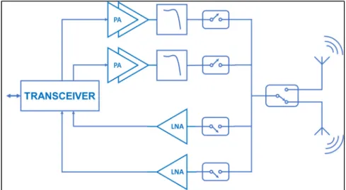
Radio Frequency (RF) switches are a critical building block in many communication systems. These devices can be used in a wide variety of fields, including aerospace, defense, automotive, military, networking & wireless infrastructure. RF switches are especially important in handheld devices (cell phones, tablets, etc.), and an example of their implementation within the RF front-end module is shown in Figure 1.1. There are three main types of RF switches, namely: SPST (Single-Pole Single-Throw), SPDT (Single-Pole Double-Throw), and MPMT (Multiple-Pole Multiple-Throw), the classification being based on the number of inputs and the number of outputs of the particular switch architecture under consideration.
Figure 1.1 RF Switches in Frond-End Module
Various millimeter-wave switches have been designed and reported with good performances on different processes. As an example, reference may be made to a 60GHz switch design using GaAs pHEMT technology and with low insertion loss and high isolation (Lin et al., 2004). In
the same 60GHz frequency band, the asymmetric switch has been demonstrated to have an insertion loss and isolation of 1.9dB and 39 dB, respectively (Byeon & Park, 2013). However, SOI is the technology of preference for most designers to achieve low cost, excellent performance, and low power designs. Examples of such SOI switches include the low insertion loss SPDT switch operating from DC to 60GHz shown in (Parlak & Buckwalter, 2011) and the 1W, 0.9dB insertion loss, millimeter-wave switch shown in (C. Li, Freeman, et al., 2017).
In this thesis, the implementation of millimeter-wave switches working in 28GHz with low insertion loss, high isolation, and linearity is demonstrated. The proposed switches are designed in CMOS SOI 45nm technology from GlobalFoundries. Chapter 2 focuses on the physical structure of the SOI technology process and its benefits. Then, chapter 3 presents the switch parameters, the associated design procedure, as well as some techniques aimed at improving the performance of the switch. Chapter 4 describes the switch designs carried out during this research work, including results from rigorous post-layout simulations. In chapter 5, results from on-wafer measurements of the switches are presented. The final section summarizes the work presented in this thesis and puts forth some conclusions.
1.2 Summary of performances published in the literature
Table 1.1 Summary of published performances
Ref. Frequency (GHz) Insertion Loss (dB) Isolation (dB) P1dB (dBm) Technology Topology [1] 2.5-5 <1 <46 12 0.25μm SOI SPDT Series-Shunt [2] DC-60 <3 >25 - HEMT SPDT Traveling-wave, shunt
5 Ref. Frequency (GHz) Insertion Loss (dB) Isolation (dB) P1dB (dBm) Technology Topology [3] DC-60 <2.5 >25 7.1 45nm SOI SPDT Series-Shunt [4] 50-67 1.9 >38 10 90nm CMOS Unbalanced DS/MN [5] DC-30 <0.8 23 29 45nm SOI SPDT Series-Shunt [6] DC-50 <2.1 >27 10.5 0.13μm SOI SPDT Series-Shunt
Table 1.1 shows the state-of-the-art performances published in the literature in different technologies and topologies. The table also indicates that the SOI technology allows good performances in millimeter-wave switch designs, which is explained in Chapter 2. The author and publishing information about the references in Table 1.1 are listed below, full details are in Bibliographical References Section.
1) C. Tinella, J. M. Fournier, D. Belot, and V. Knopik, "A high-performance CMOS-SOI antenna switch for the 2.5-5-GHz band," IEEE Journal of Solid-State Circuits.
2) K. Y. Lin, T. Wen-Hua, C. Ping-Yu, C. Hong-Yeh, W. Huei, and W. Ruey-Beei, "Millimeter-wave MMIC passive HEMT switches using traveling-wave concept," IEEE Transactions on Microwave Theory and Techniques.
3) M. Parlak and J. F. Buckwalter, "A 2.5-dB Insertion Loss, DC-60 GHz CMOS SPDT Switch in 45-nm SOI," in 2011 IEEE Compound Semiconductor Integrated Circuit Symposium.
4) C. W. Byeon and C. S. Park, "Design and Analysis of the Millimeter-Wave SPDT Switch for TDD Applications," IEEE Transactions on Microwave Theory and Techniques. 5) C. Li, B. Ustundag, A. Kumar, M. Boenke, U. Kodak, and G. Rebeiz, "< 0.8dB IL 46dBm
OIP3 Ka band SPDT for 5G communication," in 2018 IEEE 18th Topical Meeting on Silicon Monolithic Integrated Circuits in RF Systems (SiRF).
6) B. Yu et al., "Ultra-Wideband Low-Loss Switch Design in High-Resistivity Trap-Rich SOI With Enhanced Channel Mobility," IEEE Transactions on Microwave Theory and Techniques.
1.3 Design objectives
The work in this thesis was carried out in collaboration with Skyworks to investigate various millimeter-wave switch structures. Both SPST and SPDT were investigated as a part of this thesis. However, only the SPDTs were the main designs and were designed to be taped-out. And the proposed architecture, with the PA, the LNA, and the RF/mm-wave switch is shown in the figures below.
Figure 1.2 The architecture under investigation with SPST Switch
In this proposed architecture, the power amplifier (PA) and low noise amplifier (LNA) are controlled by the enable bit, as shown in Figure 1.2. In Transmit (TX) mode, the PA is enabled, and the PA’s output signal is transmitted to the antenna through an on-chip metal trace; the SPST switch is OFF during this TX mode (as illustrated in Figure 1.2). In Receive (RX) mode, the PA is turned OFF using the enable bit, with its output impedance being very high. In this mode, the received signal is transferred from the antenna to the input of the LNA through the SPST switch, which is turned ON. The key aspect of the application context illustrated in Figure 1.2 is that the insertion loss in the TX path must be minimized, with the SPST in the OFF state offering a high impedance at its antenna terminal while providing maximum isolation between the PA output and the LNA input. Also, in the RX mode, the insertion loss
7
through the SPST must be minimized for noise figure considerations. Therefore, to exploit the full benefits of this architecture, the SPST switch in Figure 1.2 has to be designed to provide high impedance, high isolation and excellent linearity when turned OFF, and low insertion loss when turned ON.
An alternative architecture with an SPDT switch is shown in Figure 1.3. For the SPDT switch, the insertion loss for the TX path has to be lower than the insertion loss in the RX path while the isolation of the RX path (from Antenna to LNA input) has to be higher than the isolation of the TX path (from PA output to Antenna).
Figure 1.3 Alternative architecture with an SPDT Switch
These and other designs constraints translate into specifications for the RF switches that are summarized below:
• Center frequency: 28GHz,
• Minimum insertion loss for the TX path: IL < 1dB at 28GHz, • Good isolation on both TX and RX path: ISO > 20dB,
1.4 Context of research
This research was part of an NSERC-CRD funded project, involving a collaboration between Professor Constantin and Skyworks Solutions Inc. It is important to note that this research was conducted with a very tight schedule from specifications release to prototype chip fabrication. However, for unforeseen reasons related to business operations at GlobalFoundries, there was a cumulative one-year delay in the IC tape-out and manufacturing. Additionally, the tests for the designs in this thesis started in Feb 2020 but had to prematurely stop two weeks later due to the limited time available for tests.
It is also worthwhile to note that we are constrained regarding the amount of technical data related to the fabricated switch and designs that can be provided in this thesis, due to restrictions about disclosing proprietary content from Skyworks Solutions, Inc. as well as from GlobalFoundries.
1.5 Contributions to research
The contributions of the work presented in this thesis to the area of RF/mm-wave switches are summarized below:
• Thorough simulations were carried out for an in-depth study of existing switch designs.
• The study, design, and measurement of four different SPDT switch topologies were accomplished and were useful for the system-level Tx-Rx chip design.
• The switches were designed and successfully tested at 28GHz. The measured performances comply with our initial requirements for new mm-wave Tx-Rx architecture under investigation. Therefore, this research work has contributed to the portfolio of successful switch designs using the 45nm CMOS SOI process from GlobalFoundries (GF) and
9
provides important insight into the range of performances that can be achieved using the GF 45nm CMOS SOI process.
The asymmetric SPDT switch achieved excellent performances at 28GHz, compliant with specifications, with the measured insertion loss from the TX to the Antenna being smaller than 1dB and the measured isolation between TX and RX being ~28dB.
CHAPTER 2
KEY PRINCIPLES OF MILLIMETER-WAVE SWITCH DESIGN
2.1 SOI Process
2.1.1 Physical Structure of SOI
The Silicon-On-Insulator technology (SOI) concept was proposed by C.W. Miller and P.H. Robinson in 1964 and first commercialized in 1995. The cross-section of a typical SOI NMOS transistor is shown in Figure 2.1 below.
Gate
Body
Buried Oxide (BOX)
D S
STI STI
Silicon Substrate
Figure 2.1 Cross-section of SOI NMOS
As seen in Figure 2.1, the main difference between SOI CMOS and Bulk CMOS structure is the Buried Oxide (BOX) layer. This insulator layer separates the active silicon layer from the underlying silicon substrate. The BOX layer, therefore, significantly reduces the parasitic junction capacitances that exist between the source and the substrate, and between the drain and the substrate, when compared to the Bulk CMOS structure, resulting in better high-frequency performance. Moreover, the BOX layer also blocks unwanted signal leakage into the semiconducting silicon substrate, which reduces the power loss.
Buried Oxide (BOX)
G
S
D
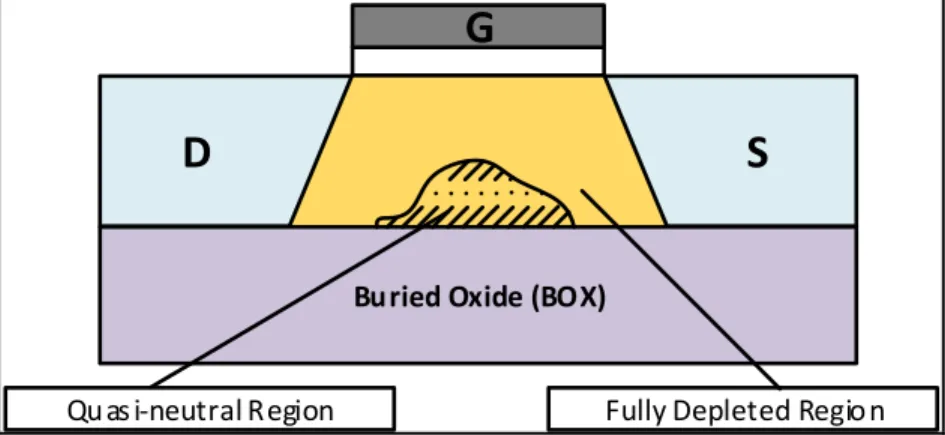
Qu as i-neutral Region Fully Depleted Regio n Figure 2.2 Cross-section of Partially Depleted (PD) SOI
There are two types of SOI devices: Fully Depleted (FD) SOI and Partially Depleted (PD) SOI. Figure 2.2 shows the structure of PD SOI, which has an undepleted part of the silicon film under the channel when the device is conducting. When the MOSFET is called fully depleted, it means the entirety of the active silicon film is depleted during conduction. FD SOI devices use a thinner active silicon film than PD SOI devices.
In this context, it is worth comparing the PD SOI device with the FD SOI device to understand which SOI device is more suitable for a particular application. Table 2.1 below compares some characteristics of PD SOI and FD SOI devices, and is adapted from the information provided by “The SOI Industry Consortium – A consortium dedicated to the understanding, development, and adoption of SOI-based technologies.”
13
Table 2.1 Comparison of PDSOI device and FDSOI device
PD SOI FD SOI
Structural Differences
• Doped channel.
• Top silicon is 50nm to 90nm thick (referred to as for “thick SOI” applications).
• The insulating BOX layer is typically 100nm to 200 nm thick.
• Often uses undoped or lightly doped channel. • Top silicon is 5nm to
20nm thick.
• The insulating BOX layer may also be ultra-thin i.e. 5nm to 50nm.
Target Applications
• High-performance microprocessors.
• Other applications include embedded design, RF/analog design, automotive sector, power sector,
military/aerospace sector, etc.
• High-performance microprocessors. • Low-power electronics. • Ultra-low-power systems. Advantages • Well understood. • Industrially qualified. • Easier to manufacture. • It can leverage the floating
body for performance gain and memory applications.
• Current leakage and power consumption are drastically reduced. • Random fluctuations in
Vt minimized for undoped channels. • No floating body effect;
easier to control short-channel effects.
PD SOI FD SOI
Challenges
• Physical limits to scalability are approaching for high performance.
• New metrology needed for defect detection in very thin layers.
• Vt defined by gate work function and intrinsic body.
• The very thin body can be challenging to manufacture and for implementing
performance boosters.
Nodes
• 180nm to 22nm channel length.
• 22nm and lower channel length for
high-performance
microprocessors and low-power electronics.
For the GlobalFoundries45RFSOI process used for fabricating the switch designs described in this thesis, only PD SOI devices are available.
2.1.2 Benefits of GlobalFoundries 45RFSOI process for RF Switches
The GlobalFoundries 45RFSOI has been demonstrated to offer excellent performance for FEMs (Front-End-Modules), including for the design of LNA, PA, and Switches at high frequencies (μWave and mm-Wave). To evaluate the high-frequency performance of RF transistors, fT and fMAX are used as key indexes that are used. The term fT refers to the frequency when the current gain of the device drops to unity under AC shorted output conditions. The term fMAX refers to the frequency when the power gain of the device drops to unity under
15
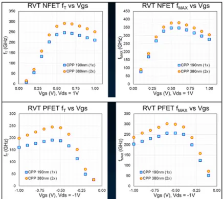
conjugate matched input and output conditions. For the GlobalFoundries 45RFSOI process, reference may be made to (A.Rabbeni, 2017), which shows that the fT and fMAX for the transistor in this process (using a device with L=40nm, W=20μm) are among the best in their category for comparable technologies. Performances for various biasing conditions are shown in Fig 2.3.
Figure 2.3 NFET and PFET fT/fMAX performance of GlobalFoundries 45RFSOI process
Taken from A.Rabbeni (2017, p.14)
In the 45RFSOI process, Global Foundries introduced significant performance improvements through the high-resistivity trap-rich substrate. (Tinella, Fournier, Belot, & Knopik, 2003) demonstrated the advantages of using high-resistivity (HR) substrate to reduce the losses in the RF switch design. However, (Lederer, Lobet, & Raskin, 2004) indicated that the HR SOI is still affected by the parasitic surface conduction, which degrades the effective resistivity and increases the substrate losses. These losses may be traced to the high fixed charges within the oxide layer attracting free carriers near the substrate interface. The trap rich layer was introduced between the interface of the BOX layer and the HR Si substrate to capture the free
carriers near the substrate interface, resulting in improved effective resistivity and linearity( (Ali, Neve, Gharsallah, & Raskin, 2011), (Neve & Raskin, 2012) and (Yu et al., 2017)).
It is worthwhile to note that GlobalFoundries provides two types of RF FETs in the 45RFSOI process: Thin-Oxide FET and Thick-Oxide FETs, with different values of device length. Thick-Oxide FETs with longer device lengths help to increase the breakdown voltage. Such a breakdown may occur due to a variety of reasons such as punch-through breakdown, gate-oxide breakdown, etc. as described in Section 2.2.3. A higher breakdown voltage means that designers can design the high-power RF switch with a smaller number of stacked FETs, as presented in Chapter 4 of this thesis.
2.2 Key switch parameters
2.2.1 S-Parameter of Switches
In (Pozar, 2012), Insertion Loss (IL) for a switch is defined by the ratio of the output power Pout to the input power Pin. It is a measure of the power loss when the signal goes through the switch, and it is defined as shown in (2.1).
( ) 10 log out in P Inserrtion Loss dB P = (2.1)
In a known impedance system (e.g., 50Ω), Insertion Loss is also equivalently defined by the voltage attenuation, as shown in (2.2), where Vout and Vin refer to the input and output voltage values respectively.
( )
20log out in V Insertion Loss dB V = (2.2)17
During the simulation, this parameter is specified by the S-Parameter value S21 of a two-port network. For switches, the insertion loss is measured in ON-state when the signal is intended to go through it. It is worthwhile to note that in the ON-state, the switch is equivalent to a small resistor that causes a small amount of power loss.
The Isolation (ISO) of the switch is specified using the S-Parameter value S21 measured when the switch is OFF, i.e. when the input signal is intended to be blocked by the switch from going to its output.
The Return Loss (RL) of the switch is defined by the ratio of the reflected power Pref and the incident power Pin as defined in (2.3).
( )
10 log ref in P RL dB P = (2.3)This parameter indicates how well the switch is matched with the port (e.g. 50 Ohm). A high return loss value indicates a well-matched system and vice versa.
2.2.2 Linearity
As an active circuit, the linearity of RF switches is a critical parameter. This parameter indicates the degree of nonlinearity in the relationship between the input and output signals. Ideally, the output signal of the switch varies linearly with its input signal for the entire range of power levels for which application the switch is designed. However, this is not the case in reality, and switch nonlinearity can result in unwanted performance impairments, especially at higher power levels. The 1dB compression point P1dB is a useful and convenient metric in simulations and measurements to characterize device linearity.
The 1dB compression point P1dB is defined at either the input node or the output node of the switch as the power level where the insertion loss increases by 1dB from its small-signal value. It is useful to remind that small-signal values refer to the operation regime where the switch excitation power levels are very low.
Pin (dBm) 5 10 15 20 25 30 35 In se rt io n L o ss (d B ) 1dB P1dB
Figure 2.4 The 1dB Compression Point P1dB
The work in (Steven Belletete, 2009) shows that the switch’s compression point depends on the performance of the process that is used, the design topology, the bias control voltage, and the operating frequency. The 45RFSOI process used in this thesis has an excellent performance of linearity, thanks to the improvements in its physical structure, namely regarding the high resistivity substrate, as discussed in Section 2.1.2. Moreover, the stacking-FETs topology, as presented in Section 3.1, also helps to increase the P1dB of the switch.
It is useful to understand the dynamics behind the onset of compression in FET switch designs, an excellent explanation of which is given in (Devlin, 1999). For the ON state case, the current flowing through the switch depends on the RF voltage, and compression occurs when the peak RF current (Ipeak) is higher than the saturation current (Idss) of the FET, resulting in signal clipping. On the other hand, there is a small amount of leakage current that passes through the switch when the switch is OFF. In this scenario, the high RF voltage swing can result in device breakdown. This aspect is discussed in Section 2.2.3, while design methods to avoid the breakdown in switches are described in Chapter 4.
19
2.2.3 Breakdown Voltage
In general, four primary sources cause the breakdown of a FET device, namely:
• Gate-Oxide breakdown: This effect occurs because of the high Gate-Drain voltage swing, which results in the electrons tunneling from the conductive channel into the oxide area under the gate. These carriers degrade the quality of the oxide layer slowly and lead to catastrophic failure of the oxide over time.
• Punch-through: For short channel devices, the large Drain-Source voltage can damage the FETs through punch-through effects. Punch-through effects arise when the device channel length becomes shorter, and the depletion region around the drain and source overlap with each other. As a result, the gate voltage loses its control over the operation of the FETs to the drain voltage, allowing excess current flowing within the silicon layer below the normal conduction channel (hence the term punch-through) and resulting in unwanted performance impairments.
• Hot electron effects: As the Drain-Source voltage gets higher, the electrons in the Si-film are accelerated. When these electrons acquire an adequately high speed (hot), they slam against the gate oxide. These electrons may then travel through the gate oxide into the gate node, causing degradation of the gate oxide and changes in the threshold voltage. This phenomenon results in unwanted performance impairments referred to as hot-electron (or hot-carrier) effects.
• Avalanche breakdown: This effect occurs when the Drain voltage increases considerably, resulting in an increased reverse bias voltage across the Drain-Gate nodes and, consequently, an increased value of the resulting reverse-biased electric field. The minority carriers that cross the depletion region are accelerated under the electric field. When these carriers gain enough energy, they can break covalent bonds in atoms that they collide with (ionization collision). Each freed carrier created by this process may have enough energy
to be able to cause another collision, thereby, creating even more free carriers, in a chain reaction-type mechanism. This effect occurs in the fashion of an avalanche, generally resulting in a catastrophic failure of the device.
CHAPTER 3
RF SWITCH DESIGN TECHNIQUES
In this chapter, the techniques underlying the design of four different switch variants (asymmetric SPDT, symmetric SPDT NMOS, symmetric SPDT PMOS, and asymmetric SPDT with Cross Biasing) are discussed. These variants themselves are presented in greater detail in Chapter 4.
3.1 Stacking FETs
As explained in the previous Chapter, the MOSFET breakdown voltage is an important parameter that should be considered carefully in the RF switch design. Stacking FETs is the most straightforward approach to overcome this issue (Devlin, 1999). (Zhu et al., 2015) states that the total voltage across the stack is distributed equally between the individual members of the stack. Therefore, the breakdown voltage of the stack can be calculated using equation (3.1) below.
FET
BV nBV= (3.1)
where BVFET is the breakdown voltage of a single FET and n is the number of FETs in the stacked FET.
However, (Zhu, Klimashov, & Bartle, 2014) demonstrated that “the voltage across the FET stack is not equally divided,” which means that the breakdown voltage BV across the FET stack is not a linear function of n, the number of stacked FETs. Therefore, selecting too large a value of n does not offer a proportionately larger value of breakdown voltage BV, which tends to saturate after a certain value. This suggests that n should not be indefinitely increased to be too large.
Moreover, the larger number of stacked FETs can improve the power compression characteristics of the switch, given the lower Drain-Source and Gate-Drain voltage swings in OFF-state (Devlin, 1999), granted that the device sizes are large enough to allow higher saturation current Idss in ON-state.
However, increasing the number of stacked FETs causes a larger value of its ON-resistance. This translates into a worse value of insertion loss, while offering better isolation. The topology presented in section 3.2 helps to increase isolation while maintaining the insertion loss of the switch.
Input
Output
R
ONFigure 3.1 Stacked FETs with equivalent ON-resistance RON
A series stacked FETs structure, as shown in Figure 3.1, is simulated in the time domain with the number of FETs n set to 3, to demonstrate better the effect of stacking FETs. The RF signal applied at the Input port results in a power level of 20dBm at the Output port. Note that the Output node is referred to as the Drain node without any loss of generality, since the MOS Switch is a symmetrical device. The corresponding voltage swing for a single member of the three-stack switch is checked at the Drain, and the Source node in two states (ON/OFF), respectively, and shown in Figure 3.2.
23
Figure 3.2 The voltage swings at the Drain and Source nodes in the ON and OFF states
In Figure 3.2, it can be seen that the peak of the voltage swing at the Drain (green curve) and Source (pink curve) terminals of a single FET are nearly identical in the ON state (VD -VS=150mV). On the contrary, the peak of the Drain-Source (green and blue curves) differential voltage swing is about 1.1V in the OFF state. Such a voltage swing in the OFF state can cause MOSFET breakdown if it is too large. Therefore, the number of FETs has to be selected to ensure the switch can survive under signal excitation at the highest power levels that are aimed at for an application.
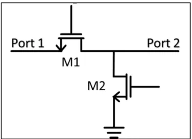
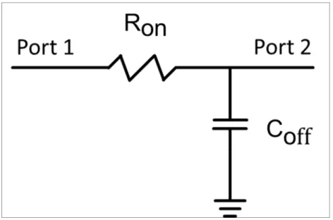
3.2 Series-Shunt Structure
Figure 3.3 The Series-Shunt switch structure
There are several topologies for RF Switches, as mentioned in (X. J. Li & Zhang, 2010). These include variations in the matching-network (He, Xiong, & Zhang, 2012), λ/4 transmission lines (Uzunkol & Rebeiz, 2010), traveling-wave (Chao, Wang, Su, & Chern, 2007), or Unbalanced Double Shunt/Matching Network (Byeon & Park, 2013). These topologies have been shown to exhibit good performances for RF switches at high frequencies. However, these designs all require λ/4 transmission lines, which are not a problem in terms of size for very high-frequency applications (higher than 40GHz). In this thesis, the switches are designed to operate at 28GHz; hence the topologies referenced earlier are not suitable, given that the chip area for RF switches is too limited, according to our integration requirements.
The Series-Shunt Topology is a good choice for RF Switch design in this work. Several designs with good performances have been described in the literature, such as (Lin et al., 2004), (C. Li, Freeman, et al., 2017), (C. Li et al., 2018), (Parlak & Buckwalter, 2011), etc. Coupled with the inherent benefits that stem from the SOI process, the Series-Shunt topology has several attractive advantages for RF Switches. Figure 3.3 shows the schematic of the switch structure using the Series-Shunt topology. The voltage logic control for the Series FETs is the inverse
25
of the logic control for the Shunt FETs. It means that the shunt FETs are OFF while the series FETs are ON, and vice versa.
Figure 3.4 The equivalent switch model in transmitting mode
The small-signal equivalent circuit of the series-shunt topology is now analyzed in the ON (transmitting mode) and OFF (isolation mode) states. As shown in Figure 3.3, M1 refers to the series FETs, and M2 refers to the shunt FETs. Figure 3.4 is the equivalent circuit of the structure in Figure 3.3 when M1 is ON, and M2 is OFF. Under these conditions, the signal is allowed to be transmitted from port 1 to port 2 (or vice versa). The S-Parameter S21 in this mode is a measure of the insertion loss of the switch and identified using the ABCD matrix given by (3.2) below (Yu et al., 2017).
1 . 1 on off on off R j C R A B j C C D ω ω + = (3.2)
By applying the conversion from the ABCD matrix to the S-Parameter matrix, the value of S21 is given by (3.3). Consequently, the value of the Insertion Loss (in dB) of the ON-state switch in Figure 3.4 is given by (3.4).
(
)
21 2 2 on off on o o S R j C R Z Z ω = + + + (3.3)(
)
21 2 2 2 ( ) 20log 10log 1 2 2 off on o on o IL dB S C R Z R Z ω = − + = + + (3.4) where:• Ron is the on-resistance of the series FETs in transmitting mode,
• Zo is the reference impedance (e.g., 50 Ohm) of the source and load,
• COff is the off-capacitance of the shunt FETs in transmitting mode.
In equation (3.4), it is observed that the IL depends on the value of Ron and Coff. The smaller
the values of Ron, Coff, the better is the value of the insertion loss of the switch in transmitting
mode.
27
The isolation of the switch is also calculated in a similar method as above (Yu et al., 2017). For this, the small-signal equivalent circuit of the series-shunt topology in Figure 3.3 is now analyzed in the OFF state (isolation mode). Figure 3.5 is the equivalent circuit of the structure in Figure 3.3 when M1 is OFF, and M2 is ON. Under these conditions, the signal is not allowed to be transmitted from port 1 to port 2 (or vice versa). The S-Parameter S21 in this mode is, therefore, a measure of the insertion loss of the switch and identified using the ABCD matrix given by (3.5) below. 1 1 1 off off C C on on Z Z A B R C D R + = (3.5)
Like the procedure in (3.3), the value of S21 after using the ABCD matrix to the S-Parameter matrix conversion is given by (3.6) below. Consequently, the value of the Isolation (in dB) of the OFF-state switch in Figure 3.5 is given by (3.7).
21 2 1 1 1 2 o on off o on S Z R j Cω Z R = + + + (3.6) 21 2 2 2 ( ) 20 log 1 10 log 1 1 2 2 o o on off o on ISO dB S Z Z R ωC Z R = − = + + + (3.7)
From (3.4) and (3.7), we can see the impact of Ron and Coff on the insertion loss and the isolation of the switch. However, these equations suffer from a lack of accuracy since they do not account for FET parasitic capacitances. These parasitic capacitances have a significant effect at high frequencies. Section 4.1 describes a procedure to find the size of FETs when a given
value of insertion loss and isolation are aimed at 28GHz. In Section 3.3, the floating gate technique and how it helps to reduce the effect of parasitic capacitances are explained.
3.3 Floating Gate
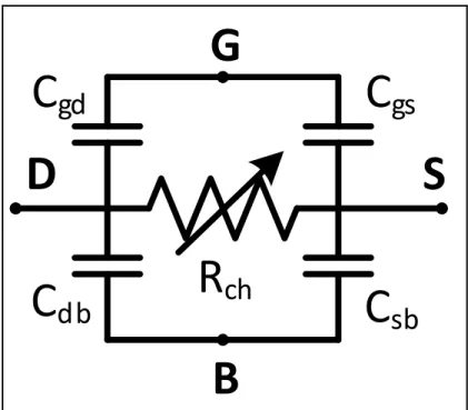
(Devlin, 1999) indicated that a large gate resistor (several kΩ) is the most simple and effective way to improve the isolation between the RF signal and the gate control. (Wang et al., 2014) called this technique the AC-floating technique because the gates are connected to ground only after a series large resistor. To understand this, it is essential to look at the FET device with the various parasitic capacitances included in it. Figure 3.6 is the model of a FET device that accounts for parasitic capacitances between the Gate, Source, Body, and Drain nodes. At high frequencies, the RF signal can leak from the drain to the gate through the parasitic capacitors Cgd or Cgs. By using a large series gate resistor, the signal leakages through the gate are significantly reduced, resulting in reduced losses.
G
B
D
S
C
gd
C
gs
C
sb
C
db
R
ch
29
(Tinella et al., 2003) also demonstrated that the floating-gate technique helps to reduce insertion loss but offered an alternate explanation. This explanation is because without a large gate resistor Rg, the control voltage Vgs depends on the voltage signal swing at the Source node of the FET. A large signal swing at the Source can lead to the fluctuation of channel resistance Rch, thereby increasing signal losses. With a large value of the series gate resistor Rg that collects the voltage swing, the voltage Vg is kept nearly at a constant value during the signal period. This means that the channel resistance Rch does not depend significantly on the input signal anymore, which helps to reduce losses.
CHAPTER 4
28GHz SWITCH DESIGNS
4.1 SPST (Single Pole Single Throw)
The first switch topology that is presented is the Single Pole Single Throw (SPST). Although no switch design with this topology was taped-out as part of this Master's research, its structure was the starting point for investigating the performances of all the Single Pole Double Throw (SPDT) topology variants discussed subsequently. The SPST topology also considerably simplifies the discussion on the compromises associated with the structure of a switch design.
Recalling what was discussed in chapter 3, the transistors in series perform the main ON/OFF switch function while the shunt transistors are used to improve the isolation of the switch. Therefore, the very first step of designing an SPST is to determine the number of transistors N in series to overcome the breakdown voltage issue. We reiterate equation (3.1) below, where the value of N is based on the peak value of the input voltage swing i.e.
𝑉 = 𝑁 × 𝐵𝑉𝑑𝑠 (4.1)
where:
• Vpeak: the peak value of the voltage swing of the input signal, • N: the number of stacked FETs in series,
• BVds: the breakdown voltage Vds of a single FET.
For example, an input power of approximately 20dBm for 50Ω system under VSWR =1:1 condition translates into a peak voltage swing of 3.162V. From the PDK documents of GlobalFoundries, the maximum Vds for RF FETs in their 45nm CMOS SOI process at 125oC is 1.1V. Therefore, to absorb the 3.162V peak voltage swing, the value of N must be at least three.
As mentioned in Chapter 3, the SPST switch topology uses a series-shunt structure. Once the minimum value of N is determined, the sizes of the transistors comprising the SPST need to be optimized for values of insertion loss and isolation that meet targeted specifications. According to (Tinella et al., 2003), the resistance of the series transistors at low frequencies is the primary contributor to switch losses. By enlarging the width of the series transistors, the low-frequency insertion loss in the ON state can be improved significantly. However, such an increase in the width of the transistor causes an increase in its capacitive parasitic, hence degrades isolation given the reduced impedance and increases the leakage current through the transistor in the OFF state. These effects become more significant at higher frequencies. This means that there is an optimum value for the gate width at a given frequency, which offers the desired compromise between insertion loss and isolation to meet the targeted switch specifications.
RG
Input Output to LNA
RG VG1
VG2 To ATN
Figure 4.1 The SPST schematic
Figure 4.1 shows the schematic of the SPST switch with three stacked FETs in series/shunt structure. The gate voltages are set to +1V to turn ON the transistors or set to -1V to turn them OFF. The biasing resistors RG are selected to have a high value of 10 KΩ, this value being chosen for an acceptable compromise between the insertion loss and the switching time (Parlak
33
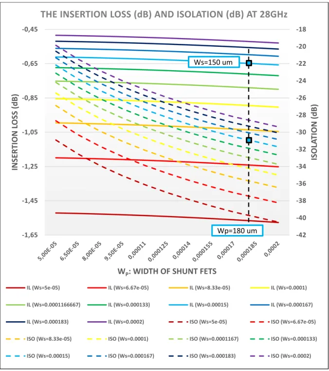
& Buckwalter, 2011). Thereafter, the width of the series FETs (Ws) and the shunt FETs (Wp) are swept within the simulation environment to find the optimum values at 28GHz, which offers the right trade-off between insertion loss and isolation. The results of this simulation for the SPST switch of Figure 4.1 is shown in Figure 4.2. Here, the widths Ws and Wp are varied from 50μm to 200μm. The insertion loss values (solid lines) are almost flat along the horizontal axis because of the relative independence of the insertion loss value with respect to the shunt FETs width Ws. On the other hand, the isolation values (dashed lines) increase significantly with the width Ws of the shunt FETs. Ultimately, the targeted requirements of the SPST switch determine the values of Ws and Wp that are chosen for any given application.
For the targeted application in this thesis, the sizes of the devices shown in Table 4.1 were selected to allow achieving an insertion loss lower than 1dB and isolation higher than 30dB at 28GHz. This is confirmed via SP simulation at 28GHz, the results of which are shown in Figure 4.3. Note that all simulation results shown in this thesis are performed within the CadenceTM design environment.
Table 4.1 Device sizes for SPST design of Figure 4.1
Series FETs W/L=150μm/40nm RF NMOS Floating Body
Figure 4.2 Plot shows the variation of insertion loss (full curves) and isolation (dotted curves) as a function of the width (units in m) with the length fixed at 40nm,
for series and shunt FETs in SPST topology.
This plot is used to determine the optimum width values of the FETs
-42 -40 -38 -36 -34 -32 -30 -28 -26 -24 -22 -20 -18 -1,65 -1,45 -1,25 -1,05 -0,85 -0,65 -0,45 ISOLA TION (dB) INSER TION L O SS (dB)
WP: WIDTH OF SHUNT FETS
THE INSERTION LOSS (dB) AND ISOLATION (dB) AT 28GHz
IL (Ws=5e-05) IL (Ws=6.67e-05) IL (Ws=8.33e-05) IL (Ws=0.0001) IL (Ws=0.0001166667) IL (Ws=0.000133) IL (Ws=0.00015) IL (Ws=0.000167) IL (Ws=0.000183) IL (Ws=0.0002) ISO (Ws=5e-05) ISO (Ws=6.67e-05) ISO (Ws=8.33e-05) ISO (Ws=0.0001) ISO (Ws=0.0001167) ISO (Ws=0.000133) ISO (Ws=0.00015) ISO (Ws=0.000167) ISO (Ws=0.000183) ISO (Ws=0.0002)
Ws=150 um
35
Figure 4.3 The SPST switch S-Parameter performance from 24GHz to 30GHz
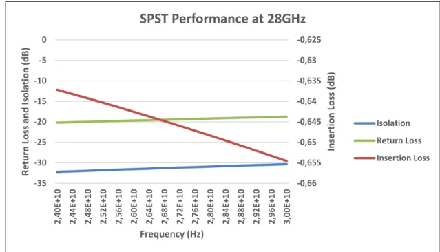
From 24GHz to 30GHz, the insertion loss of the SPST is approximately 0.66 dB, the isolation is higher than 30dB, and the return loss is larger than 18dB. The power sweep in Figure 4.4 shows that the value of the 1dB compression point P1dB of the SPST is about 28dBm. These figures satisfy the requirements for the SPST switch design.
The SPST switch is only simulated using its schematic design because it was not the final design that was taped-out due to reasons beyond the scope of this thesis. However, these simulated results of this SPST form the basis for benchmarking the performances of other switch designs that are discussed subsequently in this thesis. Additionally, an optimization routine similar to that discussed so far for the SPST switch is used to determine the FET widths of the different SPDT switch variants whose layouts were designed in CadenceTM. Note that for these switch designs with layouts, the simulations presented include a full EM simulation of the layout passives (including the signal pads) using EMXTM tool. The full post-layout simulations shown are performed using this EM extraction file as well as appropriate models for the active circuits (FETs) in the design. The parasitic of the pads, the inductors and the metal ground contribute insignificant loss into the total performance of the switch.
-0,66 -0,655 -0,65 -0,645 -0,64 -0,635 -0,63 -0,625 -35 -30 -25 -20 -15 -10 -5 0
2,40E+10 2,44E+10 2,48E+10 2,52E+10 2,56E+10 2,60E+10 2,64E+10 2,68E+10 2,72E+10 2,76E+10 2,80E+10 2,84E+10 2,88E+10 2,92E+10 2,96E+10 3,00E+10
Frequency (Hz)
Insertion Loss
(dB)
Return Loss and
Isolation (dB)
SPST Performance at 28GHz
Isolation Return Loss Insertion LossFigure 4.4 Gain Compression vs. Pin plot to determine the P1dB of SPST switch
In summary, a good SPST has to provide low insertion loss from the Antenna (ATN) port to the signal port (going to the PA or the LNA) when it is ON (i.e. have a low RON) while minimizing the signal leakage when it is OFF (i.e. have a low COFF). These performance metrics inherently impose the following design compromises in an SPST switch design:
• Achieve low RON: Increase W/L of FETs; Reduce the Number of FETs in an arm, • Achieve low COFF: Reduce W, increase L of FETs; Increase Number of FETs in an arm.
4.2 SPDT (Single Pole Double Throw)
The SPDT was determined to be the topology of choice for the system of Figure 1.3 and was ultimately designed and taped out. This architecture incorporates a Power Amplifier and a Low Noise Amplifier connected to the common Antenna through an SPDT. The design flow for the design of the SPDT switch consists of first designing the Symmetric NMOS SPDT and the Symmetric PMOS SPDT variants. Thereafter, the Asymmetric SPDT variant is designed to achieve a smaller insertion loss in the TX path and higher isolation in the RX path. However,
-2,5 -2 -1,5 -1 -0,5 0 0 5 10 15 20 25 30 35 Gain Compression (dB) Pin (dBm)
Gain Compression
37
the Asymmetric SPDT requires the use of a negative voltage generator (NVG) to achieve good performance. The requirement to use an NVG is circumvented through the use of Cross Biasing in the Asymmetric SPDT design. These design variants are discussed sequentially in the sections that follow.
4.2.1 Asymmetric SPDT
The design procedure for an SPDT switch is similar to that of an SPST switch, and with similar performance compromises between insertion loss and isolation along a switching arm. In general, the SPMT (Single-Pole Multi-Throw) switch with T number of throws has more insertion loss in comparison with the SPST switch, the insertion loss becoming more as the number of throws T becomes higher. This is because when any single arm is ON, isolation through the T-1 OFF arms is optimized by reducing the value of their COFF, as seen in Figure 4.5 below. As shown earlier, sizing the transistors to reduce COFF leads to a larger RON, hence resulting in higher insertion loss. As a result, the dimensions of the SPDT switch have to be re-optimized compared to the original SPST switch.
RON COFF 1 2 Antenna Port COFF T
TX Port VG1 VG2 RX Port VG1 VG2 ATN Port
Figure 4.6 The schematic of the asymmetric SPDT switch
Figure 4.6 shows the schematic for the asymmetric SPDT switch. The gate voltages are set to +1V to turn ON the transistors or set to -1V to turn them OFF. As mentioned in (Byeon & Park, 2013), an asymmetric SPDT switch includes two arms with non-identical topologies. The TX arm for an asymmetric SPDT switch is designed with matching-network topology, resulting in a low insertion loss but also low isolation (Uzunkol & Rebeiz, 2010). On the other hand, the RX arm for an asymmetric SPDT switch is an SPST switch with a traveling-wave topology (including a transmission line) that has high isolation and, consequently, a higher insertion loss (Schindler & Morris, 1987). After comparison, it was determined that for the design in this research, both the TX and the RX arms of the asymmetric SPDT would use the same series-shunt structure without transmission line, as presented earlier. The primary motivation behind the series-shunt structure is that it helps to reduce the overall switch dimensions size, and hence affords better integration in FEM architecture. Of course, the performance specifications for a required application ultimately drive the choice of switch topology to be used.
39
For the current asymmetric SPDT switch design illustrated in Figure 4.6, thin-oxide RF NMOS FETs (inside blue circles) are used for the TX side, and thick-oxide RF NMOS FETs (inside red boxes) are used for the RX side with regard to the series transistors. The reason for using thick-oxide FETs in the RX arm is that in TX mode when TX is ON, and RX is OFF, the high-power signal from the PA goes through the thin-oxide RF NMOS switch with a low voltage drop but results into a high voltage across the thick-oxide RF NMOS FETs in the RX arm. The series FETs within red boxes in the RX arm (which are in OFF state) must therefore have higher breakdown voltage to make sure that the VDS of each FET (where VDS=Vpeak/N) is lower than the breakdown voltage BV of a single FET device. Following this, the dimensions of the Asymmetric SPDT are optimized by simulations. Table 4.2 shows these optimum values (determined from similar plots as those in Figure 4.2) for the dimensions of the asymmetric SPDT FETs. Note that the TX arm uses 40nm FETs, while the RX arm uses 112nm FETs.
Table 4.2 The dimensions of the asymmetric SPDT
Series FETs Shunt FETs
TX arm W/L=224μm/40nm W/L=120μm/112nm
RX arm W/L=210μm/112nm W/L=162μm/40nm
Once the optimum FET dimensions are determined by simulation, the switch layout is designed while accounting for the signal pads, the ground pads, and the dc signals pads. Note that the pitch from the center-to-center of adjacent pads is 150µm.
Figure 4.7 Layout of the asymmetric SPDT
Figure 4.7 shows the layout for the asymmetric SPDT with three RF G-S-G (Ground-Signal-Ground) pads, intended for on-chip measurements with a probe station. These three G-S-G pads are for the RF signals at the ANTENNA port, the PA port, and the LNA port. Ports G1 to G6 refers to the ground pads of the G-S-G probes. Multiple DC pads are also included for biasing and are present on the right side in Figure 4.7.
Table 4.3 The asymmetric SPDT Performance
TX MODE RX MODE
Insertion loss (dB) < 0.7 < 1.5
Isolation (dB) > 27 > 24
Return Loss (dB) > 12 > 15
41
Table 4.3 shows the post-layout simulation performance results of the SPDT switch over the frequency range from 24GHz to 30GHz. As may be seen in the table, the TX arm has a higher weight associated with its insertion loss (<0.7dB), its isolation (>27dB), and linearity (P1dB=28dBm). The RX arm has a better value of return loss (>15dB). These simulated results satisfy the specifications for the targeted application.
4.2.2 Asymmetric SPDT with Cross Biasing
A negative voltage generator is required for switches that utilize the negative biasing method. Incorporating a negative bias to turn OFF the devices, as in the previous design of asymmetric SPDT shown in Figure 4.6, has shown through simulations that it affects positively the switch performance, by shifting down the voltage swing of VGS, VGD. In that way, the large voltage swing cannot go higher than the threshold voltage, avoiding the undesired turning-on of the OFF-state FETs. For such implementations, negative voltage generators and control circuits are normally required, and that include an oscillator with clock buffers, a charge pump, a low-pass filter, and level shifters (Chaudhry, Bayruns, Arnold, & Sheehy, 2012).
(Im, Kim, Im, & Lee, 2015) demonstrated the drawbacks associated with using negative voltage generators for the design of switches. Due to the use of multiple circuit blocks (oscillator, charge pump, etc.), the structure of FEMs with such switches are inherently more complex. Additionally, the fluctuation of the turn-on voltage depends on the switching nature of the charge pump, and this has an adverse effect on the noise in the RF signal (Cha, 2010). To circumvent the issues mentioned above, an SPDT switch with the cross-biasing technique is now introduced.
For an SPDT switch with the cross-biasing technique, instead of using a negative voltage for the FET gate, the gate-to-source and gate-to-drain voltage of the ON and OFF branches of the switch is applied using an alternative biasing method. This is equivalent to using the negative voltage. To understand this alternative biasing method better, refer to Figure 4.8. Let us assume that the TX arm is ON and the RX arm is OFF. VG1 is then set to 1V and VG2 to 0V. The DC
value of the VGS of the series FET on the TX (ON) arm is, therefore, VG1-VG2=1V, while the DC value of the VGS of the series FET on the RX (OFF) arm is VG2-VG1=-1V. Similarly, the DC value of the VGS of the shunt FET on the TX (ON) arm is -1V, while the DC value of the VGS of the shunt FET on the RX (OFF) arm is 1V. Such a cross-biasing technique, therefore, effectively replicates the use of negative biasing.
RX Port VG1 VG2 ATN Port VG1 VG1 VG2 VG2 TX Port VG2 VG1
Figure 4.8 Schematic of the asymmetric SPDT switch with cross biasing
However, the cross-biasing method requires using large dc-block capacitors between the switch arms and the ports, as shown with red-colored capacitors in Figure 4.8. The purpose of the DC-Block capacitors is to prevent DC leakage current through the switch. The use of these large capacitors adds more loss to the total insertion loss of the switch, because on-chip capacitors are inherently lossy components. The capacitance value has to be optimized to reduce its impact on the insertion loss at the targeted frequency. Smaller capacitance values increase insertion loss, while large capacitance values increase the size of the switch.
In a separate simulation set-up with a series-stack of three FETs and dc-block capacitors, a full two-port S-Parameter analysis was performed to evaluate this insertion loss.
43
Figure 4.9 IL Simulation of the series-stacked FETs at 28GHz versus the capacitance values
Figure 4.9 shows the simulation of the insertion loss of the series-stacked FETs versus the capacitance value of CBLOCK. As illustrated, to keep the insertion loss at 28GHz close to 0.5dB (0.5dB being the value of the insertion loss of the series stacked FETs without CBLOCK), the capacitance of CBLOCK should be larger than 500fF.
With all these considerations in view, the dimensions of the switch are optimized through simulations, resulting in the values given in Table 4.4 and which allow achieving the performance specifications comparable to the asymmetric SPDT switch with Negative Voltage Biasing.
Table 4.4 The dimensions of the asymmetric SPDT with Cross Biasing
Series FETs Shunt FETs
TX arm W/L=112um/40nm W/L=40um/112nm
RX arm W/L=210um/112nm W/L=160um/40nm
-4,5 -4 -3,5 -3 -2,5 -2 -1,5 -1 -0,5 0
0,00E+00 5,00E-13 1,00E-12 1,50E-12 2,00E-12 2,50E-12
Insertion Loss
(dB)
Capacitance (F)
Figure 4.10 Layout of the asymmetric SPDT switch with Cross Biasing
Figure 4.10 shows the layout of the asymmetric SPDT with the Cross-Biasing Technique. G-S-G pads are incorporated for the RF signals at the ANT, the PA, and the LNA. Shared GND pads are designed for the G-S-G pads to reduce the circuit area of the IC. DC pads are included only for the two voltage controls VG1 and VG2. Table 4.5 shows the post-layout simulation performances of the asymmetric SPDT switch with Cross Biasing. These performances successfully meet the design requirements and without the use of any negative voltage biasing. For the TX mode, Insertion loss is less than 1dB while the isolation is higher than 25dB; both values being measured at 28GHz.
45
Table 4.5 The performance of the asymmetric SPDT switch with Cross Biasing
TX MODE RX MODE Insertion loss (dB) < 0.8 1.7 Isolation (dB) > 25 > 20 Return Loss (dB) > 20 > 15 1dB Compression Point (dBm) 28 23 4.2.3 Symmetric SPDT NMOS/PMOS
According to (C. Li et al., 2018), SPDT switches with NMOS and PMOS offer competitive performances at high frequencies. These switches are now presented to evaluate (and indeed demonstrate) that SPDT switches can be designed using either NMOS or PMOS devices in the GF45RFSOI process. Table 4.6 gives the device sizes used for the two SPDT switches that were designed and fabricated. Note that the TX and RX arms are identical for these designs i.e. they are symmetric. This strategy to use the symmetric SPDT topology is because it would allow us to use measurements in the laboratory to benchmark the symmetric NMOS-based SPDT switch design with the NMOS-based asymmetric SPDT switch design discussed previously in Section 4.2.1 and Section 4.2.2.
Table 4.6 The dimensions of the symmetric SPDT switch with NMOS/PMOS
Series FETs Shunt FETs
NMOS
W/L=168um/40nm W/L=120um/40nm
Figure 4.11 Layout of the NMOS-based SPDT switch
Figure 4.11 is the layout of the NMOS-based SPDT switch. G-S-G pads are incorporated for the RF signals at the ANT, the PA, and the LNA. DC pads are included only for the two voltage
controls VG1 and VG2. The SPDT PMOS uses a similar layout, as shown in Figure 4.11, but
with the NMOS FET devices replaced by PMOS FET devices.
Table 4.7 Performance of the symmetric SPDT switch
NMOS PMOS
Insertion loss (dB) 0.9 0.9
Isolation (dB) 22 23
Return Loss (dB) 13 14
1dB Compression Point (dBm) 23 24
The performance of both the NMOS-based and the PMOS-based symmetric SPDT switch designs are summarized in Table 4.7 and found to exhibit comparable performance (difference