Pépite | Calcul non conventionnel avec des nanocomposants memristifs : du calcul numérique aux accélérateurs neuromorphiques
128
0
0
Texte intégral
(2) Thèse de Mahyar Shahsavari, Lille 1, 2016. Acknowledgment Firstly, I would like to express my sincere gratitude to my advisor Prof. Pierre Boulet for all kind of supports during my PhD. I never forget his supports specially during the last step of my PhD that I was very busy due to teaching duties. Pierre was really punctual and during three years of different meetings and discussions, he was always available on time and as a record he never canceled any meeting. I learned a lot form you Pierre, specially the way of writing, communicating and presenting. you were an ideal supervisor for me. Secondly, I am grateful of my co-supervisor Dr Philippe Devienne. As I did not knew any French at the beginning of my study, it was not that easy to settle down and with Philippe supports the life was more comfortable and enjoyable for me and my family here in Lille. I have never forgotten our joyful time in concert and playing violin with ELV music group, your delicious foods and cakes, visiting London, Vienna, Kermanshah and Tehran all nice moments we spended with Philippe. With Philippe support we started a scientific collaboration with Razy University at my hometown city Kermanshah. We got the Gundishapour grants for two years collaboration between Lille 1 and Razy Universities In addition to signing a MoU for long term collaboration between two universities all thanks to Philippe efforts. I would like to acknowledge and thanks to my thesis committee: Prof. Hélène Paugam-Moisy, Prof. Michel Paindavoine, Prof. Said Hamdioui and the president of the jury, Prof. Virginie Hoel for their insightful comments and encouragement, and reviewing my thesis. My sincere thanks also goes to CRIStAL lab and Émeraude team colleagues, prof. Giuseppe Lipari, Dr Richard Olejnik, Dr Clément Ballabriga and specially to Dr Julien Forget. I will never forget Forget supports specially for the first time teaching at Polytech Lille. I appreciate my Émeraude team friends Antoine Bertout, Khalil Ibrahim Hamzaoui, Houssam Zahaf, Pierre Falez and Yassine sidlakhdar for nice discussions, coffee drinking and playing football together. I would like to thanks to our colleague Dr Fabien Alibart in IEMN lab for his technical consultancy during my research particularly during developing new synapse. I gratefully acknowledge my previous friends and colleagues in TUDelft in The Neterlands, my lovely and kind friends Faisal Nadeem, Arash Ostadzadeh, Mahmood Ahmadi that shared with me valuable knowledge and information. Thanks again to Prof. Said Hamdioui that we started working on memristor together in CE group at TUDelft. Special thanks go to my Iranian friends in Lille Farzan, Hamid, Hamidreza, Ehsan, Babak, and Sina thanks for bing there for me. Eric and Leopoled, my lovely officemates and friends, I never forget your kindnesses in our calm office in M3 building. I am grateful of my Iranian friends and colleagues at Razi University, Prof. Mohsen Hayati Dr Mahmood Ahmadi, Dr Arash Ahmadi and one of my best friend Mazdak Fatahi that we started working on neural network research for his Master thesis. We have done many skype meetings that both of us learned a lot during those scientific discussions. Actually the last chapter of my thesis is related to his master thesis topic. I appreciate my father in law Prof. Mohammad Mehdi Khodaei for his guidance during my research as well as supporting us for starting collaboration between Razi and Lille 1 universities. I really Dr Mahmood Ahmadi, and Mazdak Fatahi for their supports and being kindly present specially during the time our French professors and colleagues i © 2016 Tous droits réservés.. lilliad.univ-lille.fr.
(3) Thèse de Mahyar Shahsavari, Lille 1, 2016. visited Kermanshah and Razi university. Without Mahmood helps and supports this collaboration was not feasible. I am very grateful of my close family in Iran, my kind father, my lovely mother and two supportive brothers Mehdi and Mahziar and my little nephews Abolfazl and Ali who always prayed for me and encouraged me continuously not only during my PhD but also in whole my life. Last, but not the least, I would like to express my appreciation to my better-half Hanieh, actually Dr Hanieh Khodaei. She was a kind wife, the best friend that we shared whole the beautiful, sad and even stressful moments of our PhD together. Thanks for all those understanding and supports. The best gift during my PhD was from my Almighty, Hana was my best gift, thanks God. Sorry Hana that I consisted part of the time that I should have played with you to my thesis and research. Be yari Parvardegar Yekta Mahyar Shahsavari, December 2016. ii © 2016 Tous droits réservés.. lilliad.univ-lille.fr.
(4) Thèse de Mahyar Shahsavari, Lille 1, 2016. Abstract By 2020, there will be 50 to 100 billion devices connected to the Internet. Two domains of hot research to address these high demands of data processing are the Internet of Things (IoT) and Big Data. The demands of these new applications are increasing faster than the development of new hardware particularly because of the slowdown of Moore’s law. The main reason of the ineffectiveness of the processing speed is the memory wall or Von Neumann bottleneck which is comming from speed differences between the processor and the memory. Therefore, a new fast and power-efficient hardware architecture is needed to respond to those huge demands of data processing. In this thesis, we introduce novel high performance architectures for next generation computing using emerging nanotechnologies such as memristors. We have studied unconventional computing methods both in the digital and the analog domains. However, the main focus and contribution is in Spiking Neural Network (SNN) or neuromorphic analog computing. In the first part of this dissertation, we review the memristive devices proposed in the literature and study their applicability in a hardware crossbar digital architecture. At the end of part I, we review the Neuromorphic and SNN architecture. The second part of the thesis contains the main contribution which is the development of a Neural Network Scalable Spiking Simulator (N2S3) suitable for the hardware implementation of neuromorphic computation, the introduction of a novel synapse box which aims at better learning in SNN platforms, a parameter exploration to improve performance of memristor-based SNN, and finally a study of the application of deep learning in SNN.. iii © 2016 Tous droits réservés.. lilliad.univ-lille.fr.
(5) Thèse de Mahyar Shahsavari, Lille 1, 2016. © 2016 Tous droits réservés.. lilliad.univ-lille.fr.
(6) Thèse de Mahyar Shahsavari, Lille 1, 2016. Résumé On estime que le nombre d’objets connectés à l’Internet atteindra 50 à 100 milliards en 2020. La recherche s’organise en deux champs principaux pour répondre à ce défi : l’internet des objets et les grandes masses de données. La demande en puissance de calcul augmente plus vite que le développement de nouvelles architectures matérielles en particulier à cause du ralentissement de la loi de Moore. La raison principale en est est le mur de la mémoire, autrement appelé le goulet d’étranglement de Von Neumann, qui vient des différences de vitesse croissantes entre le processeur et la mémoire. En conséquence, il y a besoin d’une nouvelle architecture matérielle rapide et économe en énergie pour répondre aux besoins énormes de puissance de calcul. Dans cette thèse, nous proposons de nouvelles architectures pour les processeurs de prochaine génération utilisant des nanotechnologies émergentes telles que les memristors. Nous étudions des méthodes de calcul non conventionnelles aussi bien numériques qu’analogiques. Notre contribution principale concerne les réseaux de neurones à impulsion (RNI) ou architectures neuromorphiques. Dans la première partie de la thèse, nous passons en revue les memristors existants, étudions leur utilisation dans une architecture numérique à base de crossbars, puis introduisons les architectures neuromorphiques. La deuxième partie contient la contribution principale : le développement d’une simulateur d’architectures neuromorphiques (N2S3), l’introduction d’un nouveau type de synapse pour améliorer l’apprentissage, une exploration des paramètres en vue d’améliorer les RNI, et enfin une étude de la faisabilité des réseaux profonds dans les RNI.. v © 2016 Tous droits réservés.. lilliad.univ-lille.fr.
(7) Thèse de Mahyar Shahsavari, Lille 1, 2016. Contents Contents. 1. List of Figures. 3. List of Tables. 7. 1. 9 9. I. 2. 3. Introduction 1.1 Introduction . . . . . . . . . . . . . . . . . . . . . . . . . . . . . . . . . . . . . . . . . . . . 1.2 Part I:Motivation, state-of-the-art and application of using emerging nanodevices for unconventional computing . . . . . . . . . . . . . . . . . . . . . . . . . . . . . . . . . . . 1.3 Part II:Our contribution in spiking neural network architecture: Simulator, New synapse box, Parameter exploration and Spiking deep learning . . . . . . . . . . . . . . . . . . . 1.4 Manuscript outline . . . . . . . . . . . . . . . . . . . . . . . . . . . . . . . . . . . . . . . .. 10 11 13. Motivation, state-of-the-art and application of using emerging nanodevices for unconventional computing. 15. Memristor nanodevice for unconventional computing: review and applications 2.1 Introduction . . . . . . . . . . . . . . . . . . . . . . . . . . . . . . . . . . . . . . 2.2 Memristor device overview and properties . . . . . . . . . . . . . . . . . . . . 2.2.1 Memristor a missing electrical passive element . . . . . . . . . . . . . 2.2.2 Memristive device functionality . . . . . . . . . . . . . . . . . . . . . . 2.2.3 Electrical model . . . . . . . . . . . . . . . . . . . . . . . . . . . . . . . 2.3 Memristor classification based on different materials and applications . . . 2.3.1 Resistive Memristor . . . . . . . . . . . . . . . . . . . . . . . . . . . . . 2.3.2 Spintronic Memristor . . . . . . . . . . . . . . . . . . . . . . . . . . . . 2.3.3 Organic (Polymeric) Memristor . . . . . . . . . . . . . . . . . . . . . . 2.3.4 Ferroelectric Memristor . . . . . . . . . . . . . . . . . . . . . . . . . . . 2.3.5 Evaluation of Memristor with different materials . . . . . . . . . . . . 2.4 Potential applications of memristors . . . . . . . . . . . . . . . . . . . . . . . . 2.4.1 Memristor-based nonvolatile memory . . . . . . . . . . . . . . . . . . 2.4.2 Digital computing . . . . . . . . . . . . . . . . . . . . . . . . . . . . . . 2.4.3 Analog domain applications . . . . . . . . . . . . . . . . . . . . . . . . 2.5 Streams of research . . . . . . . . . . . . . . . . . . . . . . . . . . . . . . . . . . 2.6 Conclusions and summary . . . . . . . . . . . . . . . . . . . . . . . . . . . . . .. . . . . . . . . . . . . . . . . .. 17 17 18 18 19 20 21 22 22 23 25 25 27 27 27 28 28 29. Unconventional digital computing approach: memristive nanodevice platform 3.1 Introduction . . . . . . . . . . . . . . . . . . . . . . . . . . . . . . . . . . . . . . . . . . . .. 31 31. . . . . . . . . . . . . . . . . .. . . . . . . . . . . . . . . . . .. . . . . . . . . . . . . . . . . .. . . . . . . . . . . . . . . . . .. . . . . . . . . . . . . . . . . .. 1 © 2016 Tous droits réservés.. lilliad.univ-lille.fr.
(8) Thèse de Mahyar Shahsavari, Lille 1, 2016. C ONTENTS 3.2. . . . . . . .. . . . . . . .. . . . . . . .. . . . . . . .. . . . . . . .. . . . . . . .. . . . . . . .. . . . . . . .. . . . . . . .. . . . . . . .. . . . . . . .. . . . . . . .. . . . . . . .. . . . . . . .. . . . . . . .. 32 33 34 34 35 38 38. Neuromorphic computing in Spiking Neural Network architecture 4.1 Introduction . . . . . . . . . . . . . . . . . . . . . . . . . . . . . . 4.2 Spiking Neural Networks . . . . . . . . . . . . . . . . . . . . . . . 4.2.1 Spike information coding . . . . . . . . . . . . . . . . . . 4.2.2 Network topology . . . . . . . . . . . . . . . . . . . . . . 4.3 Spiking neuron model . . . . . . . . . . . . . . . . . . . . . . . . 4.3.1 Biological, artificial and spiking neuron . . . . . . . . . 4.4 Synapse and learning . . . . . . . . . . . . . . . . . . . . . . . . . 4.4.1 Synaptic learning and plasticity . . . . . . . . . . . . . . 4.5 Hardware spiking neural network systems . . . . . . . . . . . . . 4.6 Discussion . . . . . . . . . . . . . . . . . . . . . . . . . . . . . . . 4.7 Conclusion . . . . . . . . . . . . . . . . . . . . . . . . . . . . . . .. . . . . . . . . . . .. . . . . . . . . . . .. . . . . . . . . . . .. . . . . . . . . . . .. . . . . . . . . . . .. . . . . . . . . . . .. . . . . . . . . . . .. . . . . . . . . . . .. . . . . . . . . . . .. . . . . . . . . . . .. . . . . . . . . . . .. . . . . . . . . . . .. . . . . . . . . . . .. . . . . . . . . . . .. 41 41 43 43 45 47 47 51 52 61 62 64. II Our contribution in spiking neural network architecture: Simulator, New synapse box, Parameter exploration and Spiking deep learning. 65. 3.3. 3.4 3.5 4. 5. 6. Stateful implication logic . . . . . . . . . . . . . . . . . 3.2.1 Functionally complete Boolean operations . Crossbar architecture . . . . . . . . . . . . . . . . . . . 3.3.1 Memristive switches in crossbar architectures 3.3.2 Configurable crossbar array logic gates . . . . Evaluation . . . . . . . . . . . . . . . . . . . . . . . . . Conclusions . . . . . . . . . . . . . . . . . . . . . . . .. . . . . . . .. . . . . . . .. . . . . . . .. . . . . . . .. . . . . . . .. N2S3, an Open-Source Scalable Spiking Neuromorphic Hardware Simulator 5.1 Introduction . . . . . . . . . . . . . . . . . . . . . . . . . . . . . . . . . . . . 5.2 Event-Driven Simulation Architecture . . . . . . . . . . . . . . . . . . . . . 5.2.1 Event-Driven vs Clock-Driven Simulation . . . . . . . . . . . . . . 5.2.2 Technological Choices: Scala and Akka . . . . . . . . . . . . . . . . 5.2.3 Software Architecture . . . . . . . . . . . . . . . . . . . . . . . . . . 5.3 Neuron, Synapse, Network Modeling . . . . . . . . . . . . . . . . . . . . . . 5.3.1 Neuron Modeling . . . . . . . . . . . . . . . . . . . . . . . . . . . . . 5.3.2 Synapse modeling and learning . . . . . . . . . . . . . . . . . . . . 5.3.3 Network Topologies . . . . . . . . . . . . . . . . . . . . . . . . . . . 5.4 N2S3 Features . . . . . . . . . . . . . . . . . . . . . . . . . . . . . . . . . . . 5.4.1 Input Processing . . . . . . . . . . . . . . . . . . . . . . . . . . . . . 5.4.2 Visualization tools . . . . . . . . . . . . . . . . . . . . . . . . . . . . 5.4.3 Experiment Specification Language . . . . . . . . . . . . . . . . . . 5.4.4 Software Engineering Practices . . . . . . . . . . . . . . . . . . . . 5.4.5 Standard experiments . . . . . . . . . . . . . . . . . . . . . . . . . . 5.5 Conclusion . . . . . . . . . . . . . . . . . . . . . . . . . . . . . . . . . . . . .. . . . . . . . . . . . . . . . .. . . . . . . . . . . . . . . . .. . . . . . . . . . . . . . . . .. . . . . . . . . . . . . . . . .. . . . . . . . . . . . . . . . .. . . . . . . . . . . . . . . . .. . . . . . . . . . . . . . . . .. . . . . . . . . . . . . . . . .. Combining a Volatile and Nonvolatile Memristor in Artificial Synapse to Improve Learning in Spiking Neural Networks 6.1 Introduction . . . . . . . . . . . . . . . . . . . . . . . . . . . . . . . . . . . . . . . . . . . . 6.2 Circuit Design of Neuron and Synapse in RBM Network . . . . . . . . . . . . . . . . . . . 6.2.1 Leaky Integrate-and-Fire neurons . . . . . . . . . . . . . . . . . . . . . . . . . . . 6.2.2 New artificial synapse using memristors . . . . . . . . . . . . . . . . . . . . . . . 6.2.3 New plasticity learning method . . . . . . . . . . . . . . . . . . . . . . . . . . . . 6.2.4 Combining a volatile and nonvolatile memristor to make a new artificial synapse 6.2.5 Network topology and learning . . . . . . . . . . . . . . . . . . . . . . . . . . . .. 67 67 68 68 68 69 69 69 70 71 72 72 72 72 73 73 75. 77 77 78 78 78 79 80 80. 2 © 2016 Tous droits réservés.. lilliad.univ-lille.fr.
(9) Thèse de Mahyar Shahsavari, Lille 1, 2016. 6.3 6.4 7. 8. 9. Experimental Validation . . . . . . . . . . . . . . . . . . . . . . . . . . . . . . . . . . . . . 6.3.1 MNIST recognition improvement . . . . . . . . . . . . . . . . . . . . . . . . . . . Conclusion . . . . . . . . . . . . . . . . . . . . . . . . . . . . . . . . . . . . . . . . . . . . .. Evaluation methodology and parameter exploration to improve performance of memristorbased spiking neural network architecture 7.1 Introduction . . . . . . . . . . . . . . . . . . . . . . . . . . . . . . . . . . . . . . . . . . . . 7.2 Experimental evaluation of the influence of four parameters on the classification of handwritten digits . . . . . . . . . . . . . . . . . . . . . . . . . . . . . . . . . . . . . . . . . 7.2.1 Effect of spike distribution . . . . . . . . . . . . . . . . . . . . . . . . . . . . . . . 7.2.2 Effect of STDP window duration . . . . . . . . . . . . . . . . . . . . . . . . . . . . 7.2.3 Effect of neuron threshold . . . . . . . . . . . . . . . . . . . . . . . . . . . . . . . 7.2.4 Effect of synapse β parameter . . . . . . . . . . . . . . . . . . . . . . . . . . . . . 7.2.5 Discussion . . . . . . . . . . . . . . . . . . . . . . . . . . . . . . . . . . . . . . . . . 7.3 Conclusions . . . . . . . . . . . . . . . . . . . . . . . . . . . . . . . . . . . . . . . . . . . . Deep learning in spiking neural network 8.1 Introduction . . . . . . . . . . . . . . . . . . . . . . . . . . . . . . . . . . . . . 8.2 Restricted Boltzmann Machine and Contrastive Divergence . . . . . . . . . 8.3 Deep learning in artificial neural networks versus spiking neural networks 8.4 Developing and Training Deep Belief Network with Siegert Units . . . . . . 8.5 Evaluating the model . . . . . . . . . . . . . . . . . . . . . . . . . . . . . . . . 8.6 Conclusion and future works . . . . . . . . . . . . . . . . . . . . . . . . . . .. . . . . . .. . . . . . .. . . . . . .. . . . . . .. . . . . . .. . . . . . .. 81 81 82. 85 85 87 88 90 90 92 94 96. 97 . 97 . 98 . 99 . 101 . 103 . 104. Conclusion. 107. Bibliography. 111. List of Figures. 1.1. General overview of the manuscript. . . . . . . . . . . . . . . . . . . . . . . . . . . . . . . . .. 2.1. Relations between the passive devices and the anticipating the place of the fourth fundamental element based on the relations between charge (q) and flux (ϕ) (from [1]). . . . . . A material model of the memristor schematic to demonstrate TiO2 memristor functionality, positive charge makes the device more conductive and negative charge makes it less conductive. . . . . . . . . . . . . . . . . . . . . . . . . . . . . . . . . . . . . . . . . . . . . . . .. 2.2. 2.3. 13. 19. 20. Memristor schematic and behavior: a) the memristor structure, the difference in applied voltage changes doped and undoped regions, b) current versus voltage diagram, which demonstrates hysteresis characteristic of a memristor, in the simulation we apply the sinusoidal input wave with an amplitude of 1.5v, different frequencies, RON = 100Ω, ROF F = 15kΩ, D = 10nm, µv = 10−10 cm 2 s −1 V −1 . 21. 3 © 2016 Tous droits réservés.. lilliad.univ-lille.fr.
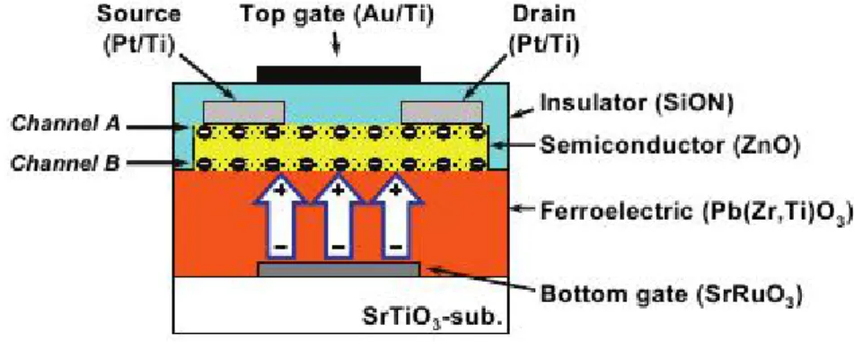
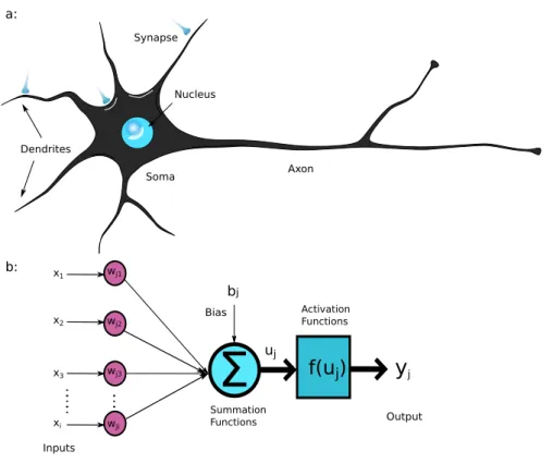
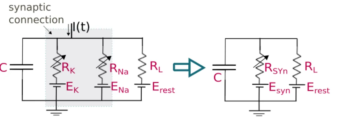
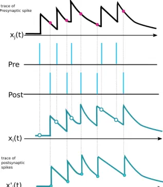
(10) Thèse de Mahyar Shahsavari, Lille 1, 2016. L IST OF F IGURES 2.4. 2.5. 2.6. 2.7. Spintronic memristor:Physical schematic of the circuit made of an interface between a semiconductor and a half-metal (ferromagnets with 100% spin-polarization at the Fermi level) (From [2]). . . . . . . . . . . . . . . . . . . . . . . . . . . . . . . . . . . . . . . . . . . . . Organic (polymeric) Memristor: the active channel is formed by PANI on top of a support and two electrodes. The region between PANI and PEO is called the ‘active zone’, and conductivity transformation is performed here. . . . . . . . . . . . . . . . . . . . . . . . . . . Physical structure of the NOMFET. It is composed of a p+ doped bottom-gate covered with silicon oxide. Source and drain electrodes are made of gold and Au NPs are deposed on the inter-electrode gap before the pentacene deposition. . . . . . . . . . . . . . . . . . . . . . . Ferroelectric Memristor, the OxiM transistor has dual channels at the upper and lower sides of the ZnO film, which are controlled independently by the top gate and the bottom gate, respectively. The bottom FET has the gate (SRO layer) and insulator (PZT ferroelectric layer) constituting a FeFET that has memory characteristics (from [3]). . . . . . . . . . . . . . . . . . . . . . . . . . . . . . . . . .. 2.8 Number of publications for each type of memristors. . . . . . . . . . . . . . . . . . . . . . . 2.9 Different memristor applications in different domains. . . . . . . . . . . . . . . . . . . . . . 2.10 Classification of domain studies using memristive devices . . . . . . . . . . . . . . . . . . . 3.1 3.2. Memristor-based IMP: a) circuit schematic, b) IMP truth table. . . . . . . . . . . . . . . . . . . . . NAND configuration with IMP: a) circuit schematic, b) required voltages for controlling the process, c) sequential truth table to obtain NAND. . . . . . . . . . . . . . . . . . . . . . . . . . . . . . . .. 23. 24. 24. 25 26 27 28 32 33 35 36. 3.3 3.4 3.5. Different states of a switch in a crossbar array. . . . . . . . . . . . . . . . . . . . . . . . . . . . . .. 3.6. Crossbar array architecture for exclusive-NOR function. . . . . . . . . . . . . . . . . . . . . . . .. 4.1. Computational architecture a) Von Neumman architecture, fast and costly memory are closer to cores in multiprocessor platforms as cashes and local memory as well as inexpensive and slower memory are in other layers close to magnetic memory to save the cost of CPU (memory hierarchy). b) Neuromorphic architecture inspired from neural networks in the biological brain, capable to conquer Von neumann bottelneck issue, performing parallel and cognitive computing, as well as considering that the synapses are local memories connected to each neurons as computational cores. 42. 4.2. Spike information coding strategies a)Rate coding, b)Latency coding, c)Phase coding, d)Rankcoding (spike-order coding), e)Population coding, f ) Sparse coding. . . . . . . . . . . . . . . . .. 4.3 4.4 4.5. Different states and configurations of the memristive switches in a crossbar array. . . . . . . . . . The crossbar array architecture for AND function with memristor switches: a) by applying the positive voltages all switches become open (clear), b) capture data in the input latches, c) transfer data to the wired-AND switches, d) if all inputs are ‘1’ (open) then the X spot is not negative so the output switch has enough voltage across it to be ON, e) open all wired-AND switches to be prepared to read output, f ) read output. . . . . . . . . . . . . . . . . . . . . . . . . . . . . . . . . . . . . .. two main topologies of artificial neural network architectures a)Feed-Forward Neural Networks (FFNN), b) Recurrent Neural Networks (RNN). . . . . . . . . . . . . . . . . . . . . . . . . . . . .. 36 38. 45. The structure of a neuron a)Physiological neuron, b) Artificial neuron model. . . . . . . . . . . .. 45 48. Electrical circuit represents Hodgkin-Haxley model of the neuron. a)Details circuit model of the neuron with sodium and potassium channels effects and leakage current, b) Equivalent circuit for more simplicity in solving equations. . . . . . . . . . . . . . . . . . . . . . . . . . . . . . . . . .. 49. 4.6. Simulation of a single LIF neuron in Matlab, the input spikes are applied in t=[10, 30, 40, 50] ms. Between 10 and 30 there is more decrease than between 30 and 40. . . . . . . . . . 4.7 Different Known types of neurons correspond to different values of the parameters a, b, c, and d could be reproduced by Izhikevich model From [4]. . . . . . . . . . . . . . . . . . . . 4.8 Different learning classifications. . . . . . . . . . . . . . . . . . . . . . . . . . . . . . . . . . . 4.9 Implementation of plasticity by local variables which each spike contributes to a trace x(t). The update of the trace depends on the sequence of presynaptic spikes . . . . . . . . . . . 4.10 Basic of spike-timing-dependent plasticity. The STDP function expresses the change of synaptic weight as a function of the relative timing of pre- and post-synaptic spikes. . . . .. 50 52 54 54 55. 4 © 2016 Tous droits réservés.. lilliad.univ-lille.fr.
(11) Thèse de Mahyar Shahsavari, Lille 1, 2016. List of Figures 4.11 Pair-based STDP using local variables. The spikes of presynaptic neuron j leave a trace x j (t ) and the spikes of the postsynaptic neuron i leave a trace x i (t ). The update of the weight W j i at the moment of a postsynaptic spike is proportional to the momentary value of the trace x j (t ) (filled circles). This gives the amount of potentiation due to pre-before-post pairings. Analogously, the update of W j i on the occurrence of a presynaptic spike is proportional to the momentary value of the trace x i (t ) (unfilled circles), which gives the amount of depression due to post-before-pre pairings . . . . . . . . . . . . . . . . . . . . . . . . . . . .. 57. 4.12 Triplet STDP model using local variables. The spikes of presynaptic neuron j contribute to a trace x j (t ), the spikes of postsynaptic neuron i contribute to a fast trace x i (t ) and a slow trace x i0 (t ). The update of the weight W j i at the arrival of a presynaptic spike is proportional value of the fast trace x i (t ) (green unfilled circles), as in the pair-based model. The update of the weight W j i at the arrival of a postsynaptic spike is proportional to the value of the trace x j (t ) (red filled circles) and the value of the slow trace x i0 (t ) just before the spike (green filled circles). . . . . . . . . . . . . . . . . . . . . . . . . . . . . . . . . . . . . . . . . . . . . . .. 58. 4.13 The suppression STDP model. A) Spike interactions in the suppression model, in which the impact of the presynaptic spike in a pair is suppressed by a previous presynaptic spike (top), and the impact of the postsynaptic spike is suppressed by a previous postsynaptic spike (bottom). B) Plasticity in the suppression model induced by triplets of spikes: pre-post-pre triplets induce potentiation (top left), and post-pre-post triplets induce depression (bottom right), From [5]. . . . . . . . . . . . . . . . . . . . . . . . . . . . . . . . . . . . . . . . . . . . . .. 59. 4.14 The NMDAR-based model. A) Schematic illustration of spike interactions in the NMDARbased model. The presynaptic spike up-regulates f rest, activates M dn and depresses the synapse. The postsynaptic spike down-regulates f r est , activates M up and potentiates the synapse. B) The effect is asymmetric, with pre-post-pre triplets inducing potentiation (top left) and post-pre-post depression (bottom right), From [5]. . . . . . . . . . . . . . . . . . .. 60. 4.15 Large scale spiking neural network systems, a) Principal architectural parts of a SpiNNaker processing node, b) In TrueNorth, conceptual blueprint of an architecture like the brain, tightly integrates memory, computation, and communication in distributed modules that operate in parallel and communicate via an event-driven platform. c) Schematic of HICANN board in BrainScales project, d) The chip comprises a 256 × 256 array of neuron elements, an asynchronous digital transmitter for sending the events generated by the neurons, a receiver block for accepting events from other sources, a router block for communicating packets among chips, and a memory blocks for supporting different network configurations. 63 5.1. N2S3 Logo . . . . . . . . . . . . . . . . . . . . . . . . . . . . . . . . . . . . . . . . . . . . . . . .. 68. 5.2. N2S3 Architecture. A network is organized in actors that may contain one or more network entities. Such entities could be for example, neurons, inputs or any other. . . . . . . . . . .. 70. 5.3. N2S3 Packages . . . . . . . . . . . . . . . . . . . . . . . . . . . . . . . . . . . . . . . . . . . . .. 71. 5.4. Heat map of the synaptic weights after learning the MNIST data base with 30 neurons on the output layer. . . . . . . . . . . . . . . . . . . . . . . . . . . . . . . . . . . . . . . . . . . . .. 73. 5.5. Input data for the freeway experiment comming from a spike-based camera. The spikes represent a variation of intensity for a given pixel and are generated asynchronously. . . .. 74. Heatmap showing the reconstruction of the contribution of each input pixel to the activity of the 10 output neurons for the freeway experiment. One can see that some neurons have clearly specialized to detect vehicles on a particular lane. . . . . . . . . . . . . . . . . . . . .. 74. a) Schematic of two simple biological neurons connected with synapse, b) Leaky Integrated & Fire model of neuron connected with artificial synapse (memristor) . . . . . . . . . . . .. 79. Memorization inspired from biology, the data is stored in Long-Term Memory (LTM) if the spikes are repeated in a certain time-window, otherwise Short-Term Memory (STM) will store temporary data. . . . . . . . . . . . . . . . . . . . . . . . . . . . . . . . . . . . . . . . . .. 79. 5.6. 6.1 6.2. 5 © 2016 Tous droits réservés.. lilliad.univ-lille.fr.
(12) Thèse de Mahyar Shahsavari, Lille 1, 2016. L IST OF F IGURES 6.3 6.4. 6.5. Artificial synapse: a) Schematic view of the NOMFET as a volatile memory, b) TiO2 based nonvolatile memory, c) Synapse box schematic, d) Equivalent circuit with simple elements 81 Synaptic weights (conductance of non volatile memristor) learned in simulation using the synapse box with 100 output neurons. The weights in the corners are random because they were always filtered out by the volatile memristor and thus are never modified or even read. 82 Recognition rate as a function of number of output neurons. In the box plot for each number of neuron, we compare the recognition rate of the two synapse models. The whiskers of the box plot represent the minimum and maximum recognition rates of the 10 simulations. . 83. Neuromorphic vs SNN, a) The memristive synapse connects the spiking neurons in configurable crossbar array suitable for stdp unsupervised learning, the presynaptic neurons are considered as inputs and postsynaptic neurons play output rolls. b) The spiking neural network two layers of this three layers could similarly operates as crossbar array. . . . . . 7.2 Sample heat maps of the synaptic weights after network training with four different numbers of output neurons (20, 30, 50 and 100). . . . . . . . . . . . . . . . . . . . . . . . . . . . . . . 7.3 The comparison of three different distributions for generating spike train by transferring MNIST database pixels to spike train. These distributions are tested with different number of neurons=20, 30, 50, 100. . . . . . . . . . . . . . . . . . . . . . . . . . . . . . . . . . . . . . . 7.4 The recognition rate of the network using different number of neurons and three spike train distributions. . . . . . . . . . . . . . . . . . . . . . . . . . . . . . . . . . . . . . . . . . . . . . . 7.5 The comparison of different STDP-window duration for using different number of neurons=20, 30, 50, 100. The MNIST digits dataset after converting to the corresponding spikes to the pixels densities, are presenting to the network for 350 ms for (each frame). The 150 ms pause between each digit presenting are considered. This figure illustrates the performance of neural network using four various number of neurons and different STDP-windows. . . 7.6 The recognition rate of the network using different number of neuron and six different STDP-wnidows. . . . . . . . . . . . . . . . . . . . . . . . . . . . . . . . . . . . . . . . . . . . . 7.7 The comparison of various threshold (15, 25, 35, 45 mV) for using different number of neurons=20, 30, 50, 100. The threshold between 25 and 35 mV demonstrate better performance in the network, however, in the network with smaller number of neurons the neuron with less threshold have still acceptable performance and on the contrary in larger neural networks the neuron with more firing threshold voltage (such as 45 mV using for the 100 output neurons) have demonstrated acceptable performance too. . . . . . . . . . . . . . . 7.8 comparing network performance using various number of neuron with different threshold 7.9 The comparison of various fitting parameters (β) for using different number of neurons=20, 30, 50, 100. The results demonstrate better performance using β between 1.8 and 2. However, the differences are not distinguishable which is a prove of memristor devices robustness to the variations. . . . . . . . . . . . . . . . . . . . . . . . . . . . . . . . . . . . . . . . . . 7.10 comparing network performance using various number of neurons with different fitting parameter (β) for synapse model. . . . . . . . . . . . . . . . . . . . . . . . . . . . . . . . . . . 7.11 Using the best parameters significantly improves the recognition rate. . . . . . . . . . . . . 7.1. 8.1 8.2 8.3 8.4 8.5 8.6 8.7 8.8. Restricted Boltzmann Machine is a network of neurons which neurons in one layer are connected to all neurons in the next layer. . . . . . . . . . . . . . . . . . . . . . . . . . . . . . Siegert abstract neuron model [6] . . . . . . . . . . . . . . . . . . . . . . . . . . . . . . . . . . Stacking RBMs as the main building blocks of DBN . . . . . . . . . . . . . . . . . . . . . . . Some sample images from ORL dataset . . . . . . . . . . . . . . . . . . . . . . . . . . . . . . The proposed DBN with Siegert neurons for learning ORL . . . . . . . . . . . . . . . . . . . Visualizing the learned features by hidden units . . . . . . . . . . . . . . . . . . . . . . . . . Accuracy of the proposed DBN with Siegert neurons in face recognition on ORL dataset . Decreasing the number of epochs and increasing the mini-batch size can reduce the model accuracy . . . . . . . . . . . . . . . . . . . . . . . . . . . . . . . . . . . . . . . . . . . . . . . .. 86 87. 88 90. 91 92. 93 93. 94 95 95. 98 100 101 101 102 102 103 103. 6 © 2016 Tous droits réservés.. lilliad.univ-lille.fr.
(13) Thèse de Mahyar Shahsavari, Lille 1, 2016. 8.9. The upper row shows 10 of the training images and the lower one illustrate the corresponding reconstructed images . . . . . . . . . . . . . . . . . . . . . . . . . . . . . . . . . . . . . . . 104 8.10 The upper row shows 10 of the test images and the lower one illustrate the predicted images 104. List of Tables 2.1. Table of different class of memristors based on different materials and its applications, the first university/lab announcement of the device is listed too. . . . . . . . . . . . . . . . . . .. 26. 3.1 3.2. Different logic operations made by IMP operations and the number of required memristors . . . . The number of memristive switches to make logic gates for the imp and crossbar array approaches.. 34 38. 6.1. Comparing network architecture efficiency for two synapses: nonvolatile (NV) v.s volatilenonvolatile (VNV) synapse . . . . . . . . . . . . . . . . . . . . . . . . . . . . . . . . . . . . . .. 83. 7.1. Best parameters vs. baseline parameters . . . . . . . . . . . . . . . . . . . . . . . . . . . . . .. 94. 8.1. LIF parameters . . . . . . . . . . . . . . . . . . . . . . . . . . . . . . . . . . . . . . . . . . . . . 101. 7 © 2016 Tous droits réservés.. lilliad.univ-lille.fr.
(14) Thèse de Mahyar Shahsavari, Lille 1, 2016. © 2016 Tous droits réservés.. lilliad.univ-lille.fr.
(15) Thèse de Mahyar Shahsavari, Lille 1, 2016. Chapter. 1. Introduction 1.1. Introduction. The two most important demands of humans using ICT devices and technologies are becoming two hottest topic of research in computer science and engineering namely Big Data and Internet of Things (IoT). In both domains, the way of processing data is quite important. In Big Data the clustering, classification, and prediction are not avoidable to use and process the data efficiently. In IoT, the smart devices are connected to other smart devices using different sensors. Machine learning recently proposed promising solution for processing data in these two domains. By 2020, there will be 50 to 100 billion devices connected to the Internet, ranging from smartphones, PCs, and ATMs (Automated Teller Machine) to manufacturing equipment in factories and products in shipping containers [7]. For the Big Data or sensory data not only an efficient processing algorithm is necessary but also finding a new fast, parallel and power-efficient hardware architecture is unavoidable. Machine learning algorithms are widely used for data classification in software domain and using conventional hardware platform. These algorithms on nowadays computers consume a remarkable time and energy. The reason is that in conventional computing, the way of communicating between memory and central processing unit (CPU) is not efficient. The memory wall or Von Neumann memory bottelneck is the growing disharmony of communication speed between the CPU and memory outside the CPU chip. An important reason for this disharmony is the restricted communication bandwidth beyond chip boundaries, which is referred to as bandwidth wall as well. The CPUs access both data and program in memory using the same shared resources. Finally, CPUs spend most of their time idle. Using emerging technologies such as memristors [1], there is possibility of performing both information processing and storing the computational results on the same physical platform [8]. Memristors have the potential to be a promising device for novel paradigms of computation as well as new generation of memory. The characteristics of memristor are promising to design a processing unit with local access memory rather than non-local and shared memory. The new high performance architecture for next generation of computation regarding to emerging technologies could be in logic or analog domain. Memristors have potential for both digital and analog paradigms of computations. Another novel alternative architecture suitable for neural network and machine learning algorithms is proposed as Spiking Neural Network (SNN) system which is known as Neuromorphic architecture too. SNN is the known way to realize the neural network software abilities on a hardware architecture. The mammalian nervous system is a network of extreme complexity which is able to perform cognitive computation in a parallel and power-efficient manner. Understanding the principles of brain processing for computational modeling is one of the biggest challenges of the 21st century that led to the new branch of research e.g., neuromorphic computing. Neuromorphic engineering represents one of the promising fields for developing new computing paradigms complementing or even replacing current Von Neumann architecture [9]. The requirements for implementing a SNN architecture (neuromorphic) are providing electronic devices that can mimic the biological neural network components such as neurons and synapses. The Spiking neural model is an electrical model of physiological neuron 9 © 2016 Tous droits réservés.. lilliad.univ-lille.fr.
(16) Thèse de Mahyar Shahsavari, Lille 1, 2016 CH 1.. I NTRODUCTION that has been implemented on the circuit using state-of-the-art technologies e.g., CMOS transistors or on low-power CMOS design using subthreshold regime transistor [10]. The synapse in biological neural network reacts as a plastic connection controller between two neurons. Recently, emerging devices in nano-scale have demonstrated novel properties for making new memories and Artificial synapse. One of those is the memristor that was hypothetically presented by Leon Chua in 1971 [11] and after a few decades, HP was the first to announce the successful memristor fabrication [1]. The unique properties in memristor nano-devices such as, extreme scalability, flexibility because of analog behavior, and ability to remember the last state make the memristor a very promising candidate to apply it as a synapse in Spiking Neural Network (SNN) [12].. 1.2. Part I:Motivation, state-of-the-art and application of using emerging nanodevices for unconventional computing. The first part of this dissertation contains the mathematic and physical model of memristor, memristive nanodevice technologies, as well as different applications of this emerging technology. Memristor can remember its last state after the last power plugging and has a simple physical structure, highdensity integration, and low-power consumption. These features make the memristor an attractive candidate for building the next generation of memories [13–15], an artificial synapse in Spiking Neural Network architectures [12, 16], and as a switch in crossbar array configurations [17]. Different device structures are still being developed to determine which memristor device can be presented as the best choice for commercial use in memory/flash manufacturing or in neuromorphic platforms. This is based on different factors such as size, switching speed, power consumption, switching longevity, and CMOS compatibility. A comprehensive survey particularly on recent research results and recent development of memristive devices seems be quite useful for future research work and developments. To better understanding how memristor can restore the data and how it could be flexible to modify the conductances to be replaced as a synapse, we have modeled the behavior of this device. In addition, we perform a classification of the devices based on the manufacturing technology. In this classification, we discuss different characteristics of various devices. We study the potential applications of a memristor built using specific technology. The advantages and disadvantages of each class of memristor with various type of device materials are discussed. Furthermore, we discuss potential applications of memristor nanodevice in nonvolatile memories such as RRAM, PCM, CBRAM, FeRAM and MRAM, digital computation, analog and neuromorphic domains. In the second chapter, we discuss two methods for unconventional digital computing by memristive two-terminal devices [18]. Two main digital computation approaches, namely material implication (IMP) or stateful logic [19, 20] and programmable crossbar architecture [21, 22] are studied in this chapter. By applying memristor as a digital switch, a high memristance (memristor resistance) is considered as logic ‘0’ and a low memristance is considered as logic ‘1’. First and foremost, based on the previous research works on IMP, we establish a functionally complete Boolean operation to be able to build all standard logic gates. Subsequently, building the digital gates has been performed using programmable crossbar architectures. Programmable crossbar architectures have been proposed as a promising approach for future computing architectures because of their simplicity of fabrication and high density, which support defect tolerance. At the end of Chapter 3, the comparison of two methods in digital computation is presented. In the last chapter of part I, the basic definition of neuromorphic or Spiking Neural Network (SNN) architecture have been introduced. Neuromorphic computing has the potential to bring very low power computation to future computer architectures and embedded systems [23]. The main remarkable difference between conventional Von Neumann architecture and neuromorphic systems is in their use of memory structures. The way of communication between memory and central processing unit (CPU) in conventional computing is not very efficient which is known as Von Neumann memory bottelneck. CPUs spend most of their time idle because the speed difference between the CPU and memory. The solution that has been applied in Von Neumann architecture is memory 10 © 2016 Tous droits réservés.. lilliad.univ-lille.fr.
(17) Thèse de Mahyar Shahsavari, Lille 1, 2016. Part II:Our contribution in spiking neural network architecture: Simulator, New synapse box, Parameter exploration and Spiking deep learning hierarchy. In other words, a limited amount of fast but costly memory sit closer to the processing unit, while most of the data is stored in a cheaper but larger memory. By proposing computing unit next to the local memory, neuromorphic brain-inspired computing paradigms offer an attractive solution for implementing alternative non von Neumann architectures, using advanced and emerging technologies [9,24]. Artificial neural network (ANN) is a mathematical model of the network of neurons in mammalian brain though SNN is an electronic hardware neuromorphic model of biological brain. SNNs provide powerful tools to emulate data processing in the brain, including neural information processing, plasticity and learning. Consequently, spiking networks offer solutions to a broad range of specific problems in applied engineering image detection, event detection, classification, speech recognition and many cognitive computation domain applications. Neurons communicate together using spikes. In Chapter 4, we review different ways of coding data to spikes known as spike information coding methods. Furthermore, we study the network topologies and configurations. The interconnection among units can be structured in numerous ways resulting in numerous possible topologies. Two basic classes are defined: Feed-Forward Neural Networks (FFNN) and Recurrent (or feedback) Neural Networks (RNN) depicted in Figure 4.3. We add a discussion in more modern neural networks such as Convolutional Neural Networks (CNN) [25], and Deep Belief Networks (DBNs) [26]. Moreover, various spiking model of neurons as dynamic elements and processing units are reviewed. We discuss which model we have used in our platform and why we choose this model. Thanks to the plasticity property of synapse, in neural network system, we can basically say the synapse is where the learning happens. Therefore, in this chapter both synapse and learning are studied. Additionally, we discussed various classes of learning algorithms as well as a comprehensive study of Spike-Timing Dependent Plasticity (STDP) [27, 28] is presented. This comprehensive study includes presenting different models for STDP learning based on single or multiple pre- or postsynaptic spikes occurring across a synapse in an interval of time. Finally in Chapter 4, we applied lateral inhibition which is winner-take-all (WTA) [29, 30] in our platform as well as homeostasis as a method of neuron adaptation of learning.. 1.3. Part II:Our contribution in spiking neural network architecture: Simulator, New synapse box, Parameter exploration and Spiking deep learning. The second part of the thesis consists of our contributions to neuromorphic computing and SNN architecture. In Chapter 5, we present and develop N2S3 (for Neural Network Scalable Spiking Simulator), an open-source event-driven simulator that is built to help design spiking neuromorphic circuits based on nanoelectronics. It is dedicated to intermediate modeling level, between low-level hardware description languages and high-level neural network simulators used primarily in neurosciences as well as the integration of synaptic memristive device modeling, hardware constraints and any custom features required for the target application. N2S3 has been developed from the ground up for extensibility, allowing to model various kinds of neurons and synapses, network topologies, learning procedures, reporting facilities, and to be user-friendly, with a domain specific language to easily express and run new experiments. For experimental set up, N2S3 is distributed with the implementation of two “classical” experiments: handwritten digit recognition on the MNIST dataset [25, 31] and the highway vehicle counting experiment [32]. In Chapter 6, with the combination of a volatile and a nonvolatile memristor we introduce and design a new artificial synapse box that can improve learning in spiking neural networks architectures [33]. This novel synapse box is able to forget and remember by inspiration from biological synapses. The nonvolatility is a unique property in memristor nanodevice to introduce it as a promising candidate in building next generation of non-volatile memory. However, by inspiring of physiological synapse, a synapse that can forget unimportant data (non-frequent spikes) and remember significant data (frequent spike trains) can support network to improve learning process. 11 © 2016 Tous droits réservés.. lilliad.univ-lille.fr.
(18) Thèse de Mahyar Shahsavari, Lille 1, 2016 CH 1.. I NTRODUCTION Thanks to close collaboration with the nano-electronics research center in the University of Lille (IEMN), we have had the opportunity of studying the suitability of different types of memristors (TiO2 , NOMFET, magnetoresistive, magnetoelectric) to build a spiking neural network hardware platform. To add the forgetting property to the synapse box, we have used a volatile memristor named NOMFET (Nanoparticle Organic Memory Field-Effect Transistor). We have merged NOMFET with a nonvolatile solid-state meristor nanodevice. At the end of this chapter, we evaluate the synapse box proposal by comparing it with a single non-volatile memory synapse by simulation on the MNIST handwritten digit recognition benchmark. Specific application domains such as Big Data classification, visual processing, pattern recognition and in general sensory input data, require information processing systems which are able to classify the data and to learn from the patterns in the data. Such systems should be power-efficient. Thus researchers have developed brain- inspired architectures such as spiking neural networks. In Chapter 7, we surveyed brain- inspired architectures approaches with studying well-known project and architecture in this neuromorphic domain. For large scale brain-like computing on neuromorphic hardware we have recognized four approaches: • Microprocessor based approaches where the system can read the codes to execute and model the behavior of neural systems and cognitive computation such as the SpiNNaker machine [34]. • Fully digital custom circuits where the neural system components are modeled in circuit using sate-of-the-art CMOS technology e.g., IBM TrueNorth machine [23]. • Analog/digital mixed-signal systems that model the behavior of biological neural systems, e.g. the NeuroGrid [35] and BrainScales [36] projects. • Memristor crossbar array based systems where the analog behavior of the memristors emulate the synapses of a spiking neural network [37]. We have studied large scale brain-like architectures such as SpiNNaker, IBM TrueNorth, NeuroGrid, and BrainScales to recognize the cons and pros of these projects to have our optimized evaluation and exploration of required items and parameters for neuromorphic and brain-like computation platforms. Spiking neural networks are widely used in the community of computational neuroscience and neuromorphic computation, there is still a need for research on the methods to choose the optimum parameters for better recognition efficiency. Our main contribution in Chapter 7 is to evaluate and explore the impact of several parameters on the learning performance of SNNs for the MNIST benchmark: the number of neurons in the output layer, the duration of the STDP window, various thresholds for adaptive threshold neurons, different distributions of spikes to code the input images and the memristive synapse fitting parameter. This evaluation has shown that a careful choice of a few parameters can significantly improve the recognition rate on this benchmark. Deep learning is currently a very active research area in machine learning and pattern recognition society due to its potential to classify and predict as a result of processing Big data and Internet of Things (IoT) related data. Deep Learning is a set of powerful machine learning methods for training deep architectures. Considering the inherent inefficiency of learning methods from traditional Artificial Neural Networks in deep architectures, Contrastive Divergence (CD) has been proposed to train Restricted Boltzmann Machines (RBM) as the main building blocks of deep networks [38]. In Chapter 8 deep learning architectures are introduced in SNN systems. In SNN, neurons communicate using spikes [39]. Therefore, we have to design an architecture of neurons that are able to implement spiking data. Consequently, we present a framework for using Contrastive Divergence to train an SNN using RBM and spiking neurons. The obtained recognition rate or network accuracy of the architecture using CD algorithms for learning was 92.4%. This framework can open a new window toward the neruromorphic architecture designer to apply the state-of-the-art of machine learning learning algorithm in SNN architecture.. 12 © 2016 Tous droits réservés.. lilliad.univ-lille.fr.
(19) Thèse de Mahyar Shahsavari, Lille 1, 2016. Manuscript outline. CH1. Introduction Part I. Using nanodvices for unconventional computing. Part II. Our contribution in spiking neural network architecture. Ch2. Memristor new emerging device:review and applications. Ch5. N2S3, scalable neuromorphic hardware simulator. Ch3. Unconventional digital computing using memristors. Ch6. Combining a Volatile and Nonvolatile Memristor in synapse box. Ch4. Neuromorphic computing in Spiking Neural Network Architecture. Ch7. Evaluation and parameter exploration in SNN. Ch8. Deep learning in spiking neural network Figure 1.1: General overview of the manuscript.. 1.4. Manuscript outline. This manuscript presents a spiking neural network platform suitable to hardware implementation with a focus on learning in SNN. Therefore in the first two chapters, we review cons and pros of memristor and memristive-based computation. The different models and technologies of memristor beside the applications is presented in chapter 2. The third chapter consists of using memristors in the unconventional digital manner. In the chapter 4, the principals of neuromorphic and spiking neural network architecture is described. Our contribution in designing and presenting spiking neural network architecture is presented in the second part of this manuscript. First of all, in the contribution part we present our neuromorphic hardware simulator. Second, we propose an artificial synapse box to improve learning by combining volatile and nonvolatile types of memristor devices. Furthermore, in Chapter 7, we discuss different parameters in SNN architecture and evaluate the effect of each parameters in learning. In Chapter 8, deep learning in spiking neural network is presented. Finally the conclusion and potential future work are explained. A general overview of this dissertation is shown in Figure 1.1.. 13 © 2016 Tous droits réservés.. lilliad.univ-lille.fr.
(20) Thèse de Mahyar Shahsavari, Lille 1, 2016. © 2016 Tous droits réservés.. lilliad.univ-lille.fr.
(21) Thèse de Mahyar Shahsavari, Lille 1, 2016. Part I. Motivation, state-of-the-art and application of using emerging nanodevices for unconventional computing. 15 © 2016 Tous droits réservés.. lilliad.univ-lille.fr.
(22) Thèse de Mahyar Shahsavari, Lille 1, 2016. © 2016 Tous droits réservés.. lilliad.univ-lille.fr.
(23) Thèse de Mahyar Shahsavari, Lille 1, 2016. Chapter. 2. Memristor nanodevice for unconventional computing: review and applications Abstract. A memristor is a two-terminal nanodevice. Its properties attract a wide community of researchers from various domains such as physics, chemistry, electronics, computer and neuroscience. The simple structure for manufacturing, small scalability, nonvolatility and potential of using in low power platforms are outstanding characteristics of this emerging technology. In this chapter, we review a brief literature of memristor from mathematic model to the physical realization and different applications. We discuss different classes of memristors based on the material used for its manufacturing. The potential applications of memristor are presented and a wide domain of applications are classified.. 2.1. Introduction. Memristor has recently drawn the wide attention of scientists and researchers due to non-volatility, better alignment, and excellent scalability properties [40]. Memristor has initiated a novel research direction for the advancement of neuromorphic and neuro-inspired computing. Memristor remembers its last state after the last power plugging and has a simple physical structure, high-density integration, and low-power consumption. These features make the memristor an attractive candidate for building the next generation of memories [13]. In addition, from high-performance computing point of view, the memristor has the potential capability to conquer the memory bottleneck issue, by utilizing computational unit next to the memory [8]. Due to these unique properties and potentials of the memristor, neuroscientists and neuromorphic researchers apply it as an artificial synapse in Spiking Neural Network (SNN) architectures [12]. Memristor was predicted in 1971 by Leon Chua, a professor of electrical engineering at the University of California, Berkeley, as the fourth fundamental device [11]. Publishing a paper in the Nature journal by Hewlett Packard (HP) [1] in May 2008, announced the first ever experimental realization of the memristor, caused an extraordinary increased interest in this passive element. Based on the symmetry of the equations that govern the resistor, capacitor, and inductor, Chua hypothesized that fourth device should exist that holds a relationship between magnetic flux and charge. After the physical discovery of the memristor, several institutions have published the memristor device fabrications using a variety of different materials and device structures [1, 2, 41–43]. In 2009, Biolek et al. modeled nonlinear dopant drift memristor by SPICE [44]. One year later, Wei Lu, professor at the University of Michigan proposed a nanoscale memristor device which can mimic 17 © 2016 Tous droits réservés.. lilliad.univ-lille.fr.
(24) Thèse de Mahyar Shahsavari, Lille 1, 2016 CH 2.. M EMRISTOR NANODEVICE FOR UNCONVENTIONAL COMPUTING :. REVIEW AND APPLICATIONS. the synapse behavior in neuromorphic systems [45]. Later on, in 2011 a team of multidisciplinary researchers from Harvard University published an interesting paper on programmable nanowire circuits for using in nanoprocessors [46]. Until June 2016, based on the Scopus bibliographic database, 2466 papers have been published in peer-reviewed journals and ISI articles which are related to memristor fabrication or applications of the memristor in different science and technology domains. Memristors are promising devices for a wide range of potential applications from digital memory, logic/analog circuits, and bio-inspired applications [16]. Especially because the nonvolatility property in many types of memristors,they could be a suitable candidate for making non-volatile memories with ultra large capacity [14]. In addition to non-volatility, the memristor has other attractive features such as simple physical structure, high-density, low-power, and unlimited endurance which make this device a proper choice for many applications. Different device structures are still being developed to determine which memristor device can be presented as the best choice for commercial use in memory/flash manufacturing or in neuromorphic platforms. This is based on different factors such as size, switching speed, power consumption, switching longevity, and CMOS compatibility. The rest of the chapter is organized as follows: In Section 2, a general overview of the memristor is done and the electrical properties have been investigated. Section 3 presents memristor implementation and fabrication. We investigate various types of memristors based on the different materials that have been used in the fabrication. In Section 4, potential applications of Memristor has been studied. Section 5 deals with streams of research, we have investigated a research classification from the physics level to the system design. Finally, we describe a brief summary and the future work.. 2.2. Memristor device overview and properties. In this section, we discuss the memristor nanodevice which is believed to be the fourth missing fundamental circuit element, that comes in the form of a passive two-terminal device. We discuss how it can remember its state, and what is its electrical model and particular properties.. 2.2.1. Memristor a missing electrical passive element. Memristor is a contraction of “memory & resistor,” because the basic functionality of the memristor is to remember its state history. This characteristic proposes a promising component for next generation memory. Memristor is a thin-film electrical circuit element that changes its resistance depending on the total amount of charge that flows through the device. Chua proved that memristor behavior could not be duplicated by any circuit built using only the other three basic electronic elements (Resistor,Capacitor, Inductor), that is why the memristor is truly fundamental. As it is depicted in Figure 2.1, the resistor is constant factor between the voltage and current (d v = R.d i ), the capacitor is a constant factor between the charge and voltage (d q = C .d v), and the inductor is a constant factor between the flux and current (d ϕ = L.d i ). The relation between flux and charge is Obviously missing (d ϕ = M .d q) that can be interpreted by a fourth fundamental element such as memristor [11]. Obviously, in memristive devices, the nonlinear resistance can be changed and memorized by controlling the flow of the electrical charge or the magnetic flux. This control any two-terminal black box is called a memristor if, and only if, it exhibits a pinched hysteresis loop for all bipolar periodic input current signaling is interesting for the computation capability of a device similar to the controlling of the states of a transistor. For instance in an analog domain, one can control the state of a transistor to stay in an active area for amplification. Nevertheless, in the digital domain to stay in Off (cut-off) state for logic ’0’ and in On (saturated) state for logic ’1’ one can perform with controlling the gate voltage. The output current in MOSFET (Metal-Oxide semiconductor Field Effect Transistor) is managed by changing the gate voltage as well as in BJT (Bipolar Junction Transistor) the input current (base current) can control the output current (collector-emitter current). The main difference between the memristor and transistor for managing the states is that in transistor there is a third terminal to control the states however, in contrast a memristor is a two-terminal device and there is no extra terminal to control the device state. The challenge of using memristor as a computational component 18 © 2016 Tous droits réservés.. lilliad.univ-lille.fr.
(25) Thèse de Mahyar Shahsavari, Lille 1, 2016. Memristor device overview and properties. Figure 2.1: Relations between the passive devices and the anticipating the place of the fourth fundamental element based on the relations between charge (q) and flux (ϕ) (from [1]).. instead of transistor lies in the ability to control the working states as accurate as possible. Indeed, in a memristor both potentials for analog and digital computing have been presented. Consequently, using memristor in digital computing to make gate library or crossbar architecture as well as using memristor in analog domain (neuro-inspired or traditional) for computation are introduced in several work [8, 19–21, 47]. In next sections, we discuss different possibilities and our contributions to apply memristor in both digital and analog platforms.. 2.2.2. Memristive device functionality. When you turn off the voltage, the memristor remembers its most recent resistance until the next time you turn it on, whether that happens a day later or a year later. It is worth mentioning that the duration to store the data in resistive form is dependent of the nano-device material. In other words, the volatility is different depending on the device materials in fabrication. To understand the functionality of a memristor, let us imagine a resistor as a pipe which water flows through it. The water simulates the electric charge. The resistor obstruction of the flow of charge is comparable to the diameter of the pipe: the narrower the pipe, the greater the resistance. For the history of circuit design, resistors have had a fixed pipe diameter. But a memristor is a pipe that its diameter changes with the amount and direction of the water flows through it. If water flows through this pipe in one direction, it expands the pipe diameter (more conductive). But if the water flows in the opposite direction and the pipe shrinks (less conductive). Furthermore, let us imagine while we turn off the flow, the diameter of the pipe freezes until the water is turned back on. It mimics the memristor characteristic to remember last state. This freezing property suits memristors brilliantly for the new generation of memory. The ability to indefinitely store resistance values means that a memristor can be used as a nonvolatile memory. Chua demonstrated mathematically that his hypothetical device would provide a relationship between flux and charge similar to what a resistor provides between voltage and current. There was no obvious physical interaction between charge and the integral over the voltage before HP discovery. Stanley Williams in [48] explained how they found the missing memristor and what is the relation between what they found and Chua mathematic model. In Figure 2.2, the oxygen deficiencies in the TiO2−x manifest as bubbles of oxygen vacancies scattered throughout the upper layer. A positive voltage on the switch repels the (positive) oxygen deficiencies in the metallic upper TiO2−x layer, sending them into the insulating TiO2 layer below. That causes the boundary between the two materials to move down, increasing the percentage of conducting TiO2−x and thus the conductivity of the entire switch. 19 © 2016 Tous droits réservés.. lilliad.univ-lille.fr.
(26) Thèse de Mahyar Shahsavari, Lille 1, 2016 CH 2.. M EMRISTOR NANODEVICE FOR UNCONVENTIONAL COMPUTING :. REVIEW AND APPLICATIONS. Therefore, the more positive voltage causes the more conductivity in the cube. A negative voltage on. Figure 2.2: A material model of the memristor schematic to demonstrate TiO2 memristor functionality, positive charge makes the device more conductive and negative charge makes it less conductive. the switch attracts the positively charged oxygen bubbles, pulling them out of the TiO2 . The amount of insulating of resistive TiO2 increases, thereby making the switch more resistive. The more negative voltage causes the less conductivity in the cube. What makes this switch a special device? When the voltage across the device is turned off–positive or negative–the oxygen bubbles do not migrate. They will freeze where they have been before, which means that the boundary between the two titanium dioxide layers is frozen. That is how the Memristor “remembers” the last state of conductivity as well as it proves the plasticity properties in memristor to be applied as a synapse in an artificial neural network architecture and neuromorphic platform.. 2.2.3. Electrical model. When an electric field is applied to the terminals of the memristor, the shifting in the boundary between its doped and undoped regions leads to variable total resistance of the device. In Figure 2.3.a, the electrical behavior of memristor can be modeled as follows [1]: v(t ) = R mem i (t ). R mem = RON. w(t ) w(t ) + ROF F (1 − ) D D. (2.1). (2.2). where w(t ) is the width of the doped region, D is the overall thickness of the TiO2 bi-layer, RON is the resistance when the active region is completely doped (w = D) and ROF F is the resistance, when the TiO2 bi-layer is mostly undopped (w→ 0). d w(t ) RON = µv i (t ) dt D. (2.3). which yields the following formula for w(t ): w(t ) = µv. RON q(t ) D. (2.4). Where µv is the average dopant mobility. By inserting Equation (2.4) into Equation (2.2) and then into Equation (2.1) we obtain the memristance of the device, which for RON «ROF F simplifies to: R mem = M (q) = ROF F (1 −. µv RON q(t )) D2. (2.5). 20 © 2016 Tous droits réservés.. lilliad.univ-lille.fr.
(27) Thèse de Mahyar Shahsavari, Lille 1, 2016. Memristor classification based on different materials and applications W(t). a. Pt. Doped. Undoped. Pt. D. b. Figure 2.3: Memristor schematic and behavior: a) the memristor structure, the difference in applied voltage changes doped and undoped regions, b) current versus voltage diagram, which demonstrates hysteresis characteristic of a memristor, in the simulation we apply the sinusoidal input wave with an amplitude of 1.5v, different frequencies, RON = 100Ω, ROF F = 15kΩ, D = 10nm, µv = 10−10 cm 2 s −1 V −1 .. Equation (2.5) shows the dopant drift mobility µv and semiconductor film thicknesses D are two factors with crucial contributions to the memristance magnitude. Subsequently, we can write Kirchoff’s voltage law for memristor given by: v(t ) = M (q)i (t ) (2.6) By using Verilog-A HDL, we simulate the behavior of memristor, based on its behavioral equations. To investigate the characteristics of memristor in electrical circuits, the Verilog-A model of memristor behavior must be applied as a circuit element in the HSPICE netlist. In the HSPICE circuit, we apply a sinusoidal source to observe the memristor reaction in a simple circuit consisting of the memristor and the sinusoidal source. Figure 2.3.b depicts i − v plot of memristor terminals that we measured in our simulation. This i − v plot, which is the most significant feature of memristor [49], is namely called “pinched hysteresis loop”. The i − v characteristic demonstrates that memristor can “remember” the last electric charge flowing through it by changing its memristance. Therefore, we can use the memristor as a latch to save the data and also as a switch for computing. Moreover, in Figure 2.3.b, it is depicted that the pinched hysteresis loop is shrunk by increasing frequency. In fact, when the frequency increases toward infinity, memristor behavior is similar to a linear resistor.. 2.3. Memristor classification based on different materials and applications. A memristor is generally made from a metal-insulator-metal (MIM) sandwich with the insulator usually consisting of a thin film like TiO2 and a metal electrode like Pt. A memristor can be made from any Metal Insulator Metal (MIM) sandwich which exhibits a bipolar switching characteristic. It means that TiO2 and Pt are not the only materials to fit the criteria for a memristor. For instance, Wan Gee Kim et al. [50] conducted a systematic approach using the HfO2 and ZrO2 as substitutes for TiO2 , also using TiN or Ti/TiN electrode instead of Pt. Basically, any two-terminal black box is called a memristor only if it can present a pinched hysteresis loop for all bipolar periodic input signals. Following we discuss four most significant materials for memristor fabrication namely: • Resistive memristor • Spintronic memristor 21 © 2016 Tous droits réservés.. lilliad.univ-lille.fr.
(28) Thèse de Mahyar Shahsavari, Lille 1, 2016 CH 2.. M EMRISTOR NANODEVICE FOR UNCONVENTIONAL COMPUTING :. REVIEW AND APPLICATIONS. • Organic (Polymeric) memristor • Ferroelectric memristor. 2.3.1. Resistive Memristor. Before the memristor getting well-known, resistive materials have already been widely used in the resistive random access memories (ReRAM/RRAM) [51]. The storage function of ReRAM is realized by an intrinsic physical behavior in ReRAM, that is called resistive switching. The resistive material can be switched between a high resistance state (HRS) and a low resistance state (LRS) under an external electrical input signal. The TiO2 memristor is a ReRAM fabricated in nanometre scale (2-3 nm) thin film that is depicted in Figure 2.3.a , containing a doped region and an undoped region. Strukov et al. [1] exploit a very thin-film TiO2 sandwiched between two platinum (Pt) contacts and one side of the TiO2 is doped with oxygen vacancies, which are positively charged ions. Therefore, there is a TiO2 junction where one side is doped and the other is undoped. Such a doping process results in two different resistances: one is a high resistance (undoped) and the other is a low resistance (doped). The application of an external bias v(t) across the device will move the boundary between the two regions by causing the charged dopants to drift. How TiO2 could change and store the state has been introduced in 2.2.2. The obvious disadvantage of the first published TiO2 memristor was its switching speed (operate at only 1Hz). The switching speed was not comparable with SRAM, DRAM and even flash memory. Flash exhibit writing times of the order of a microsecond and volatile memories have writing speeds of the order of hundreds of picoseconds. Many research groups in different labs published their fabrication results to demonstrate a faster switching speed device. In October 2011, HP lab developed a memristor switch using a SET pulse with a duration of 105 ps and a RESET pulse with a duration of 120 ps. The associated energies for ON and OFF switching were computed to be 1.9 and 5.8 pJ, respectively which are quite efficient for power-aware computations. The full-length D (Figure 2.3.a) of the TiO2 memristor is 10 nm [52] that proposes high-density devices in a small area in VLSI. A research team at the University of Michigan led by Wei Lu [45] demonstrated another type of resistive memristor that can be used to build brain- like computers and known as amorphous silicon memristor. The Amorphous silicon memristor consists of a layered device structure including a cosputtered Ag and Si active layer with a properly designed Ag/Si mixture ratio gradient that leads to the formation of a Ag-rich (high conductivity) region and a Ag-poor (low conductivity) region. This demonstration provides the direct experimental support for the recently proposed memristor-based neuromorphic systems. Amorphous silicon memristor can be fabricated with a CMOS compatible simple fabrication process using only common materials which is a great advantage of using amorphous silicon devices. The endurance test results of two extreme cases with programming current levels 10n A and 10m A are 106 and 105 cycles respectively. We note the larger than 106 cycles of endurance with low programming currents are already comparable to conventional flash memory devices. Wei Lu team have routinely observed switching speed faster than 5ns from the devices with a few mA on-current. The switching in this device is faster than 5 ns with a few mA on-current that make it a promising candidate for highspeed switching applications. However, before the devices can be used as a switch, they need to go through a high voltage forming process (typically ≥ 10 V) which significantly reduces the performance of power efficiency of devices [53]. Moreover, the retention time (data storage period) is still short (a few months).. 2.3.2. Spintronic Memristor. Spintronic memristor changes its resistance by varying the direction of the spin of the electrons. Magnetic Tunneling Junction (MTJ) has been used in commercial recording heads to sense magnetic flux. It is the core device cell for spin torque magnetic random access memory and has also been proposed for logic devices. In a spintronic device, the electron spin changes the magnetization state 22 © 2016 Tous droits réservés.. lilliad.univ-lille.fr.
Figure
![Figure 2.4: Spintronic memristor:Physical schematic of the circuit made of an interface between a semiconductor and a half-metal (ferromagnets with 100% spin-polarization at the Fermi level) (From [2]).](https://thumb-eu.123doks.com/thumbv2/123doknet/3705943.110235/29.892.319.577.124.277/spintronic-memristor-physical-schematic-interface-semiconductor-ferromagnets-polarization.webp)


+7


Documents relatifs
57 CPC), il doit, lorsque sa compétence a été retenue sur la base de la théorie des faits de double pertinence, examiner les prétentions du demandeur quel que soit leur
The predicted covariance structure depends on the readout parameters, and in particular on the temporal integration window w and typical number of neurons K used in the formation of
Mots clés : Tourism economy, Multiplier effects, econometric simulation models, Computable General Equilibrium, the tourism satellite Accounts.. According to the
Les transferts, les identifications venant de l’éducateur spécialisé vis-à-vis des autres professionnels de l’équipe soignante et thérapeutique jouent donc
Die Resultate der Studie zeigen, dass trotz einem erhöhten Risiko zu psychischen Folgen eines Einsatzes Rettungshelfer Zufriedenheit und Sinn in ihrer Arbeit finden können und
In this paper, we have established the asymptotic Gaussian behavior of the SINR at the output of the LMMSE receiver for non-centered MIMO channels.. We have provided simulations
In the Falck case, the far-sighted family champion of change Alberto Falck—with crucial support of the external CEO Achille Colombo—was able to de-escalate the family business
L’archive ouverte pluridisciplinaire HAL, est destinée au dépôt et à la diffusion de documents scientifiques de niveau recherche, publiés ou non, émanant des
