HAL Id: tel-01542780
https://tel.archives-ouvertes.fr/tel-01542780
Submitted on 20 Jun 2017HAL is a multi-disciplinary open access archive for the deposit and dissemination of sci-entific research documents, whether they are pub-lished or not. The documents may come from teaching and research institutions in France or abroad, or from public or private research centers.
L’archive ouverte pluridisciplinaire HAL, est destinée au dépôt et à la diffusion de documents scientifiques de niveau recherche, publiés ou non, émanant des établissements d’enseignement et de recherche français ou étrangers, des laboratoires publics ou privés.
transport through molecular junctions and atomic
contact
Yong Ai
To cite this version:
Yong Ai. Approach to control, protect and switch charge transport through molecular junctions and atomic contact. Theoretical and/or physical chemistry. Université Sorbonne Paris Cité, 2016. English. �NNT : 2016USPCC125�. �tel-01542780�
UNIVERSITE SORBONNE PARIS CITE
UNIVERSITE PARIS DIDEROT
Ecole Doctorale de Chimie Physique et de Chimie Analytique de Paris Centre (ED 388) Interfaces, Traitements, Organisation et Dynamique des Systèmes (ITODYS)
DOCTORAT
SPECIALITY: Surface, Interfaces, Matériaux Fonctionnel
Approach to Control, Protect and Switch Charge Transport
through Molecular Junctions and Atomic Contact
Présenté par : Yong AI
Directeur de thèsis : Jean Christophe LACROIX
Soutenance le 11 Octobre 2016
Composition Du Jury:
M. Richard L. McCreery University of Alberta Examinateur M. Dominique VUILLAUME Université Lille 1 Examinateur Mme. Anna PROUST Université Pierre et Marie Curie Rapporteur M. Frédéric CHERIOUX FEMTO-ST Rapporteur
M. Jean Christophe LACROIX Université Paris Diderot Directeur de thèse M. Jalal GHILANE Université Paris Diderot Co-directeur de thèse
S S S S S S Ohm’s law Classical regime Quantum regime
Atomic contact
Molecular junction
I
Acknowledgement
This work was performed in the laboratory interfaces, Treatment, and Organization Dynamics Systems (ITODYS) in Nanoelectrochemistry (NEC) team. This thesis was conducted under the direction of Jean-Christophe Lacroix, Professor at the University Paris Diderot.
First and foremost, I would like to give the deepest gratitude to my supervisors, Prof. Jean Christophe LACROIX, for giving me the opportunity to do Ph.D. research. I deeply appreciate him for the guidance on scientific research, including writing, giving a scientific presentation and so on. I have obtained so many valuable advice as well as the knowledge and skills from the discussions with him. He is a nice master with enthusiasm and positive attitude in the research work. This spirit inspired me a lot during the past three years. And I am pretty sure I will learn such spirit from him in future.
I am also grateful to Dr. Jalal GHILANE. He gives me the guidance on the manipulation of SECM. I am thankful for all dairy discussion with him during my Ph.D. My Ph.D work would not be easily complete without his guidance and help.
Besides, I would like to thank all the members of jury of my thesis: M. Richard L. McCreery (University of Alberta, Canada), M. Dominique VUILLAUME (Université Lille 1), Mme. Anna PROUST (Université Paris 6), M. Frédéric CHERIOUX (FEMTO-ST) for reviewing my thesis.
I would like to thank Prof. Pierre Camille LACAZE for the correction on chapter 5. I appreciate him for the discussion and the guidance on plasmons research. His rigorous scientific thinking inspired me very much. I would like to thank Frédéric LAFOLET for offering me the chemical compound used in chapter 4.
I am also thankful to other permanent staffs in our group, Pascal MARTIN, Delphine SCHAMING, Hyacinthe RANDRIAMAHAZAKA for all the kindness during the daily working.
I would also express my gratitude to Prof. John LOMAS for the English correction for the whole thesis. I am thankful to Aymeric Noël, Brigitte EFTASSIOU, and Jean-Claude PERTAYS and Alexandre CHEVILLOT for their technical help. I would like to thank Dr. Nguyen QUYNH, Hassiba SMIDA and Mickaël Sfez for their help on my PhD research.
I would like to thank Prof. Dr. Chang-Zhi DONG and Dr. Xiao-Nan SUN for their advice and helps. I would like to thank my dear friends in ITODYS: Andrés LOMBANA,
II
Vitor BRASILIENSE, Alexandra TIBALDI, Dr. Jonathan FOUINEAU, Eswaran MURUGASEN, Dr. Xue-Feng WANG, Dr. Deng-Jun WANG, Dr. Zhao-Jun SHENG, Dr. Jun HAI, Dr. Shihui SHI, Van Quyen NGUYEN, Thuan Nguyen PHAM TRUONG, Thi Hong Lien HAN, Dr. Thi Tuyet Van BUI and so on for their creating a friendly and positive atmosphere for working and study.
I would like to thank Prof. Dr. Haoli ZHANG (my master advisor), who has ever given me the guidance on science research.
I am grateful to my Chinese friends: Lingling WU, Zihan QU, Tiancai ZHANG, Chengshuo SHEN, Jianjun WU, Junying FANG, Qi LI, Songhui XIN, Yangjunjie XU, Min RUAN, Jiangchao LIU, Yuming XING, Ning XIE, Xian DONG, Yuying YAO, Mengye SUN, Lijiao HUA, Ruohong ZHANG, Huan YU, Fang ZHANG, Gen LI, Chao NIU and Dongli WU, who have ever supported me and shared the beautiful days in Paris.
I would thank my family who support me and help me in countless ways in spite of the distance, for the trust on me.
Yong AI
III
Table of Contents
Acknowledgement ··· I
ABSTRACT ··· VII
RESUME ··· IX
General introduction ··· XI
Chapter 1. Introduction ··· 1
1.1 Background of molecular electronics ··· 1
1.2 Molecular wires, molecular switches, and molecular rectifiers ··· 7
1.2.1 Molecular wires ··· 8
1.2.2 Molecular switches ··· 8
1.2.3 molecular rectifiers ··· 12
1.3 Molecular junctions and atomic contact test-beds ··· 13
1.3.1 Scanning Tunneling Microscope break junction(STM-BJ)··· 14
1.2.2 Mechanically controlled break junction (MCBJ) ··· 16
1.2.3 Single-wall Nanotubes (SWNT) ··· 17
1.2.4 Conducting probe atomic force microscopy (CP-AFM) ··· 18
1.4 Scanning electrochemical microscopy (SECM) ··· 20
1.4.1 Background ··· 20
1.4.2 SECM principle ··· 20
1.4.2.1 Theoretical tip approach ··· 23
1.4.2.2 Experimental tip approach ··· 23
1.4.2.3 Molecular junctions by SECM ··· 23
1.5 Summary ··· 24
REFERENCES ··· 24
Chapter 2. Approaching the Frontier between Fiber Devices and
Single-Molecule Devices in Redox-Gated Junctions ··· 31
2.1 Electropolymerization of conducting polymers on microelectrodes 31
2.2 Molecular junctions generated by SECM set-up ··· 41
IV
2.2.2 Characterization of conducting polymer junctions ··· 43
2.3 Approaching the Frontier between Fiber Devices and Single
Molecule Devices in Redox Gated Junction ··· 47
2.3.1 Introduction ··· 47
2.3.2 how to fabricate PBT and PEDOT molecular junctions by SECM ··· 50
2.3.3 PBT molecular junctions··· 51
2.3.4 PEDOT molecular junctions ··· 53
2.3.5 The frontier between fiber devices and single molecular devices ··· 57
2.3.6 summary ··· 61
2.3.7 Supporting information ··· 62
REFERENCES ··· 65
Chapter 3. Controllable construction of redox-gated polymer junctions
by SECM ··· 71
3.1 Conducting Polymer Nano Junctions Fabricated with a
Self-terminated Electrochemical Method ··· 71
3.1.1 PANI junction fabricated with Self-terminated method ··· 71
3.1.2 Observe the formation of PANI junction ··· 79
3.1.3 Other molecular junctions controlled by self-terminated method ··· 81
3.1.4 Conclusion ··· 85
3.2 Conducting polymer molecular junctions generated by differential
scan voltammetry (DSV) ··· 86
3.2.1 PANI and PEDOT junctions generated by DSV ··· 86
3.2.2 PEDOT junction created on PEDOT-modified substrate by DSV ··· 89
3.2.3 Combining self-terminated with DSV ··· 91
3.2.4 Conclusion ··· 92
3.3 Extending the Capability of SECM for Fabrication of Single
molecular Junction: a break junction Strategy ··· 93
3.3.1 How to construct molecular junctions by SECM-BJ? ··· 93
3.3.2 PEDOT junctions generated by SECM-BJ ··· 95
3.3.2.1 SECM-BJ in Z direction ··· 97
V
3.3.3 Crossing the frontier between fiber devices and single-molecule devices
··· 102
3.3.3.1 SECM-BJ in Z direction ··· 102
3.3.3.2 SECM-BJ in X direction ··· 104
3.3.4 PEDOT junctions formed repeatedly on a large Pt electrode ··· 106
3.3.5 PANI junctions formed by SECM-BJ ··· 107
3.4 Conclusion ··· 109
REFERENCES ··· 110
Appendix ··· 112
Chapter 4 n-type Rh-Rh chain junction and ambipolar type polymer
junctions ··· 115
4.1 Introduction ··· 115
4.2 n-doped Rh-Rh chain molecular junctions ··· 116
4.2.1 Electrochemical fabrication of Rh-Rh chain polymer thin films ··· 116
4.2.2 Molecular junctions based on Rh-Rh chain polymer ··· 118
4.3 Ambipolar type conducting polymer molecular junctions ··· 122
4.3.1 Electrochemical fabrication of PFTQ and PFETQ films ··· 122
4.3.2 Charge transport through both n- and p-channel in PFTQ and PFETQ · 124
4.4 Summary ··· 135
REFERENCE ··· 135
Appendix ··· 137
Chapter 5 Plasmon-induced conductance switching in conducting
polymer junctions ··· 139
5.1 Introduction ··· 139
5.1.1 What is localized surface plasmon resonance (LSPR)? ··· 139
5.1.2 Hot electron decay ··· 141
5.2 Preparing AuNPs on an ITO surface ··· 143
5.3 PEDOT molecular junction switched by a plasmonic effect ··· 144
5.3.1 Blank test: PEDOT junction on bare ITO or on an Au plate ··· 145
5.3.2 Photo-induced switching of a PEDOT molecular junction connected to an AuNPs@ITO ··· 147
VI
5.3.3 PEDOT molecular junctions switched by filtered light ··· 150
5.3.4 The mechanism of photo-induced switching of PEDOT molecular junctions ··· 154
5.3.4.1. PEDOT junctions destroyed by illumination ? ··· 155
5.3.4.2 Conductivity variations of a PEDOT junction vs VG and alternately submitted to illumination ··· 157
5.3.4.3. Interpretation of the switching mechanism ··· 160
5.4 PANI molecular junctions switched by plasmonic effect ··· 164
5.5 Summary ··· 167
REFERENCES ··· 168
Chapter 6 Protect and Switch Copper Atomic Contact ··· 171
6.1 Introduction ··· 171
6.2 Atomic contact generated by self-terminated methodology ··· 173
6.3 Atomic contact protected by mesoporous silica on ITO ··· 176
6.3.1 Metallic Cu nanowire on ITO substrate ··· 176
6.3.2 Metallic Cu nanowire on/through mesoporous silica thin films ITO substrate ··· 179
6.3.3 Mesoporous silica protect effect on copper atomic contact ··· 182
6.4 switching copper atomic point contact towards: memory devices 183
6.4.1 Electrochemistry triggered destroy-reconformation based copper atomic switch ··· 1836.4.2 Redox-gated PEDOT-induced copper atomic switch ··· 185
6.4 Conclusions ··· 190
References ··· 191
VII
ABSTRACT
Molecular electronics has attracted increasing interest in the past decades. Constructing metal/molecules/metal junctions is a basic step towards the investigation of molecular electronics. We have witnessed significant development in both experiment and theory in molecular junctions. This thesis focuses mainly on the study of charge transport through molecular junctions. Conducting polymers and copper filaments were electrochemically deposited with a scanning electrochemical microscope (SECM) configuration between a tip and a substrate electrode. In doing so, we have developed a new way to fabricate atomic contact and molecular junctions, and we have explored the possibility to control, protect and switch these systems.
Firstly, SECM, where two microelectrodes are located face-to-face separated by a micrometric gap, has been successfully used for the fabrication of redox-gated conducting polymers junctions, such as PEDOT and PBT. Highly stable and reversible redox-gated nano-junctions were obtained with conductance in the 10-7-10-8 S range in their conducting states. These results, associated with the wire-like growth of the polymer, suggest that the conductance of the entire junction in the conductive state is governed by less than 20 to 100 oligomers.
Secondly, to obtain the nano-junctions in a controllable way, a break junction strategy combined with the SECM set up is adopted. A nano-junction could be acquired by pulling the tip away from its initial position. And conductance traces showed that PEDOT junctions can be broken step by step before complete breakdown. Similarly as STM-BJ conductance steps were observed on a PEDOT molecular junction before break down by using SECM-BJ. SECM break junction technique proved to be an efficient way of molecular junction fabrication studies, especially for redox gated polymer molecular junctions. Moreover, a self-terminated strategy is found to be another way to obtain nano-junctions. An external resistance connected to the electrode plays an important role in controlling the size of conducting polymer junctions.
PFTQ and PFETQ molecular junctions exhibit well-defined ambipolar transport properties. However, an unbalanced charge transport properties in n- and p- channel for these two polymer junctions was observed when the junctions are in the fiber device scale. In contrast, when molecular junction changes into nano-junction, a balanced n- and p-
VIII
channel transport property is acquired. We propose that such effect is due to charge transport mechanism changing from diffusive (ohm’s law) to ballistic (quantum theory) when the junction size is reduced from fiber devices to nanodevices.
High stable Au NPs/ITO electrodes exhibit a well localized surface plasmon (LSP) behavior. These plasmonic substrates have been successfully used to trigger switching of molecular junctions under light irradiation, demonstrating that surface plasmon resonance can induce electrochemical reduction. Such conductance reduction can be attributed to the hot electrons plasmonically generated from gold nanoparticles trapped into the PEDOT junction, resulting in PEDOT being reduced and changed to an insulating state.
Finally, copper metallic nanowires were generated using an electrochemical self-terminated method based on SECM configuration. The presence of a few atoms that control the electron transport highlights the formation of metallic nanowires between the asymmetric electrodes. Furthermore, a similar study was performed on mesoporous silica film on ITO used as a substrate electrode. The mesoporous silica films have vertically aligned channels with a diameter of about 3 nm and a thickness of 115 nm, which play a crucial role in protecting the copper filament.
IX
RESUME
Ces dernières décennies, l'électronique moléculaire a suscité un intérêt croissant. La construction de jonctions métal / molécules / métal est une étape fondamentale dans la compréhension de ce domaine. Nous avons été témoins d’avancées importantes concernant les jonctions moléculaires tant sur le plan théorique que sur le plan expérimental. Cette thèse se concentre principalement sur l'étude du transport de charge à travers les jonctions moléculaires. Des polymères conducteurs et des filaments de cuivre ont été déposés, par électrochimie avec un microscope électrochimique à balayage (SECM), entre une pointe et une électrode substrat. Ainsi, nous avons développé une nouvelle façon de réaliser des contacts atomiques et des jonctions moléculaires permettant de contrôler, d’activer et de protéger ces systèmes.
La fabrication de jonctions à grille redox de polymères conducteurs, tel que le PEDOT et le PBT, a été effectuée dans l’intervalle micrométrique séparant les deux électrodes du SECM. Ces nano-jonctions, hautement stables et réversibles, ont montré des conductances de 10-7-10-8 S dans leur état conducteur. Ces résultats, liés à la croissance du polymère, donnent à penser que la conductance de l'ensemble de la jonction est régie par 20 à 100 oligomères.
Afin d’obtenir des nano-jonctions de manière contrôlée, une méthode combinant la stratégie dite « Break Junction » (BJ) et le SECM a été mise en place. Une nano-jonction peut être obtenue en éloignant la pointe de sa position initiale. Les variations de conductance obtenues ont montré que des jonctions moléculaires au PEDOT peuvent être brisées par paliers. Des paliers de conductance ont été mesurés par SECM-BJ, et sont comparables à ceux observés par des approches STM-BJ classiques. La technique SECM-BJ s’est avérée efficace pour la fabrication et l’étude de jonctions moléculaires de polymères à grille redox. Le SECM permet également de réaliser des nano-jonctions en utilisant une stratégie d'auto-terminaison. La croissance du polymère peut être arrêtée dès que quelques brins de polymère relient les deux électrodes initialement séparées. La taille de la jonction peut donc être contrôlée par cette méthode.
X
Les jonctions au PTFQ et PFETQ ont montré des propriétés de transport ambipolaires. Lorsque les jonctions sont constituées de plusieurs fibres, un déséquilibre dans le transport est observé entre canaux de type p- et n-. Au contraire, un équilibre est mis en évidence lorsque les jonctions atteignent une taille nanométrique. Nous attribuons cet effet à un mécanisme de transport qui passe d’un régime diffusif (loi d’Ohm) à un régime balistique (quantique) lorsque les dimensions du dispositif deviennent nanométriques.
Par ailleurs, le comportement d’électrodes d’ITO avec des nanoparticules d’or (Au NPs/ITO) dénote la présence de plasmons localisés de surface (LSP). Ces substrats ont été utilisés, sous irradiation lumineuse, pour activer la jonction démontrant ainsi que la résonance plasmon peut induire une réduction électrochimique. La diminution de conductance observée peut être attribuée à des électrons chauds générés par les plasmons sur les nanoparticules d’Au piégées dans la jonction de PEDOT, réduisant celui-ci en un état isolant.
Enfin, des nano-fils de cuivre ont été élaborés par SECM en utilisant un procédé électrochimique. L’étude du transport a permis de suivre la formation de ces fils entre des électrodes asymétriques. Une étude similaire a été conduite sur une électrode constituée d’un film de silice mésoporeuse sur ITO. Les films ont une épaisseur de 115 nm et les filaments de cuivre sont protégés par encapsulation dans des canaux poreux verticaux d’environ 3 nm de diamètre.
XI
General introduction
Molecular electronics is an active research area utilized molecules and their assemblies as components to achieve the electronic functionalities. Understanding charge transport through those molecules is the essential task in this field. Sandwich molecules between electrodes, forming metal/molecule/metal junctions, are the basic idea toward molecular electronics study. Organic molecules have been employed as fundamental electronic components such as wires, transistors, memory cells, and logic elements.
Conducting polymers (CPs) has been applied in organic electronics because of their remarkable electronic properties, chemical stability and low cost. Recently outstanding progress has been achieved in the CPs based molecular electronics. Considering as a candidate for molecular electronics, CPs has unique properties, such as high conductivity and the flexibility. Such properties enable CPs to act as molecular wires, molecular switches and molecular rectifiers with desirable electronic functions.
This thesis covers several scientific issues, as depicted in the following scheme, which will be discussed in the following chapters.
Scheme. Schematic illustration of the main goals of this thesis
In the first chapter, I will present the bibliographic study of the development of molecular electronics and a few relevant concepts. I will introduce the basic principle of the SECM set-up.
In chapter 2, we will introduce the investigation of electrodeposition of conducting polymer on the UME by SECM set-up. Subsequently, we will discuss both microscopic junctions and nanojunctions based on conducting polymers.
Chapter 3 aims to control the size of conducting polymer molecular junctions using the SECM set-up. Three kinds of methods, namely, the self-terminated strategy, differential scan voltammetry, and the SECM break junction approach, will be presented to generate nanojunctions.
XII
Chapter 4 reports the investigation of n-type and ambipolar type conducting polymer molecular junctions. Both n-channel and p-channel charge transport characteristics will be discussed in this section.
Chapter 5 discusses whether molecular junctions can be switched by an external input. To do so, an Au NP/ITO electrode is selected as the substrate electrode. Plasmonic effects on conducting polymer molecular junctions will be studied.
Chapter 6 is concerned with the protection of atomic contacts. Copper metallic nanowires will be generated using an electrochemical self-terminated method based on the SECM configuration. Nano probes will be introduced for the sake of protecting atomic contact. In addition, atomic switches will also be investigated in this section.
1
Chapter 1. Introduction
1.1 Background of molecular electronics
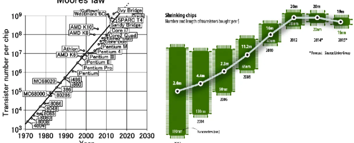
Electronic devices are one of the greatest inventions of the 20th century. Their emergence and development have played a vital role in promoting human society. Microelectronic devices are widely used in various fields and have a strong influence on our lives. Since their invention, electronic devices have undergone the periods of the vacuum tube, the transistor and integrated circuits.1-3 Over the past 40 years, the development of large-scale integrated circuits on chips has led to the shrinkage of the dimensions of electronic devices.
According to the development trend of electronic devices, Moore in 1965 predicted an annual doubling in the number of components per integrated circuit. In the 1980s, he revised the forecast to doubling every two years.4,5 This is the famous "Moore's law".6 The size of a single component on a chip has been decreasing during the past decades. In 2010, a chip on CPU made up of 700 million transistors, where the dimension of a single component was only 40 nm, was created by the Intel company. As can be seen in figure 1.1, the dimension of the components on the chip decreased from 180 nm in 2002 to 16 nm in 2015. Even though shrinkage no longer cut transistor costs from 2012, it is clear that devices were minimized to the nanoscale. With Skylake, the codename used by Intel for a microarchitecture processor, Intel will have virtually minimized the scale to 14 nm by the end of 2016.
2
Recent decades have witnessed a significant development of techniques for the fabrication of nanostructures. The requirement for small devices stimulates the development of nanotechnologies. These technologies can be classified into two categories: top-down and bottom-up methods. Top-down methods, such as patterning and lithography, are based on a large-scale preparation reducing the dimensions to the nanoscale.7,8 An example of a simplified nanofabrication method used to construct 1D nanochannels is presented in reference 9 and shown in figure 1.2. The processes are significantly simplified and sub-50 nm-deep fluidic channels are formed after bonding the nanopatterned wafers with silicon or borofloat-glass wafers.9 On the other hand, bottom-up methods begin with atoms or molecules to build up nanostructures, in some cases through the smart use of self-organization.7 By starting from an atom or a single molecule to complete the integration of the device, nanoscale molecular devices may be realized. This concept evolved from the Feynman's famous statement: "There’s plenty of room at the bottom".10 He put forward the idea of "assemble from individual molecules or atoms". Then a new subject is known as "molecular electronics" emerged.
Figure 1.2. The basic fabrication process of a nanochannel.
When device size is reduced to below 10 nm, quantum effects will be detected.11 Charge transport properties in the component may change from the classical regime to the quantum regime.
What are the classical and the quantum regimes? As illustrated in figure 1.3, when the length (L) and width (W) of the wire are much larger than the electron mean free path (l), electron transport in the nanowire involves collisions and is in the classical regime. Macroscopic conductors are characterized by Ohm’s law: G = σS/L,12
3
intrinsic conductivity of the wire, S is the cross-sectional area, and L is the length of the wire.
Figure 1.3. The classical limit and quantum limit of electron transport through a wire.11
When the mean free path, l, is greater than L, the electron moves ballistically without collision through the nanowire. Furthermore, when the fermi wavelength of the electrons (λF) becomes comparable or larger than the contact diameter, quantum effects will govern the electric transport properties.13 This is the so-called quantum regime. In these cases the metallic nanowire is also named “atomic point contact”.
The electrical conductance through such a metallic nanowire is quantized and is expressed by the Landauer formula14,15:
G =2𝑒2
ℎ ∑ 𝑇𝑖
𝑁
𝑖=1 ,
where e is the electron charge, h is the Planck constant and Ti is the transmission
probability the ith channel. The transmission probability of the conductance channel depends on the chemical valency of the metallic atoms and the precise atomic arrangement of the contact.16,17 It has been frequently observed to be nearly 100% in many cases.13,18-20 As a consequence, the conductance tends to be quantized in near integer multiples of the conductance quantum, G0 = 2e2/h=77.4 µS. According to the I(V) characteristic (Figure 1.4), the atomic contact has ohmic behavior with a slope corresponding to 1G0.21
4
Figure 1.4. Schematic drawing of atomic contact and the current through copper atomic contact is linearly dependent on the voltage.
Charge transport through metal/molecules/metal (MMM) junctions is expressed by a similar formula:
G =2𝑒2
ℎ × 𝑇𝑙× 𝑇𝑟× 𝑇𝑀 ,
where e is the electron charge, h is the Planck constant, Tl, Tr, and Tm is the transmission
probabilities through the left electrode, right electrode, and the molecule, respectively. Unlike atomic contacts, the conductance for a single molecular junction range from 10-5 to 10-1 G0.22 Charge transport through molecular junctions is also described by the I-V characteristics, as shown in Figure 1.5.23 I-V curves show a non-linear relation between the voltage and the current.
5
Figure 1.5 . Schematic illustration of a single molecular junction and typical I-Vbias curves
for oligo(phenylene ethynylene) recorded at a bias voltage below 2 V.23
The mechanism of charge transport through a molecule is described by tunneling24 and hoping theory25. In most cases, where the molecule length is as short as a few nanometers, charge transport properties are described by tunneling theory and the conductance (G) through a single molecule decreases exponentially with the length of the molecule (l). It follows the general relation:
G = 𝐺𝐶𝑒−𝛽𝑙,
where GC is the contact conductance, β is known as the attenuation factor, referring to the
efficiency of charge transport through the molecules.
When the molecular length become longer and exceeds a certain threshold, the contribution of tunneling is gradually replaced by a hopping mechanism. Hopping is believed to be responsible for charge transport along long molecules. The conductance (G) is dependent on the temperature (T) and follows an Arrhenius relation given by:
G ∝ 𝑒∆𝐸⁄𝑘𝑇,
Where ΔE is the hopping activation energy, T refers to temperature, and k is the Boltzmann constant.
6
Tunneling is observed in molecular junctions, occurs with small molecules (usually l < 5 nm) and is independent of temperature.26 It was found that the β value differs from alkyl chain molecules to conjugated molecules.27 Hopping is operative in thicker films or long molecular systems and depends on the temperature. The distinction between hopping and direct tunneling transport is important and depends on the transport distances. If it is greater than a certain value (around 6 nm), conduction will be temperature-dependent.
Figure 1.6 Measurements of molecular wire resistance with CP-AFM. A gold-coated tip was brought into contact with an OPI monolayer on a gold substrate. (A) Semilog plot of
R versus L for the gold/wire/gold junctions. Each data point is the average differential resistance obtained from 10 I-V traces in the range –0.3 to +0.3 V. Error bars, 1 SD. Straight lines are linear fits to the data according to Eq. 1. (Inset) A linear plot of R versus
L, demonstrating linear scaling of resistance with length for the long OPI wires. (B) Arrhenius plot for OPI 4, OPI 6, and OPI 10. Reproduced from reference 28.
Figure 1.6 shows an example from Frisbie et al.28 A series of oligophenyleneimine molecules with lengths from 1.5 to 10 nm was investigated using a conducting probe atomic force microscopy (CP-AFM) as the top contact. It was found that the mechanism of direct-current transport changed from tunneling to hopping as a function of the systematically controlled wire length. As depicted in figure 1.6a, the β value changed from 3 nm-1 for d < 5 nm to 0.9 nm-1 for d > 5 nm, and the observed resistance of the molecular layer increased linearly with length for the longer molecules. The region where β = 0.9 nm-1 was temperature-dependent and tunneling were a negligible contributor, as can be seen in figure 1.6b. Yamada et al.29 investigated temperature-dependent charge transport of oligothiophene molecules. Temperature has no influence on the thiophene molecules with a length of 2.2 nm, where charge transport is governed by tunneling theory. When the molecule length is 6.7 nm, molecular conductance apparently decreases as the temperature drops. The transition between tunneling and hopping mechanisms occurs when the
7
molecular length is around 6 nm. Lacroix and McCreery30 found three distinct transport mechanisms for 4.5–22-nm-thick oligo(thiophene) based layers between carbon contacts. Tunneling operates when d < 8 nm. Activated hopping is observed when d > 16 nm for high temperatures and low bias. A third unique activationless transport mechanism, consistent with field-induced ionization of highest occupied molecular orbitals, operates when d = 8– 22 nm. This phenomenon has also been proved by other investigations.31-33
1.2 Molecular wires, molecular switches, and molecular rectifiers
The size of the components in a microelectronic circuit will be reduced to the scale of a few molecules or even a single molecule. Molecules act as a basic component performing special functions in digital electronic devices.34-37 Functional organic molecules were selected to perform as molecular wires, molecular switches, molecular rectifiers, etc. (Figure 1.7). Those molecules with specific functions are designed in order to integrate molecular functionalities into electrical circuits.
8
1.2.1 Molecular wires
Molecular wires work as a component connecting other functional devices in the molecular electrical nanocircuit. Organic molecules with conjugated structures are widely investigated as molecular wires (Figure 1.7). Effective molecular wires must satisfy the following criteria: first, suitable conductance; second, suitable molecular length; third, suitable linker group at the end of the molecules; fourth, encapsulation to avoid arbitrary electron transfer. In general, molecular wires are structurally classified into two parts: the linker group that connects the electrodes and molecular backbones that offer the electron pathway. The interface between the molecules and the electrodes, including the coupling, contact geometries, and the energy alignment has a strong influence on the conductance of the wires. Both conjugated chains and alkane chains are widely investigated. McCreery et al26 summarized conductance of molecular wires of aliphatic and aromatic molecules (Figure 1.8). It is found that the decay factor β differ from alkane chain to conjugated molecules.
Figure 1.8. Attenuation plots for aromatic and aliphatic molecules in ensemble molecular
junctions. NAB = nitroazobenzene, ONI=oligonaphthalenefluoreneimine.26
1.2.2 Molecular switches
Another important subject in molecular electronics is the construction of reliable molecular switches for memory and logic devices. Molecular switches involve molecules which can change their conductance with external inputs, such as the change of pH,39 redox reactions,40 illuminations,41 etc. The organic molecule used as memory elements are promising to replace the traditional silicon-based transistor in electrical logic circuits.
9
Kim et al.42 reported charge transport through photoswitching molecules. The most common used in photoswitching are sulfur based diarylethene molecules. However, in Kim’s work, sulfur-free diarylethene molecules were developed and studied via electrical and optical measurements as well as density functional theory calculations. The molecules are switched to the open and closed isomers forms using UV/Vis illumination (Figure 1.9). These molecules show different conductance for the open and the closed forms.
Figure 1.9. Switching sulfur-free diarylethene molecules using MCBJ device.
Among those switches, redox-active molecules are often chosen for the design of switch systems with hopefully high on/off ratios. These molecules exhibit different conductivities when switched between their oxidized and reduced forms.28,43-48 It allows one to alter the conductance of individual molecules by controlling their redox states.
Besides organic molecules, conducting polymers (CPs) and oligomers have also attracted much attention for applications in molecular electronic devices. The performances of CPs used as switchable molecular wires are quite encouraging due to their flexible and low-cost characteristics. They are one of the most promising candidates for the replacement of traditional silicon-based materials used in metal oxide semiconductor field-effect transistors (MOSFET). Wrighton et al.49 pioneered a redox polymer as a microelectrochemical transistor to measure the electrical properties between source-drain electrodes by controlling the gate potential.
Tao’s Group contributed to this topic in a series of works. The diagram of the experimental setup is shown in Figure 1.10.46 Polyaniline (PANI) is deposited electrochemically on the tip of an STM. PANI junction is formed when it connect a gold surface filling the electrodes gap with a distance of 20 nm to 100 nm. The STM tip is then pulled up, while the current flowing through the junction is recorded. The conductance
10
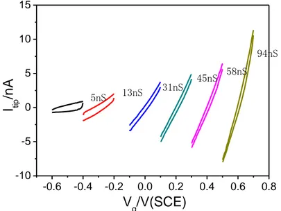
curves recorded during the elongation process of the junction are shown in Figure 1.11. It increases at the beginning and then decreases gradually, and finally, the polymer thread breaks (Figure 1.11a). The conductance levels of 60nS (Figure 1.11b) are due to transitions between stable configurations of the polymer chains induced by the elongation of the junction.
Figure 1.10 Schematic drawing of the nanowire was controlled with respect to a reference electrode. A counter electrode was used as in a standard electrochemical setup. In comparison to a field effect transistor, the RE, WE1, and WE2 electrodes are analogous to
the gate, source and drain electrodes.46
Figure 1.11 (a) conductance of a PANI fiber during elongation process, (b) decrease the zoom increments conductance. Potential of the tip and substrate are now at 0.45 V and 0.5
11
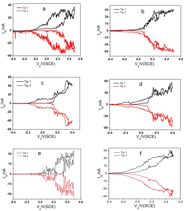
Another experiment forms the same group described the generation of a PANI junction formed between two nano-electrodes separated by a gap in a size of 20 to 80 nm fabricated by lithography with an electron beam.50 When PANI connects the second electrode, the current flowing between the two electrodes suddenly increases. The deposit process is then stopped. Scanning the gate potential (Vg) and applying a fixed bias between the two electrodes, the current through the junctions progressively increases with Vg, and reaches a maximum value at 0.4 V, where it is in the conductive form, as shown in Figure 1.12 a.
Figure 1.12 (a, b, c) of the electrochemical potential function of current for nanojunctions PANI between two gold electrodes separated by about 50 nm (a) and 1 nm (b) and (c). (d)
the characteristic I / V of a nanojunction PANI in the conductive state.50
When the junction is reduced to a few nanometers (Figure 1.11 b and c), instead of a progressive conductance change, an abrupt jump or several abrupt jumps in conductance are observed. At potential less than 0.15V, PANI is in the reduced form (insulating state), no current flows between the electrodes. Increasing the potential to above 0.15 V, the current increases suddenly of several orders of magnitude up to 30 nA (for a bias of 20 mV). The characteristic I / V of nanojunction in conductive form reveals an ohmic behavior and the slope gives the conductance of approximately 400 ns (Figure 1.12d).
Another PANI junctions were studied by Tao et al,51 as shown in Figure 1.13. When the PANI is maintained between 0.05V and 0.15V, the current signal switches drastically between zero and a few tens of nanoamperes. The on/off switching can be controlled by the redox state of the polymer with the potential of the nanoelectrodes. The frequency of the
12
on/off switching is small below 0.1V, and increases as the potential increase, then decrease above 0.15V. At high potentials, the polymer predominately stays in the on state with only occasionally fluctuations to the off state then returning to the on the state.
Figure 1.13 (a) On-off random switching in the conductance of polyaniline ~potential 0.2 V. (b) The dependence of the on-off switch on the potential of the nanoelectrodes. The inset
shows more clearly the on-off switching.
1.2.3 molecular rectifiers
Since 1940, n-doped and p-doped Si has been used as inorganic p-n junction rectifiers on chips. However, flexible materials with high on/off ratios are required for rectifier devices in electric nanocircuits. In 1974 Aviram and Ratner43 proposed the first molecular rectifier model. They believed that molecules with donor (D)-σ-acceptor (A) structure would exhibit rectification properties. Since then the interest in molecular rectification has spread. Because of the difficulties of organic synthesis methodologies, a molecular rectifier using a single molecule with D−σ−A structure (Aviram-Ratner model) has not yet been reported. However, rectifying molecules with D−π−A has been widely investigated.
Molecular rectification is characterized by following the I-V curves. As shown in Figure 1.14, Tao et al.52 used STM break junctions to study charge transport through symmetric tetraphenyl and non-symmetric diblock dipyrimidinyldiphenyl molecules. These nonsymmetric molecules(Figure 1.14b) exhibit rectification behavior (rectifying
13
ratio of 5) as compared to symmetric molecules (Figure 1.14a). note that the rectifying ratio remains small for the real application.
Figure 1.14 Current-voltage (I–V) curves for the symmetric (a) and nonsymmetric
molecules(b).52
In fact, besides the Aviram−Ratner model, several other factors may also lead to molecular rectification phenomena, such as two electrodes of different work functions involved in MMM junctions,53-55 different anchoring groups of the molecules resulting in asymmetric interfacial coupling,56,57 and the contact geometry in the electrode-molecule interface.58,59
1.3 Molecular junctions and atomic contact test-beds
To investigate charge transport through molecular electronic devices, one needs to find a way to wire molecules between the electrodes. Constructing the Metal/Molecule/Metal (MMM) junctions is the basic concept in molecular electronics investigations. In general, the conductivity of the metallic electrode is much higher than the molecules of the MMM junction. As a consequence, the conductance of the entire MMM junction depends on the molecule itself and on the interface between the molecule and the electrode.60 Usually, inert metals such as gold and platinum are used as electrodes, due to their chemical stability in ambient conditions. Molecules containing sulfur and nitrogen as terminal groups anchor the gold and platinum electrodes.
Although it is a long way to achieving commercial molecular electronic devices, many ways have been discovered to study molecular electronics. Recently using bottom-up strategy or sophisticated top-down fabrication has been witnessed. Each MMM fabrication technique has its own unique advantages but still is far from perfect.61 Here we will recall
14
some of the most general techniques and summarize the basic principles in the fabrication of MMM junctions.
1.3.1 Scanning Tunneling Microscope break junction(STM-BJ)
Scanning Tunneling Microscope break junction (STM-BJ)is a technique used for the in situ formation of an MMM junction. It starts with a metallic STM tip located a few nanometers above the substrate electrode. The tip movement is controlled by the piezo traveling toward the substrate electrode. Due to the precise control in the z-direction of the piezo, the gap distance between the tip and the substrate electrodes can be tuned within a few nanometers.
As shown in Figure 1.15a,62 the STM tip repeatedly contacts the substrate. The molecules may bridge both the tip and the substrate electrodes during tip movement. Current versus tip travel time (I-t) curves are recorded (Figure 1.15b). Plateaus are often observed in the I-t curves. Such a plateau represents the transport current value of the molecules involved in the MMM junction.25 The conductance of the single molecule is determined by the current plateau as well as the conductance histogram (Figure 1.15c) which is constructed from a large number of I-t curves.
Figure 1.15. STM-BJ measurements: (a) Schematic depiction of break junction system used for measuring conductance; (b) Several example conductance versus time traces; (c)
Conductance histogram with a peak at the most probable conductance value for a
single-molecule junction.62
Tao’s group pioneered the development ofSTM-BJ for conductance measurement of molecular junctions.24 Figures 1.15a and b show values of conductance quantum recorded
15
when the tip electrode is pulled away from the substrate. It represents the typical conductance traces of Au atomic contacts. Conductance decreases in a stepwise fashion with each step occurring at integer values of G0. The corresponding conductance histogram (Figure 1.16b) shows a well-defined peak at N G0, indicating the formation of a clean Au atomic contact. Next figures 1.15c and d correspond to molecular junction breaking during tip retraction. When the contact shown in (a) is completely broken, corresponding to the collapse of the last quantum step, a new series of conductance steps appears if molecules such as 4,4′- bipyridine are present in the solution. These steps are due to the formation of the molecular junction between the tip and the substrate electrode. Conductance below 1 G0 was observed in Figure 1.16 c. Such conductance values are attributed to charge transport through the molecular junction. The corresponding conductance histogram shows dominant conductance peaks (see Figure 1.16d). Various conductance peaks represent different numbers of molecules involved in the junctions. In the case where no molecules are present in the solution, none of these peaks of low conductance value is observed (Figures 1.15e and f).
Figure 1.16 (A) Conductance of a gold contact formed between a STM gold tip and a gold substrate; (B) Corresponding conductance histogram constructed from 1000 conductance
curves as shown in (A) shows well-defined peaks near 1 G0, 2 G0, and 3 G0 due to conductance quantization; (C) New series of steps that appear after the gold contact is
broken, if molecules such as bipyridine are present in solution; (D) Histogram of conductance measurements obtained for 1000, corresponding to conductance curves of the
same type as in (C); (E) and (F) Conductance curve and histogram when there are no
molecules in solution. 24
This technique has been used by many groups. It can also be used in three-terminal nanoelectronic devices controlling charge transport in a redox-active channel.47,48,63 Leary et al. have shown that conductance switching is obtained in a redox-gated single-molecule junction.64 Venkataraman et al.65 also reported that electrochemical gating directly
16
modulates the alignment of the conducting orbital relative to the metal Fermi energy, thereby changing the single junction transport properties. Zhou et al.66 studied three molecules with various redox centers and found on/off ratios of 2 to 10 when the redox state of the molecules was varied.
1.2.2 Mechanically controlled break junction (MCBJ)
Mechanically controlled break junctions (MCBJ) were first developed by Moreland and Ekin in 1985 to investigate tunneling characteristics.67,68 Then Muller and van Ruitenbeek developed MCBJ to study atomic contacts.69 It was first used for the measurement of single-molecule conductance by Reed et al. in 1997.70
Figure 1.17. The principle of the mechanically controlled break junction (MCBJ) measurement and the formation of a metal-molecule-metal bridge during the breaking
process.71
Figure 1.17 illustrates the basic principle of MCBJ.71 It starts with a notched wire over a bendable substrate, a counter-rod to support the substrate, and a push-rod to break the wire. The substrate is bent by a piezo-controlled push-rod within micrometer precision in the z-direction, while the counter-rod support is kept at the fixed position. After breaking the metal wire, two clean nanoelectrodes are generated face-to-face. The distance between the electrodes for both the opened and the closed directions is controlled by the bending and relaxing of the substrate, respectively.72 In the presence of individual molecules, an MMM junction is probably generated during the mechanical movement. Current versus displacement (I-S) curves are simultaneously recorded. Molecular conductance is determined by the plateaus in the I-S curves as well as the conductance histogram constructed from a large number of individual I-S events, which is similar to that
17
determined by STM-BJ. As a technique for generating MMM junctions, MCBJ has been employed in the measurement of the conductance of a single molecule73,74 as well as the conductance quantum of atomic contacts.75,76
Even though it is difficult to use MCBJ, because it remains a rather sophisticated system compared to STM-BJ, it provides the possibility of combination with other techniques. For example, as shown in Figure 1.18, Tian et al77reported a combined SERS and MCBJ method to measure SERS signals of molecules located inside the nanogap between two electrodes on a Si chip. The distance between electrodes is controlled within several nanometers by MCBJ. Meanwhile, in-situ molecular assembly in the gap is observed by SERS. Such a combination of MCBJ and SERS makes it possible to detect a single or a small number of molecules between two probe electrodes.
Figure 1.18 Study of electrical and optical properties of probe molecule by using mechanically controlled break junction (MCBJ) combined with in-situ surface enhanced
Raman spectroscopy (SERS).
MCBJ is one of the most widely adopted methods in the measurement of molecular electronics. However, MCBJ remains difficult to use and to form stable molecular junctions. This limitation has been recently overcome by Van der Zant et al. They showed that a single molecular junction with high time endurance can be generated by MCBJ.78
1.2.3 Single-wall Nanotubes (SWNT)
A recent method for the fabrication of a molecular junction is based on the so-called single-wall nanotubes (SWNT).79 SWNT have a special structure in chirality and diameter and a simple composition of carbon. Since their discovery more than twenty years ago, nanotubes have stimulated a large amount of research. They can be used as the electrode due to their high conductivity and richness of electrical diversity. There are several methods for creating SWNT nanogap electrodes, including focused-ion-beam etching (FIB), electron beam, electrical breakdown, and lithography-defined oxidative cutting.80-83 As shown in Figure 1.19, an electrode gap was fabricated by cutting the SWNTs using an
18
electron beam.84 A molecular junction was created by amide bond formation between the amines and the carboxylic acid groups that terminate the electrodes. It provides the chemical attachment to span the gap. In this work, it was found that the photo-switching can cycle between the open and closed states.
Figure 1.19. (A) Molecular bridges between the ends of an individual single-walled carbon nanotube (SWNT) electrode; (B) Switching between conjugated and
non-conjugated molecular structures.
Due to their unique physical and chemical properties, such as the nano-size, mechanical strength, toughness, and excellent electrical conductivity, SWNTs have unique advantages in the study of single-molecule devices. It also has an advantage for building horizontal molecular devices with high stability. However, preparing an SWNT electrode is complicated. The yield for the formation of such molecular junctions is only ∼3%.61
1.2.4 Conducting probe atomic force microscopy (CP-AFM)
Conducting probe atomic force microscopy (CP-AFM) is another technique widely used in the investigation of MMM junctions. Frisbie et al.85,86 pioneered the development of this technology. In CP-AFM, as shown in Figure 1.20, an AFM tip, coated with a conductive metal layer (usually Au), is positioned by piezo using feedback based on van der Waals force.87 A nanometric gap is created by approaching the tip to the substrate. MMM junctions are established when the tip contacts a self-assembled molecular monolayer deposited on the substrate. Then charge transport through the junction is followed by applying a bias between the tip and the substrate.
19
Figure 1.20. Typical point-contact CP-AFM experiment in which an Au-coated AFM tip is
used to probe the resistance of a thin crystal of sexithiophene.85
CP-AFM is an extension of the standard AFM set-up. Its major advantage is the ability to control tip-sample separation, providing a tip-sample contact in order to measure the conductance of the SAMs. It gives an MMM junction with high stability. It has been successfully employed in the investigation of large-area molecular junctions by conductance measurements on alkane chains88,89 and conjugated molecules.90,91 However, the tip size of AFM is usually larger than that of STM. The number of molecules involved in the MMM junctions using CP-AFM is usually hard to control. If the substrate electrode is smaller than the AFM tip, the number of molecules involved in the MMM junctions will be limited. Dominique et al92 reported that conductance of alkylthiol molecules was measured by CP-AFM. In this work, a large array of sub-10 nm single crystal Au nanodots electrodes was used as a substrate electrode, which allowing to measure the conductance of up to a million of junctions in a single CP-AFM image.
In this section, we have reviewed some molecular electronics test-beds in the literature. There are still other techniques used in the research of single-molecule junctions and large-area molecular junctions, such as liquid metal contact,93,94 electromigration breakdown junction,95 on-wire lithography,96-98 etc. Comparing those techniques,the basic principles for the fabrication of molecular junctions are quite similar. These techniques share a common structure: an electrode gap that fits the molecular length should be generated, a reliable connection between molecules and the electrode. Single or more molecules are thus sandwiched inside the gap of the electrodes.
20
1.4 Scanning electrochemical microscopy (SECM)
In our group, we plan to investigate charge transport properties through conducting polymer junctions and atomic contacts using scanning electrochemical microscopy (SECM). To do so, a gap between two electrodes is required in order to generate MMM junctions.
1.4.1 Background
Dating back to 1986, Engstrom et al.99 pioneered to approach an ultramicroelectrode (UME) (10 µm in diameter) on a conventional millimeter electrode at a distance of 5 μm. They were able to probe the amperometric response in the diffusion layer of the electrode. In the same year, Bard et al.100 developed a similar technique to study the electrochemical response of a redox probe. In 1989, Bard proposed the name of this technique: Scanning Electrochemical Microscopy (SECM) and published several papers describing the technique and the theory.101,102 Since then, the number of studies employing this technique continues to increase.103-106
1.4.2 SECM principle
Figure 1.21. Schematic principle of SECM
The SECM device is schematically shown in Figure 1.21. This device consists of: - A system with 3 or 4 electrodes: a working electrode (UME), a counter electrode, a reference electrode and optionally a second working electrode that is used as the substrate;
Potential Programmer Tip potential Reference Electrode Counter Electrode Substrate Potential Bipotentiostat Piezo Controller Piezo Positioner x y z
21
- A piezo-controlled positioning system permitting movement of the UME tip relative to the substrate in three dimensions;
- A potentiostat or bipotentiostat to monitor or measure the potential and current.
The monitored signal of the SECM is the electrochemical current on the microelectrode tip. When the tip is moved close to the surface of a sample, disruption of current provides information about the nature and electrochemical properties of the substrate.
When a UME (disk shape) is immersed in a supporting electrolyte containing a redox system, the current through the UME during a potential sweep gives the signal, as shown in Figure 1.22.
Figure 1.22. Distribution of species and their electrochemical reaction on the UME and cyclic voltammetry response of a redox system on UME.
The diffusion-controlled current on the UME is given by the formula:
It, inf = 4nFDCa,
Where n is the number of electrons exchanged during the electrochemical reaction (Ox + ne -= R), F is Faraday's constant, D is the diffusion coefficient of the redox species in solution, C is the concentration of the redox system, and a is the radius of the UME.
This expression is valid when the UME is far from the surface and nothing disrupts diffusion of the redox species to its surface. As the tip get close to the substrate the electrochemical current change. The current variation depends on the distance between the tip and the substrate. The shape of the approach curve gives information on the reactivity of the substrate.
22
Figure 1.23 (a)Regeneration of the mediator on a conductive substrate and (b) the approach curve.
Figure 1.23 shows the schematic approach of a UME to a conductive substrate and the corresponding approach curve. When the UME approaches a conductive surface, the oxidized redox mediator to the tip broadcasts to the conductive substrate, where it is reduced, and then diffused again in the vicinity of the UME. The mediator is thus regenerated close to the probe, causing an increase in the flow of the reactive species arriving on the UME. Therefore, the oxidation current at the tip increases as the UME approaches the surface, as shown in Figure 1.23, this is called "positive feedback".
Figure 1.24 shows a schematic approach of a UME to an insulating substrate and the corresponding approach curve. In this case, the surface is insulating and chemically inert. When the approach distance is reduced, the diffusion of the mediator to the UME is particularly hampered by the insulating body of the surface. The current at the UME is reduced as the tip approaches the surface. As shown in Figure 1.24, this is called "negative feedback".
Figure 1.24. (a)Regeneration of the mediator on an insulating substrate and (b) the approach curve.
Conductor
R
O
-e
-R
O
-e
-d
a
Insulator
R
O
-e
-×
d
a
23
1.4.2.1 Theoretical tip approach
The theory of the regeneration mode proposed by Kwak and Bard102 is based on the numerical solution of diffusion equations. In many cases, analytical approximations allow a much simpler solution. The following theoretical results are for a disc-shaped electrode. The theoretical approach curves were obtained by simulating the approach of the UME to the substrate, and reflect the evolution of the current iT depending on the distance d separating from the substrate. These curves are characteristic of the nature of the substrate and redox processes occurring there. They are usually displayed in their normalized form, with IT = iT/iT,inf andL = d/a. In this way, the approach curves are independent of the electrode radius a, the diffusion coefficient D and the mediator concentration C. The analytical expression of the approach curve on an insulating substrate is given by:
IT,insulating(L) = 1/{0.15 + (1.5358/L) + 0.58exp(-1.14/L) + 0.0908exp [(L-6.3)/(1.017L)]},
and the expression for the approach curve on a conductive substrate is given by:
IT,conducting (L) = 0.68 + (0.78377/L) + 0.3315exp(-1.0672/L).
1.4.2.2 Experimental tip approach
After the UME is immersed in a solution containing a reversible redox couple, the current at the UME is recorded as it approaches the surface. Depending on the nature of the substrate, the current increases (decreases) when the UME comes close to the conductive (insulating) substrate surface. The approach is then automatically stopped at a set value. Efforts have been focused on the fabrication of smaller tips, with radius of the order of a few nanometres, with the aim of achieving a close approach, even at L = 0.2.107,108 It has been reported by Bard et al. that tip-to-substrate gaps of d = 110 nm can be achieved.107 In the context of this Ph.D, a controlled size gap can be easily formed between a UME and another electrode by recording the approach curve in the presence of a redox mediator.
1.4.2.3 Molecular junctions by SECM
Since a controlled size gap can be easily formed between UME and another electrode, metal or a conductive polymer can be deposited to connect the probe and the substrate. The SECM setup seems to favor the manufacturer of junctions or metallic contact.
In the previous work in our group, it has been clearly observed that a separate charge transfer and charge transport processes occur in a redox gated polyaniline (PANI)
24
nanojunction.109 And even a PANI junction where charge transport is controlled by a single oligoaniline strand was obtained. SECM, is also proposed as a tool for the fabrication of copper atomic point contact.110 The formation of atomic contacts is supported by the ohmic behavior of the I–V curve. It depends neither on the UME tip radius nor on the initial gap size between tip and substrate.
The redox gated conducting polymers molecular junctions and atomic point contacts studied in this thesis will be created by electrochemical method using SECM.
1.5 Summary
In this chapter, we briefly discussed the historical development of molecular electronics and a few relevant concepts, as well as the experimental techniques developed over the past decades. We recalled the basic theory of electron transport in the classical regime and quantum regime. Furthermore, we mentioned the techniques to create molecular junctions. We introduced the basic principle of the SECM set-up. This thesis is based on the expertise of the Nano Electrochemistry’s (NEC) group in nanoscale electrochemistry. In my Ph.D. work, SECM will be used to generate MMM junctions. The thesis focuses on several scientific issues which have been expressed in the general introduction and will be presented in details in the next chapters.
REFERENCES
1 Lee, T. H. The design of CMOS radio-frequency integrated circuits. (Cambridge university press, 2003).
2 Kilby, J. S. Invention of the integrated circuit. Electron Devices, IEEE Transactions
on 23, 648-654 (1976).
3 Nishizawa, J.-i., Terasaki, T. & Shibata, J. Field-effect transistor versus analog transistor (static induction transistor). Electron Devices, IEEE Transactions on 22, 185-197 (1975).
4 Moore, G. E. in Electron Devices Meeting. 11-13.
5 Marwala, T. Impact of Artificial Intelligence on Economic Theory. arXiv preprint
arXiv:1509.01213 (2015).
6 Schaller, R. R. Moore's law: past, present and future. Spectrum, IEEE 34, 52-59 (1997).
7 Mijatovic, D., Eijkel, J. & Van Den Berg, A. Technologies for nanofluidic systems: top-down vs. bottom-up—a review. Lab on a Chip 5, 492-500 (2005).
8 Walsh, S. T. Roadmapping a disruptive technology: A case study: The emerging microsystems and top-down nanosystems industry. Technological Forecasting and
25
9 Haneveld, J., Jansen, H., Berenschot, E., Tas, N. & Elwenspoek, M. Wet anisotropic etching for fluidic 1D nanochannels. Journal of Micromechanics and
Microengineering 13, S62 (2003).
10 Feynman, R. P. There's plenty of room at the bottom. Engineering and science 23, 22-36 (1960).
11 Davenport, N. Observations of Quantized Conductance over Nanowires. (2013). 12 Onsager, L. Deviations from Ohm's law in weak electrolytes. The Journal of
Chemical Physics 2, 599-615 (1934).
13 Agraıt, N., Yeyati, A. L. & van Ruitenbeek, J. M. Quantum properties of atomic-sized conductors. Physics Reports 377, 81-279 (2003).
14 Landauer, R. Spatial variation of currents and fields due to localized scatterers in metallic conduction. IBM Journal of Research and Development 1, 223-231 (1957). 15 Büttiker, M., Imry, Y., Landauer, R. & Pinhas, S. Generalized many-channel conductance formula with application to small rings. Phys. Rev. B 31, 6207 (1985). 16 Bogozi, A. et al. Molecular adsorption onto metallic quantum wires. Journal of the
American Chemical Society 123, 4585-4590 (2001).
17 Scheer, E. et al. The signature of chemical valence in the electrical conduction through a single-atom contact. Nature 394, 154-157 (1998).
18 Ohnishi, H., Kondo, Y. & Takayanagi, K. Quantized conductance through individual rows of suspended gold atoms. Nature 395, 780-783 (1998).
19 Rodrigues, V., Fuhrer, T. & Ugarte, D. Signature of atomic structure in the quantum conductance of gold nanowires. Phys. Rev. Lett. 85, 4124 (2000).
20 Agraït, N., Untiedt, C., Rubio-Bollinger, G. & Vieira, S. Onset of energy dissipation in ballistic atomic wires. Phys. Rev. Lett. 88, 216803 (2002).
21 Boussaad, S. & Tao, N. Atom-size gaps and contacts between electrodes fabricated with a self-terminated electrochemical method. Applied Physics Letters 80, 2398-2400 (2002).
22 Marqués-González, S. & Low, P. J. Molecular Electronics: History and Fundamentals. Australian Journal of Chemistry 69, 244-253 (2016).
23 Xiao, X., Nagahara, L. A., Rawlett, A. M. & Tao, N. Electrochemical gate-controlled conductance of single oligo (phenylene ethynylene) s. Journal of
the American Chemical Society 127, 9235-9240 (2005).
24 Xu, B. & Tao, N. J. Measurement of single-molecule resistance by repeated formation of molecular junctions. Science 301, 1221-1223 (2003).
25 Tao, N. Electron transport in molecular junctions. Nature nanotechnology 1, 173-181 (2006).
26 McCreery, R. L., Yan, H. & Bergren, A. J. A critical perspective on molecular electronic junctions: there is plenty of room in the middle. Physical Chemistry
Chemical Physics 15, 1065-1081 (2013).
27 Wu, S. et al. Molecular junctions based on aromatic coupling. Nature
nanotechnology 3, 569-574 (2008).
28 Choi, S. H., Kim, B. & Frisbie, C. D. Electrical resistance of long conjugated molecular wires. Science 320, 1482-1486 (2008).
29 Lee, S. K., Yamada, R., Tanaka, S. & Tada, H. Electrical Conductance of Single Oligothiophene Molecular Wires: Temperature Effect. Mater. Res. Soc. Symp. Proc. 1286 (2011).
30 Yan, H. et al. Activationless charge transport across 4.5 to 22 nm in molecular electronic junctions. PANS 110, 5326-5330 (2013).
31 Lee, S. K. et al. Universal temperature crossover behavior of electrical conductance in a single oligothiophene molecular wire. ACS nano 6, 5078-5082 (2012).