HAL Id: tel-01672814
https://hal.inria.fr/tel-01672814
Submitted on 27 Dec 2017
HAL is a multi-disciplinary open access archive for the deposit and dissemination of sci-entific research documents, whether they are pub-lished or not. The documents may come from teaching and research institutions in France or abroad, or from public or private research centers.
L’archive ouverte pluridisciplinaire HAL, est destinée au dépôt et à la diffusion de documents scientifiques de niveau recherche, publiés ou non, émanant des établissements d’enseignement et de recherche français ou étrangers, des laboratoires publics ou privés.
Methodology and Tools for Energy-aware Task Mapping
on Heterogeneous Multiprocessor Architectures
Baptiste Roux
To cite this version:
Baptiste Roux. Methodology and Tools for Energy-aware Task Mapping on Heterogeneous Multipro-cessor Architectures. Embedded Systems. Université de Rennes 1, 2017. English. �tel-01672814�
ANNÉE 2017
THÈSE / UNIVERSITÉ DE RENNES 1
sous le sceau de l’Université Bretagne Loire
pour le grade de
DOCTEUR DE L’UNIVERSITÉ DE RENNES 1
Mention : Traitement du signal et Télécommunications
Ecole doctorale MathSTIC
présentée par
Baptiste Roux
préparée à l’unité de recherche IRISA (UMR 6074)
Institut de Recherche en Informatique et Systèmes Aléatoires
École Nationale Supérieure des Sciences Appliquées et de
Technologie
Methodology and Tools
for Energy-aware Task
Mapping on
Heterogeneous
Multiprocessor
Architectures
Thèse soutenue à Rennes le 23 novembre 2017 devant le jury composé de :
Virginie FRESSE
MCF - Université Jean Monnet / rapporteur
Frédéric ROUSSEAU
PR - Université Grenoble Alpes / rapporteur
Jean-Philippe DELAHAYE
Ingénieur - DGA MI / examinateur
Bertrand GRANADO
PR - Université Pierre et Marie Curie / examinateur
Loic LAGADEC
PR - ENSTA Bretagne / examinateur
Matthieu GAUTIER
MCF - Université Rennes 1 / co-directeur de thèse
Olivier SENTIEYS
Résumé
Au cours de la dernière décennie, la conception des systèmes embarqués a évolué dans l’op-tique d’augmenter la puissance de calcul tout en conservant une faible consommation d’énergie. À titre d’exemple, les véhicules autonomes tels que les drones sont un domaine d’application re-présentatif qui combine de la vision, des communications sans fil avec d’autres noyaux de calculs intensifs, le tout avec un budget énergétique limité. Avec l’avènement des systèmes multicœurs sur puce (MpSoC), la simplification des processeurs a diminué la consommation d’énergie par opération, alors que leur multiplication a amélioré les performances. Cependant, l’apparition du phénomène de dark silicon a conduit à l’intégration d’accélérateurs matériels spécialisés au sein des systèmes multicœurs. C’est ainsi que sont nées les architectures massivement multicœurs hétérogènes (HMp-SoC) combinant des processeurs généralistes (SW) et des accélérateurs matériels (HW). Pour ces architectures hétérogènes, les performances et la consommation d’énergie dépendent d’un large en-semble de paramètres tels que le partitionnement HW/SW, le type d’implémentation HW et le coût de communication entre les organes de calcul HW et SW conduisant ainsi à un immense espace de conception.
Dans cette thèse, nous étudions des méthodes permettant la réduction de la complexité de dé-veloppement et de mise en œuvre d’applications efficaces en énergie sur HMpSoC. De nombreuses contributions sont proposées pour améliorer les outils d’exploration de l’espace de conception (DSE) avec des objectifs énergétiques. Tout d’abord, une définition formelle de la structure HMpSoC est in-troduite ainsi qu’une méthode de représentation générique axée sur la hiérarchie mémoire. Ensuite, un outil de modélisation rapide de l’énergie est proposé et validé sur plusieurs applications. Ce mo-dèle énergétique sépare les sources d’énergie en trois catégories (calcul statique, dynamique et com-munications) et calcule leurs contributions sur la consommation globale de manière indépendante. Basée sur une étude précise des communications, cette approche calcule rapidement la consom-mation d’énergie pour une répartition donnée d’application sur un HMpSoC. Dans un deuxième temps, nous proposons une méthodologie permettant l’exploration énergétique d’accélérateurs sur HMpSoC. Cette méthode s’appuie sur le modèle de consommation précédent couplé à une formu-lation de programmation linéaire en nombre entier mixte (MILP). Cela permet de sélectionner effi-cacement les accélérateurs HW et le partitionnement HW/SW et ainsi d’obtenir une implémenta-tion efficace en énergie pour une applicaimplémenta-tion tuilée. Les expériences réalisées ont montré la com-plexité du processus de validation d’outils/algorithmes de DSE sur une large gamme d’applications et d’architectures. Afin de résoudre ce problème, nous proposons un simulateur d’architectures HMp-SoC intégrant un modèle de consommation permettant d’observer l’exécution d’applications. La structure de l’architecture cible est décrite à l’aide d’un fichier de configuration basé sur le modèle de représentation générique précédent. Ce fichier est chargé dynamiquement lors du démarrage du simulateur. De plus, ce simulateur est associé à un générateur d’applications permettant la créa-tion d’un large ensemble d’applicacréa-tions représentatives du domaine. Ce générateur se base sur un ensemble de schémas de calcul et de communication élémentaire qu’il combine pour obtenir une ap-plication complète. Les apap-plications ainsi obtenues peuvent être enrichies par des informations de placement et automatiquement exécutées sur le simulateur. Cet ensemble d’outils a pour objectif de faciliter la validation de nouveaux algorithmes ciblant le placement efficace en énergie d’application sur une large gamme d’architectures HMpSoC.
Abstract
During the last decade, the design of embedded systems was pushed to increase computational power while maintaining low energy consumption. As an example, autonomous vehicles such as drones are a representative application domain which combines vision, wireless communications and other computation intensive kernels constrained with a limited energy budget. With the ad-vent of Multiprocessor System-on-Chip (MpSoC) architectures, simplification of processor cores decreased power consumption per operation, while the multiplication of cores brought performance improvement. However, the dark silicon issue led to the benefit of augmenting programmable pro-cessors with specialized hardware accelerators and to the rise of Heterogeneous MpSoC (HMpSoC) combining both software (SW) and hardware (HW) computational resources. For these heteroge-neous architectures, performance and energy consumption depend on a large set of parameters such as the HW/SW partitioning, the type of HW implementation or the communication cost between HW and SW cores therefore leading to a huge design space.
In this thesis, we study how to reduce the development and implementation complexity of energy-efficient applications on HMpSoC. Multiple contributions are proposed to enhance Design Space Exploration (DSE) tools with energy objectives. First, a formal definition of HMpSoC struc-ture is introduced alongside with a generic representation focused on the memory hierarchy. Then, a fast power modelling tool is proposed and validated on several applications. This power model separates the power sources in three families (static, dynamic computation and dynamic communi-cation) and computes their contributions on global consumption independently. With a fine grain communications study, this approach rapidly computes energy consumption for a given application mapping on a HMpSoC. In a second time, we propose a methodology for energy-driven accelerator exploration on HMpSoC. This method builds upon the previous power model coupled with an Mixed Integer Linear Programming (MILP) formulation and enables to efficiently select HW accelerators and HW/SW partitioning which achieve energy efficient-mapping of a tiled application. The exper-iments involved in these contributions show the complexity of DSE validation process on a wide range of applications and architectures. To address these issues, we introduce a HMpSoC simulator embedding a power model to monitor application execution. Properties of targeted architectures are described, at run-time with the previous generic representation model. Furthermore, this simulator is coupled with an application generator framework that could build an infinite set of representative applications following predefined computation models. The obtained applications could then be en-riched with mapping directive and executed on the simulator. This combination enables to ease the research and validation of new DSE algorithms targeting energy-aware application mapping on a wide range of HMpSoC architectures.
Contents
0 Résumé étendu 1
1 Contexte général . . . 1
1.1 Radio logicielle . . . 2
1.2 Tendances architecturales . . . 2
2 Architectures et applications cibles . . . 3
2.1 Architectures cibles . . . 3
2.2 Structure des applications . . . 4
3 Flot de conception & Contributions . . . 5
3.1 Extraction du parallélisme . . . 5
3.2 Creation de l’EPDG . . . 5
3.3 Estimation de l’énergie . . . 6
3.4 Exploration de l’espace de conception . . . 6
3.5 Platforme d’émulation de HMpSoC . . . 8
4 Conclusion . . . 8
1 Introduction 11 1 General context . . . 11
1.1 Software-Defined Radio . . . 12
1.2 DVB-S2: a relevant SDR application example . . . 12
2 Technology progress and architecture trends . . . 14
2.1 Towards the integration of dedicated HW accelerators . . . 14
2.2 Energy efficiency: the next challenge of embedded systems . . . 15
3 Contributions of the Thesis . . . 15
4 Organization of the document . . . 16
2 Heterogeneous Architectures: Structures and Applications 19 1 Survey on MpSoC architectures . . . 19
1.1 Dedicated SDR architectures . . . 20
1.2 General Purpose architectures . . . 21
2 Generic HMpSoC representation . . . 25
2.1 Generic HMpSoC architecture . . . 25
2.2 Oriented tree for memory hierarchies . . . 26
3 Application structure and representation . . . 27
3.1 Parallelism-Level . . . 27
3.2 Data Flow programming models . . . 28
3.3 Control Flow programming models . . . 30
3.4 Mixed programming models . . . 30
4 Generic application structure . . . 32
3 Power Modelling and Computer-Aided Design Tools 35 1 Power modelling facilities . . . 35
CONTENTS
1.1 Low-level estimation techniques . . . 36
1.1-1 Circuit/Transistor level . . . 36
1.1-2 Logic/Gate level . . . 37
1.1-3 Register Transfer level . . . 37
1.2 High-level estimation techniques . . . 37
1.2-1 Architectural-level . . . 38
1.2-2 Functional-level . . . 39
2 Computer Aided Design tools . . . 41
2.1 Parallelism-extraction . . . 41
2.1-1 Algorithms . . . 41
2.1-2 Frameworks and Tools . . . 43
2.2 HMpSoC Design Space exploration . . . 45
2.2-1 Simulation-based DSE . . . 45
2.2-2 Analytical-based DSE . . . 46
2.2-3 Hardware focused DSE . . . 47
4 Fast Power Modeling for HMpSoC 55 1 Communication-Based Power Model . . . 55
1.1 Computation energy cost . . . 56
1.2 Communication energy cost . . . 57
1.3 Static energy cost . . . 57
2 Deep-dive on two Architectures . . . 58
2.1 Micro-benchmark principle . . . 58
2.1-1 General structure of a micro-benchmark set . . . 58
2.2 Kalray MPPA . . . 59 2.2-1 MPPA structure . . . 60 2.2-2 Power analysis . . . 61 2.3 Xilinx Zynq . . . 66 2.3-1 Zynq structure . . . 66 2.3-2 Power analysis . . . 67
3 Power model validation on Xilinx zynq . . . 74
3.1 The mutant application principle . . . 74
3.2 Mutant validation . . . 74
4 Conclusion . . . 76
5 Energy-Driven Accelerator Exploration for HMpSoC 79 1 Overview of Proposed Tiled-DSE Flow . . . 80
1.1 Tiling-based parallel applications . . . 80
1.2 Heterogeneous Architectures . . . 82
1.3 Tiled-DSE Objectives . . . 82
1.4 Energy and execution time models . . . 83
1.4-1 Computation time . . . 83
1.4-2 Energy consumption . . . 83
2 Computation Parameter Extraction . . . 84
3 Design Space Exploration of Tiled Applications . . . 84
3.1 Exhaustive search . . . 85
3.2 MILP formulation . . . 86
3.2-1 Model constraints . . . 86
3.2-2 Cost functions . . . 87
CONTENTS 4 Experimental Setup . . . 89 4.1 Application kernels . . . 89 4.2 Measurement infrastructure . . . 89 4.3 Hardware implementations . . . 89 4.4 Software implementations . . . 92 5 Exploration Results . . . 92 5.1 Parameter extraction . . . 93 5.2 MILP optimization . . . 93
5.3 Precision and gain factors . . . 94
6 Conclusion . . . 95
6 HMpSoC Emulation Platform 97 1 Motivations . . . 97
2 Architecture emulation layer . . . 98
2.1 Underlying technologies . . . 98
2.1-1 QEMU . . . 98
2.1-2 SystemC . . . 100
2.1-3 SystemC and QEMU association . . . 102
2.2 Emulator structure . . . 104
2.2-1 Cluster structure . . . 104
2.2-2 NoC structure . . . 105
2.2-3 Configuration facilities . . . 108
2.3 Execution framework and cluster management . . . 108
2.3-1 Communication monitoring . . . 108
2.3-2 NoC management . . . 110
2.3-3 Execution scheme . . . 110
3 Application layer . . . 111
3.1 Representative applications: the dwarf principle . . . 111
3.2 Dwarfs implementation within the execution structure . . . 113
3.2-1 Wrapper structure and communication scheme . . . 113
3.2-2 SW implementations . . . 114
3.2-3 HW implementations . . . 114
3.3 Generic graph generation . . . 114
3.3-1 Generator structure . . . 114
3.3-2 Graph execution and monitoring facilities . . . 115
3.4 Communication energy monitoring results . . . 116
4 Conclusion . . . 117
7 Conclusion & Perspectives 119 1 Conclusion . . . 119
2 Perspectives . . . 121
I
Appendices
123
A Manual loop-nest modification 125
B HMpSoC configuration file 127
CONTENTS Publications 133 Bibliography 135 List of Figures 144 List of Tables 145 Acronymes 148
Chapitre
zéro
RÉSUMÉ ÉTENDU
1
Contexte général
Les systèmes embarqués ont par définition des ressources énergétiques limitées. Un des verrous à l’augmentation des débits des objets communicants et embarqués est de pouvoir réaliser un nombre important de traitements sous cette contrainte d’énergie finie ou de puissance dissipée maximale. La mise en œuvre de la liaison de données entre les drones et une station de base terrestre est une application qui entre dans ce contexte. En effet, la gestion de l’énergie est un verrou limitant la durée des missions de ces drones. Ainsi, réduire la consommation des traitements numériques embarqués est un challenge important.
Cette thèse a été cofinancée par l’Institut National de Recherche en Informatique et en Automa-tique (INRIA) et la Direction Générale de l’Armement (DGA). Cette étude est née de besoins inhé-rents aux applications embarquées dans les drones de la DGA. Ces derniers utilisent un lien radio basé sur le standard DVB-S2 avec une architecture matérielle standard basée sur l’association d’un FPGA, d’un DSP et d’un processeur généraliste. L’utilisation de ces trois composants distincts com-plexifie le processus de reconfiguration et diminue les performances énergétiques globales. Cette thèse a pour but d’explorer les opportunités offertes par les nouvelles architectures hétérogènes as-sociant processeurs généralistes et accélérateurs matériels avec le paradigme de communications reconfigurables basé sur la radio logicielle. L’objectif premier est de mettre en avant les forces et les faiblesses de ces architectures et de soulever les difficultés liées à la conception d’applications efficaces en énergie sur ces architectures hétérogènes. À long terme, nous voulons proposer une formalisation de ces architectures ainsi que des outils et des méthodes facilitant le développement d’applications économes en énergie sur ces architectures.
Dans ce chapitre, nous résumons le contexte de l’étude ainsi que les différentes contributions apportées au cours de la thèse. Dans les sous sections suivantes, nous présentons le concept de radio logicielle et les différentes avancées dans le monde de la microélectronique ayant entraîné l’appa-rition des architectures hétérogènes. La section 2 introduit la structure générique des architectures considérées ainsi qu’une méthode de représentation mettant l’accent sur les canaux de communica-tions. Nous présentons également le format de représentation utilisé pour la description d’applica-tion. Enfin, nous introduisons un flot de développement orienté sur l’énergie ainsi que les travaux réalisés au vu de son adoption. Pour finir, la section 4 résume les différents éléments présentés dans ce document.
Section 1 — Contexte général Air interface Reception Microprocessor ADC Transmission Microprocessor DAC
Figure 0-1 – Structure globale d’une radio logicielle idéale.
1.1
Radio logicielle
Le concept de radio logicielle trouve ses fondements dans le domaine militaire avec la néces-sité d’assurer l’inter-opérabilité des équipements à l’aide de plateformes pouvant générer plusieurs formes d’ondes et normes de communication grâce à une simple reprogrammation. En effet, le cycle de vie des applications militaires est assez long et il est essentiel de les maintenir et d’assurer leur inter-opérabilité avec les applications à venir. Ce concept a été introduit pour la première fois dans les années 90 par Joseph Mitola [Mit93]. Il consiste à réduire la partie analogique à son strict mi-nimum pour avoir plus de flexibilité de reconfiguration avec la partie numérique. Une architecture de radio logicielle idéale serait composée d’un convertisseur placé directement derrière l’antenne et d’un composant numérique programmable tel qu’un microprocesseur dédié aux traitements. Cela est illustré sur la Figure 0-1. Cette structure, permettant une flexibilité totale, est l’objectif ultime d’un système de radio logicielle. Malheureusement, numériser le signal juste après l’antenne requière une haute fréquence d’échantillonnage des convertisseurs et représente un frein. De plus, les implémen-tations de radio logicielle basées sur des microprocesseurs généralistes présentent certaines limites notamment liées aux performances énergétiques et aux débits atteignables. Néanmoins, la plupart des algorithmes utilisés est hautement parallèle et nécessite des performances de calculs impor-tantes qui pourraient tirer profit des nouvelles architectures multicœurs hétérogènes et ainsi traiter les problèmes de consommation d’énergie au prix d’une programmation plus complexe.
1.2
Tendances architecturales
Par le passé, la loi de Moore [Moo65] prédisant le doublement du nombre de transistors sur puce tous les 18 mois, a été un moteur fondamental de l’évolution des microarchitectures. Associée à la loi de Dennard [Den+74] prédisant la diminution de la tension et du courant d’alimentation des tran-sistors en proportion de leur taille, une série de circuits, d’architectures et de compilateurs a émergé, conduisant ainsi à une augmentation exponentielle des performances. Ces dernières ont été obtenues en passant progressivement d’architectures simple-cœur à des architectures multicœurs pour tirer pleinement profit du nombre de transistors disponibles. Malheureusement, un nouveau phénomène appelé “dark silicon” lié à la limitation de la densité de puissance dissipée sur une puce [Esm+11] est apparu. Ce dernier empêche l’utilisation simultanée de l’ensemble des transistors présents sur la puce et a poussé les concepteurs d’architectures à intégrer des accélérateurs matériels au sein des microarchitectures. C’est ainsi que sont nées les architectures multicœurs hétérogènes inté-grant plusieurs cœurs processeurs et des accélérateurs matériels. Outre le gain en performance, ces architectures ont induit de nouvelles problématiques en termes de développement. En effet, avec la multiplication du nombre et du type d’organes de calcul, l’espace d’exploration est devenu immense. Ainsi, lorsque la consommation devient un facteur clé, il est essentiel de pouvoir explorer cet espace au plus tôt dans le flot de développement pour obtenir des solutions efficaces en énergie.
Chapitre 0 — Résumé étendu HW Memory unit processor unit 1 processor unit n NoC NoC N o C ... ... ... ... SW 1 NoC_itf Memory unit SW ... processor unit 1 MEMORY SW 2 SW N GPIO DDR N o C Memory unit processor unit 1 processor unit n Memory unit processor unit 1 GPIO DDR Memory unit processor unit 1 processor unit n Memory unit processor unit 1 GPIO DDR Memory unit processor unit 1 processor unit n Memory unit processor unit 1 GPIO DDR HW SW 1 NoC_itf PU ... MEMORY SW 2 PU N HW SW 1 NoC_itf SW ... MEMORY SW 2 SW N HW SW 1 NoC_itf SW ... MEMORY SW 2 SW N
(a) HMpSoC distribué.
HW Memory unit hardware unit A processor unit 1 processor unit n NoC NoC N o C ... ... ... ... NoC_itf Memory unit processor unit 1 MEMORY GPIO DDR SW 0 N o C GPIO DDR GPIO DDR SW 1 SW 2 SW 3 SW ... SW N NoC_itf MEMORY SW 0 SW 1 SM 2 SW 3 SW ... SM N NoC_itf MEMORY SW 0 SW 1 SW 2 SW 3 SW ... SW N NoC_itf (b) HMpSoC partagé. Figure 0-2 – Structure des architectures HMpSoC.
2
Architectures et applications cibles
Dans cette section, nous présentons le formalisme utilisé dans la suite du document pour décrire les architectures et les applications utilisées.
2.1
Architectures cibles
Pour que notre étude puisse être appliquée à un large panel d’architectures, nous avons com-mencé par décrire de manière générique la structure des architectures ciblées. Pour cela, nous avons étudié diverses architectures utilisées dans le domaine de la radio logicielle ainsi que des archi-tectures plus généralistes. Les archiarchi-tectures multicœurs sont généralement composées d’un en-semble de mémoires, de processeurs, d’éléments d’interconnexion et d’entrées/sorties. Lorsqu’elles intègrent des accélérateurs matériels, elles deviennent hétérogènes dans le sens où elles associent des processeurs généralistes (SW) et des accélérateurs matériels (HW). Une représentation générique de ces architectures, appelées HMpSoC, est proposée dans la Figure 0-2. Elle est construite à l’aide de clusters connectés par un réseau sur puce (NoC). Chaque cluster est composé de N cœurs de calcul logiciels associés à un accélérateur matériel de taille S. Au niveau du cluster, les communications sont effectuées grâce à une mémoire partagée. Suite à cette description, deux familles de HMpSoC peuvent être construites en fonction du placement des accélérateurs matériels dans l’architecture. Dans le cas où ils sont placés au sein de chaque cluster (S , 0), on obtient des HMpSoC distribués (Figure 0-2a). Ils permettent d’obtenir des communications rapides entre la partie matérielle et la partie logicielle mais en conséquence, la taille maximale des accélérateurs est réduite. Dans le cas où les accélérateurs sont placés au niveau cluster, on obtient deux types de cluster : les clusters logiciels (N , 0 et S = 0); et les clusters matériels (S , 0 et N = 0). Les architectures ainsi obtenues sont appelées HMpSoC partagés (Figure 0-2b). Cette approche permet d’avoir des accélérateurs matériels de grande taille et de les partager entre les clusters. En contrepartie, ils induisent une augmentation des temps de communications entre la partie logicielle et la partie matérielle.
Les familles de HMpSoC introduites précédemment peuvent définir un grand nombre d’archi-tectures. Pour cibler, avec précision, une architecture particulière au sein de ces familles, nous avons
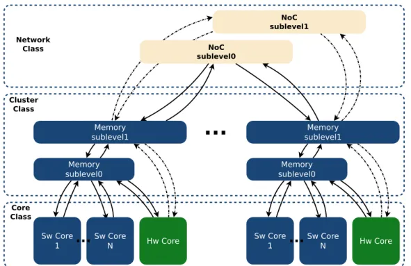
Section 2 — Architectures et applications cibles Sw Core 1 Memory sublevel1 NoC sublevel0 Memory sublevel0 NoC sublevel1 Sw Core 1 Sw Core N Memory sublevel1 Memory sublevel0 Network Class Cluster Class Core Class
...
Sw Core N...
Hw Core...
Hw CoreFigure 0-3 – Représentation d’un HMpSoC basée sur la hiérarchie mémoire.
besoin d’une représentation générique. Pour cela, nous avons proposé une représentation basée sur la hiérarchie mémoire décrite à l’aide d’un arbre orienté (Figure 0-3). Cette représentation divise la hiérarchie mémoire d’un HMpSoC en trois niveaux principaux : réseau, cluster et cœur. Chaque niveau contient des sous-niveaux, avec les propriétés suivantes.
• Au niveau réseau, les sous-niveaux sont disjoints de façon à ce que chaque sous-niveau puisse être utilisé indépendamment.
• Au niveau cluster, les sous-niveaux sont mixtes, c’est-à-dire qu’ils sont liés entre eux mais restent accessibles à chaque sous-niveau.
• Au niveau cœur, les sous-niveaux sont liés. L’accès au sous-niveau de profondeur L passe par les L − 1 sous-niveaux supérieurs.
Pour décrire avec précision une architecture cible, les caractéristiques de chaque classe mémoire doivent être définies, telles que la profondeur de chaque sous-niveau, le débit des canaux, ainsi que le coût des communications.
2.2
Structure des applications
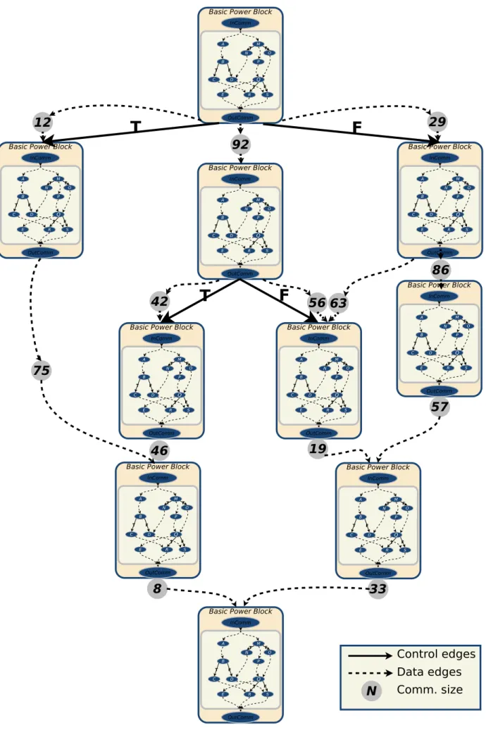
Après une étude des paradigmes de représentation des applications, nous formalisons la repré-sentation qui sera utilisée dans le cadre de ce travail. Cette reprérepré-sentation permet d’exposer les parallélismes ainsi que les coûts de communications. Elle est basée sur un graphe à deux niveaux appelé Energy Program Dependence Graph (EPDG). Le niveau supérieur expose le parallélisme gros grain de l’application et contient des annotations tels que le coût d’exécution des nœuds et la taille des communications. Le niveau inférieur, quant à lui, expose le parallélisme à grain fin. Le niveau supérieur reprend la structure d’un graphe Augmented Program Dependence Graph (APDG) dans le-quel les nœuds ne sont plus de simples instructions, mais des blocs d’instructions appelés Basic power
Bloc(BpB). Ces BpBs représentent des macro-instructions avec un point d’entrée unique et un point
Chapitre 0 — Résumé étendu indépendante. De plus, ces blocs sont enrichis d’informations comme la taille des communications et le coût énergétique de calcul. Plus de détails sont donnés dans le chapitre 2.
3
Flot de conception & Contributions
Dans cette section, nous présentons les objectifs et les contributions principales de ces travaux. À cette fin, nous proposons une vue de haut niveau d’un flot de conception orienté énergie qui aidera les concepteurs à aborder les nouvelles architectures multicœurs hétérogènes. L’idée principale est d’intégrer un modèle de consommation rapide au plus tôt dans le flot de conception. Cela permet de considérer les performances énergétiques de l’application tout en explorant rapidement l’espace des possibles. L’approche proposée considère indépendamment l’impact des communications im-pliquées entre les organes de traitement et l’impact des calculs afin de proposer une formulation analytique qui diminue le temps d’estimation de la consommation énergétique.
La Figure 0-4 présente une vue d’ensemble du flot de conception, servant de fil conducteur aux travaux de cette thèse. Ce flot est divisé en quatre parties distinctes. La première consiste à extraire le parallélisme d’une application décrite de manière séquentielle et fournit un graphe de tâches pa-rallèles. La seconde enrichit le graphe obtenu avec la taille des communications et identifie des blocs indépendants pour former des BpBs. Ces BpBs sont ensuite utilisés pour construire un graphe pa-rallèle hiérarchique avec le formalisme EPDG. La troisième étape du flot de conception utilise les propriétés/caractéristiques de l’architecture cible pour enrichir l’EPDG avec le temps d’exécution et la consommation énergétique de chaque BpB. Enfin, l’espace de conception peut être exploré en pre-nant en compte l’énergie pour obtenir un front de Pareto des configurations en fonction de l’énergie et de la vitesse de calcul. Ces différentes étapes sont détaillées ci-après et reliées aux contributions de ces travaux.
3.1
Extraction du parallélisme
Cette première phase utilise une description séquentielle de l’application en entrée et repose sur les multiples outils proposés par la communauté pour extraire le parallélisme de l’application (voir chapitre 3 sous-section 2.1) et fournir un graphe de tâches parallèles décrivant l’application. Cette étape se base sur une approche itérative qui permet à l’utilisateur de modifier la structure du programme d’entrée pour améliorer les résultats d’extraction.
3.2
Creation de l’EPDG
Cette deuxième partie utilise en entrée le graphe de tâches parallèles précédemment obtenu ainsi qu’une description de l’architecture cible contenant le degré de parallélisme utilisable. Ces informa-tions permettent de calculer la taille des communicainforma-tions entre chaque tâche du graphe. Les petites tâches sont ensuite fusionnées entre elles ainsi que celles impliquant un gros flux de communication dans des macro-tâches. Ces macro-tâches sont ensuite enrichies de deux nœuds supplémentaires re-présentant les communications entrantes (CommIn) et sortantes (CommOut). Des BpBs sont alors obtenus. Ils sont ensuite enrichis d’informations sur la taille des communications et reliés entre eux en fonction des dépendances pour obtenir un EPDG. À ce moment du développement, l’EPDG ne contient aucune information sur le coût énergétique de calcul ou sur le temps d’exécution.
Section 3 — Flot de conception & Contributions
3.3
Estimation de l’énergie
À ce stade, nous avons un EPDG sans information de coût et aucune idée des potentielles per-formances d’implémentation de chaque BpB. Cette étape repose également sur des outils extérieurs, tel que Aladdin [Sha+15], pour obtenir une estimation précise des performances atteignables par les implémentations des BpBs. Il est aussi envisageable que l’utilisateur puisse utiliser des outils de synthèse de haut niveau (High Level Synthesis (HLS)), ou une solution conçue à la main, pour ob-tenir ces valeurs de performances. Quelle que soit la méthode utilisée, les valeurs de performance obtenues en termes de consommation et de temps de calcul sont insérées dans le flot de conception pour enrichir le EPDG.
Lorsque tous les BpB possèdent des informations de performance, un outil d’estimation de puis-sance est utilisé. Cet outil d’estimation permet d’obtenir pour chaque BpB sa consommation éner-gétique ainsi que son temps d’exécution. Ces valeurs sont nécessaires pour chaque implémentation matérielle et pour chaque type de processeur logiciel disponible. Ces informations de coût sont in-sérées dans l’EPDG afin de pouvoir réaliser l’étape d’exploration.
3.4
Exploration de l’espace de conception
Les travaux de cette thèse se concentrent principalement sur cette partie. Son point de départ est un EPDG contenant les informations relatives à la taille des communications ainsi qu’au coût/temps d’exécution des BpBs pour chaque implémentation. Ces informations sont ensuite utilisées pour construire des configurations associant les implémentations utilisées pour les BpBs, le placement et l’ordonnancement des BpBs, etc. Pour chaque configuration obtenue dans l’espace de conception, le coût réel de consommation est estimé. Au vu du nombre de configurations à traiter, le temps de calcul est primordial. Pour répondre à cette problématique, un modèle de consommation analytique basé sur l’étude des communications est proposé dans le chapitre 4. Après avoir développé une infrastructure de mesure complète sur l’architecture Zynq de Xilinx, nous avons validé ce modèle de consommation sur une série d’applications générant différents schémas de communication.
Malgré le temps d’estimation très rapide, il reste impossible d’explorer l’ensemble de l’espace de conception de manière exhaustive. Pour pallier cette problématique, nous proposons, dans le chapitre 5, une méthode basée sur une formulation de programmation linéaire en nombre entier mixte (MILP). Cette dernière permet d’obtenir la configuration optimale pour des applications tuilées en moins d’une seconde. Pour des noyaux de calcul de type multiplication de matrice et filtre stencil, nous avons observé un gain de plus de 12 % sur la consommation par rapport à une approche traditionnelle.
L’objectif à plus long terme est de proposer des algorithmes d’exploration plus aboutis permet-tant d’obtenir un front de Pareto de configuration en fonction de la consommation énergétique et du temps de calcul. L’utilisateur pourra ainsi sélectionner la configuration idéale pour les contraintes de son système.
Chapitre 0 — Résumé étendu
Section 4 — Conclusion
3.5
Platforme d’émulation de HMpSoC
Les différentes expérimentations menées pour l’élaboration du modèle rapide de consommation ainsi que la méthode d’exploration MILP ont mis en évidence différentes difficultés inhérentes au développement de nouvelles méthodes d’exploration. La plus récurente est de tester et valider les méthodes proposées sur un grand nombre d’architectures et d’applications distinctes. En effet, pour effectuer la validation sur une nouvelle architecture, il est nécessaire de développer un framework de mesure permettant la récupération des informations de consommation. Cela nécessite du temps et requiert la présence de capteurs sur la cible, ce qui n’est pas toujours le cas. Au niveau des appli-cations, de nombreux jeux de benchmarks existent avec diverses caractéristiques, mais de la même manière le portage de ces applications sur l’architecture cible est très gourmand en temps.
Pour pallier à cela, nous proposons, dans le chapitre 6, une plateforme d’émulation d’architec-tures HMpSoC configurable qui permet de simuler un grand nombre d’architecd’architec-tures. Cette dernière associe les technologies QEMU et SystemC TLM-2.0 permettant d’atteindre de très bonnes perfor-mances en termes de temps de simulation. La structure interne des clusters utilisés dans la plateforme d’émulation est présentée dans la Figure 0-5.
De plus, cette plateforme d’émulation intègre un système d’estimation de l’énergie et un sys-tème de génération d’applications représentatives basé sur l’association aléatoire de divers noyaux de calcul. Cette architecture va permettre le test automatisé et à grande échelle d’algorithmes de partitionnement HW/SW et de placement de tâches sur des architectures HMpSoC, et ainsi faciliter l’adoption de ces nouvelles architectures.
4
Conclusion
Les travaux de cette thèse se concentrent sur l’élaboration d’un nouveau flot de développement efficace en énergie pour des applications de radio logicielle embarqués hautes performance ciblant des architectures multicœurs hétérogènes. Après un tour d’horizon des différentes architectures généralement utilisées dans ce domaine ainsi que des types de traitements impliqués, nous avons proposé une formalisation générique de la structure des architectures cibles ainsi que des applica-tions. Sur ces bases, nous avons proposé un flot de développement ciblant l’efficacité énergétique et utilisé ce dernier comme fil conducteur lors de cette thèse. Pour répondre aux différentes problé-matiques inhérentes à son utilisation, nous avons introduit plusieurs méthodes et outils. Dans un premier temps, nous avons proposé un modèle de consommation rapide basé sur les communica-tions qui permet d’adresser la phase de placement de tâche sur une architecture hétérogène. Ensuite, nous avons proposé une formalisation MILP permettant de trouver la configuration optimale en terme d’énergie pour le placement d’applications tuilées sur ce type d’architecture. Les expérimen-tations précédentes ont soulevé des problèmes annexes au flot de conception proposé avec notam-ment les difficultés liées au test des algorithmes d’exploration sur une large gamme d’architectures et d’applications. Nous avons donc introduit une plateforme d’émulation d’architectures HMpSoC embarquant un modèle de consommation ainsi qu’un générateur d’applications. Cette plateforme ouvre de nouvelles opportunités dans le domaine des algorithmes de partitionnement HW/SW et de placement des taches en permettant leur validation à grande échelle. Cette thèse aura donc permis de mettre en évidence les problématiques limitant l’adoption des architectures HMpSoC et propose des outils pour répondre à ces problèmes et faciliter les futures recherches.
Chapitre 0 — Résumé étendu GPCom mss HW IP B mss Mem skM Mem skM HW IP A mss Mem skM NoC interface mss DMA skM unix IPC Monitored memory bank mss
Cluster
HMpSoC
monitor system master lib-remote socket B U S iconnect TLM skS TLM skS TLM skM TLM skM TLM skS TLM skS TLM skS Mem skS Mem skS Mem skS TLM skM TLM skS DMA skS TLM skMChapter
one
INTRODUCTION
Contents
1 General context . . . 11
1.1 Software-Defined Radio . . . 12
1.2 DVB-S2: a relevant SDR application example . . . 12
2 Technology progress and architecture trends . . . 14
2.1 Towards the integration of dedicated HW accelerators . . . 14
2.2 Energy efficiency: the next challenge of embedded systems . . . 15
3 Contributions of the Thesis . . . 15
4 Organization of the document . . . 16
1
General context
Embedded systems have, per definition, limited energy resources. One of the major challenges of these systems is to integrate new functionalities within these energy constraints or under a max-imum power dissipation constraint. One application that comes into this context is the implementa-tion of the data link (mainly video stream) between drones and a base staimplementa-tion or other drone features such as target detection and tracking. Indeed, energy management is another major challenge that limits the drone mission duration. Thus, reducing the power consumption of digital processing is a key for such embedded systems.
This thesis was co-founded by INRIA and the french ministry of defense (DGA). The starting context of this work is the DGA drone applications. These applications use a wireless data link communication based on the DVB-S2 standard. The current implementation of the communica-tion link relies on three different kinds of architectures: Field Programmable Gate Array (FPGA), Digital Signal Processor (DSP), Central Processing Unit (CPU). The use of three distinct chips hard-ens the reconfiguration process and decreases the overall power efficiency. The initial objectives of this thesis are to explore the opportunities provided by the new heterogeneous architectures, associating general purpose CPU with hardware accelerators, emerging on the market with these kinds of application and to slightly move the implementation to a new flexible paradigm based on Software-Defined Radio (SDR). Our objective is to find out the strengths and weaknesses of these architectures and to experience the difficulties that they involve within the development cycle of an energy-efficient implementation. The long term objective is to propose a generic target architecture and development solution that could be extended to a broader range of applications.
As a representative example of High-Performance Embedded Computing (HEPC), in the follow-ing, we detail the foundation principle of the SDR and we give an overview of the DVB-S2 standard.
Section 1 — General context Air interface Reception Microprocessor ADC Transmission Microprocessor DAC
Figure 1-1 – General structure of an ideal Software-Defined Radio (SDR).
Then, we introduce the evolutions of semiconductor technologies that lead to new architectural trends.
1.1
Software-Defined Radio
The SDR principle was first introduced by Joseph Mitola in the 90s [Mit93]. SDR is the generic terminology that is employed to depict a flexible Digital Signal Processing architecture with very high reconfiguration capabilities so as to adapt itself to various air-interfaces. The SDR concept takes its roots within the military domain and the need of ensuring the inter-operability of the equipment through platforms that could run various types of waveforms and standards by a simple reprogramming or reconfiguration. Indeed, military applications have quite a long life cycle and it is crucial to maintain them and ensure or guarantee their inter-operability with the upcoming applications.
An ideal SDR structure can be illustrated as in Fig. 1-1. In this ideal representation, the signal is directly converted at the transmitter antenna and receiver antenna by a Digital to Analog Con-verter (DAC) and an Analog to Digital ConCon-verter (ADC), respectively. Such architecture delegates the computation requirements to programmable digital components such as microprocessors. SDR could support any type of waveforms since it is easily reprogrammable for a desired waveform im-plementation. The ideal SDR would have been the holy grail for digital radio systems, however, some limitations appear when it comes to practical requirements. Actually, digitizing the signal right after the antennas requires high sampling frequency ADC and DAC technologies capable to support the high-rate incoming data stream, which can represent a bottleneck.
In addition, microprocessor-based SDR implementations exhibit some limitations compared to hardware counterparts. These limitations are related to the power consumption and the achiev-able throughput. However, most of the DSP algorithms are highly parallel and require computa-tion intensive solucomputa-tions that could draw benefits of the new available heterogeneous many-core architectures and thus could tackle the power-consumption issues at the cost of a more complex programming.
In the next section, we present the structure of the second version of the Digital Video Broadcasting-Satellite (DVB-S2) wireless communication chain to expose the main processing and computations involved in this field of application.
1.2
DVB-S2: a relevant SDR application example
The DVB-S standard was created by the ETSI in 1995 and was the first standard developed in Europe. It relies on QPSK modulation and convolutional coding followed by an interleaver and a Reed-Solomon code. This structure enables high-quality transmissions even with low signal to
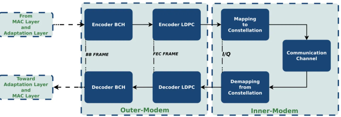
Chapter 1 — Introduction Outer-Modem Encoder BCH Encoder LDPC Mapping to Constellation Communication Channel Decoder BCH Decoder LDPC Demapping from Constellation
BB FRAME FEC FRAME I/Q
Inner-Modem From MAC Layer and Adaptation Layer Toward Adaptation Layer and MAC Layer
Figure 1-2 – General structure of the DVB-S2 standard.
noise ratio [97]. Finalized in 2004, the DVB-S2 [04] [05] standard was an evolution of the previous DVB-S standard. This new revision provides a better use of the spectral resources and a larger set of services through satellites. To improved the Quality of Services (QoS), DVB-S2 adopts an adaptive modulation and coding scheme. This scheme includes both Low Density Parity Check (LDPC) and Bose-Chaudhuri-Hocquenghem (BCH) channel coders with a near-to-1 coding ratio. Furthermore, DVB-S2 proposes a large panel of modulation schemes (QPSK, 8PSK, 16-APSK, 32-APSK). The choice of modulation and coding efficiency leads to a large range of spectral efficiency. In this section, we detail the structure and the computation requirements of the DVB-S2 transmission and reception chain.
The DVB-S2 standard is composed of a set of computation blocks (Fig. 1-2). Each block on the transmission line has its counterpart in the reception line. The computation involved in each block significantly differs and requires different hardware resources. In a general way, the transmitter involves less computation than the receiver.
BCH encoding: BCH codes form a large class of multiple random error-correcting binary codes.
They were first discovered by A. Hocquenghem in 1959 and independently by R. C. Bose and D. K. Ray-Chaudhuri in 1960. BCH codes are cyclic codes, i.e. multilevel, cyclic and variable-length error correction codes. These codes enable an accurate control of the error encoding and correction capacity. The BCH encoding phase could be easily done with a low consumption custom hardware component based on Linear Feedback Shift Register (LFSR) [AS15]. The decoding phase is based on a more complex linear algebra method called syndrome decoding.
LDPC encoding: LDPC codes were first introduced in 1962 by R.G. Gallager [Gal62]. Due to the
hardware limitations at that time, these codes could not actually be implemented. This was no longer true with the appearance of the iterative decoding process, and the LDPC were reintroduced in 1996 by D.J.C. Mackay [Mac99]. LDPC codes are linear block codes. They can be defined by a parity check matrix H of size M × N. The number of columns N in H represents the code length and the number of rows M represents the number of parity check functions that the code needs to satisfy. The density of non-zero elements in the H matrix is very low, and this is why they are called low density parity check codes. The encoding phase involved a series of binary Xor (⊕) operations applied on the transmission symbol with irregular patterns. LDPC decoding phase is based on the so-called message passing algorithms which are iterative algorithms such as the belief propagation algorithm. Their name derived from the fact that, at each round of the algorithm, messages are passed from message nodes to check nodes, and from check nodes back to message nodes. The messages from
Section 2 — Technology progress and architecture trends
message nodes to check nodes are computed based on the observed value of the message node and some messages passed from the neighboring check nodes to that message node. The LDPC decoding phase stays complex and requires a large amount of computation at each decoding iteration.
In a more general manner, the physical layer of radio transceivers could be divided into two main parts: the inner modem; and the outer modem. The inner modem includes environment param-eter estimation, data detection, and transmission. The outer modem performs the encoding and decoding of frames from the received/transmitted data stream. On top of those compute-intensive layers, a Multiple Access Control (MAC) layer could be necessary to ensure the timing and ac-knowledgment schemes. Those elements involve different signal processing tasks with their own duty cycle. For example, the inner modem is mainly composed of irregular computation schemes strongly connected to the targeted standard. On the other side, the outer modem involves more regular computation schemes and requires less flexibility. Furthermore, those computation blocks expose different types of parallelism (task-level, instruction-level, and data-level parallelism). To reach a good energy/performance ratio, it is more efficient to use the task level to split the applica-tion across multiple computaapplica-tion units, in order to independently tune each of these computaapplica-tion units (cf. Chapter 2 Section 3).
2
Technology progress and architecture trends
For the past three decades, Moore’s Law [Moo65] (roughly the doubling of on chip transistors every 18 months) has been a fundamental driver of the processor evolution. Coupled with the Den-nard scaling [Den+74], a series of circuit, architecture and compiler advances has emerged and led in exponential performance increase. Since the beginning of the century, processor designers have shifted from single-core processor performance increase to core count increase to fully exploit Moore’s Law scaling. Figure 1-3 depicts this phenomenon [BSW15]. The failure of Dennard scal-ing, partially addressed by the shift to Multi-processor System on Chip (MpSoC), may soon limit the multicore scaling just as single-core scaling has been curtailed. This leaves the community with no clear scaling path to exploit the still continuous transistor count increases. Lead by a new phenomenon called “Dark Silicon”, the integration of dedicated heterogeneous accelerators within microarchitecture begin to appear.
2.1
Towards the integration of dedicated HW accelerators
The failure of the Dennard scaling exposed through the limitation of the supply voltage scaling led to the “Dark silicon” issue [Esm+11]. In fact, the current transistor density and the limitation of transistor voltage scaling prevent the use of all the available transistors at the same time due to the overall power that could be dissipated by a chip. This is the physical factor that led to “Dark Silicon”. The percentage of a chip that can switch at full frequency drops exponentially with integration den-sity and thus energy efficiency is not scaling along with technology advances. Furthermore, this limitation can also come from the algorithm structure. Indeed, the available degree of parallelism within an algorithm is limited and thus cannot efficiently use a 100-core or even more a 1000-core chip. This parallelism limitation leads to the same issue: all available cores within a chip could not be used at the same time. Therefore, it could be interesting to use part of the available transistors to efficiently implement a dedicated task. These transistors will not be used all the time, but clearly improve performance when used. This phenomenon is highlighted through the integration of
spe-Chapter 1 — Introduction
Figure 1-3 – Processor microarchitecture and performance evolution [BSW15]. cialized on chip HW accelerators such as Application Specific Integrated Circuit (ASIC) or Field Programmable Gate Array (FPGA). This is the rise of Heterogeneous MpSoC (HMpSoC).
2.2
Energy efficiency: the next challenge of embedded systems
On top of this continuous research of performance improvement, a new key factor emerged: energy consumption. Indeed, with the democratization of embedded and wearable systems, that run on a limited power budget, energy consumption that directly impacts their autonomy is becoming a commercial issue. With their dedicated HW accelerators, the new class of HMpSoC architectures could address the challenge of energy efficiency. However, they introduce complex and hard-to-solve issues on SW/HW partitioning and task mapping. The high number of available cores and implementation types leads to a huge design space. Consequently, when energy consumption is a key requirement of the application, this solution space must be explored, early in the design phase, to obtain efficient solution. For this purpose, the overall design methodology needs to be revised to integrate fast and accurate power estimation tools. In the next section, we detail the different contributions that aim at addressing these objectives.
3
Contributions of the Thesis
This thesis proposes new methodologies and tools to address the complex task of energy-aware task mapping on HMpSoC architectures. For this purpose, we start by studying the properties and characteristics of different architecture structures that target the SDR field of application. Then, we look at the structure of multiple general purpose many-core architectures as well as heterogeneous
Section 4 — Organization of the document
architectures. These observations have allowed us to propose a generic definition of the target architecture family of this work alongside with a representation method.
Then, we propose a fast power modelling methodology for the HMpSoC architectures. This model focuses on the communications involved by the task mapping across the computational cores of the target architecture. We propose and validate an extraction method to use this power modelling methodology on real architectures.
This model is then used within a Design Space Exploration (DSE) method, based on a Mixed Integer-Linear Programming (MILP) formulation, which computes the best task mapping of tiled applications over a HMpSoC. The DSE method is coupled with an extraction method of the applica-tion/architecture characteristics that allows its use with other applications and architectures.
This modelling work highlighted the difficulties linked to the design and test of new energy-aware DSE. With this in mind, we present a HMpSoC emulation platform that embeds power mod-eling features and a representative test application framework. The obtained emulation platform enables the designer to simulate the behavior of application execution on a broad range of HMpSoC architectures in a reasonable time and open new perspectives for the design and test of energy aware DSE. This emulation platform was fully developed during this thesis.
4
Organization of the document
This thesis is organized as follows. The first part introduces the context of the work and pro-poses some related work pertaining to this thesis. Chapter 2 presents an overview of some dedi-cated SDR architectures alongside with general purpose many-core architectures. Thanks to these observations, we define the generic HMpSoC structure used in the following alongside with a rep-resentation method based on the communication channels. We also expose widespread application representation paradigms and precisely define the one used in the thesis work.
Chapter 3 presents a detailed state-of-the-art on multiple aspects of the work conducted during this thesis. Power modelling methods are presented at different levels of abstraction. Available meth-ods and tools for parallelism extraction are also detailed. The chapter ends with the introduction of current DSE methods.
The second part of the thesis details the contributions of this work. In Chapter 4, a communication-based power modelling tool is thoroughly presented. A description of the model structure is given alongside with a set of methods to use this model with real architectures. The methods and models are then used on a real architecture to validate this work.
This power modelling method is then used in Chapter 5 within a DSE tool that enables the mapping of tiled applications on a HMpSoC. This DSE tool proposes an energy-driven accelera-tor exploration for HMpSoC and enables the designer to select the optimal association of SW and HW computation block with the best processing distribution between the blocks. This method is validated on two application kernels on the Xilinx Zynq architecture.
Chapter 6 introduces an energy-aware HMpSoC emulation platform that enables to simulate the execution of a broad range of representative applications on various HMpSoC architectures. This chapter depicts the implementation structure of the emulation platform and the configuration fa-cilities. The execution models used and the corresponding execution framework are also depicted. Then, the method of application generation is presented as well as the automated application exe-cution mechanism through mapping directives.
Chapter 1 — Introduction Finally, Chapter 7 summarizes the contributions of this thesis and outlines the perspectives on future works.
Chapter
two
HETEROGENEOUS ARCHITECTURES:
STRUCTURES AND APPLICATIONS
Contents
1 Survey on MpSoC architectures . . . 19 1.1 Dedicated SDR architectures . . . 20 1.2 General Purpose architectures . . . 21 2 Generic HMpSoC representation . . . 25 2.1 Generic HMpSoC architecture . . . 25 2.2 Oriented tree for memory hierarchies . . . 26 3 Application structure and representation . . . 27 3.1 Parallelism-Level . . . 27 3.2 Data Flow programming models . . . 28 3.3 Control Flow programming models . . . 30 3.4 Mixed programming models . . . 30 4 Generic application structure . . . 32
In the first section of this chapter, some architectures dedicated to SDR are depicted. A highlight is given on the heterogeneous part introduced to answer the computation challenges involved by the communication chain. In addition, we present general purpose MpSoC with potential hetero-geneous features and show how we could draw performance from them in the SDR context. Then, we propose in Section 2 a generic definition of heterogeneous many-core architecture alongside with a generic description model used in the following works. In Section 3 we introduce structures and representations employed to model applications. Finally in Section 4, we conclude with the representation of the application that we use in this work.
1
Survey on MpSoC architectures
The introduction highlighted that the use of heterogeneous multi-core architectures can enhance the power efficiency of the solution. In the following, we detail how heterogeneity was introduced within MpSoC architectures. We particularly focus on architectures dedicated to SDR applications. Then, we present some general-purpose architectures and how SDR applications could draw benefits from them.
Section 1 — Survey on MpSoC architectures Core 3 iCache SBX Memory SHB Core 2 iCacheSBX Memory SHB IO and Other Interfaces IO and Other Interfaces IO and Other Interfaces Core 1 iCache SBX Memory SHB HSN 4 AMBA ARM IO Subsystem Memory Subsystem DMA Device Controller Buses HSN SBX Complex
Figure 2-1 – Sandbridge SB3500 platform architecture [Pal+10].
1.1
Dedicated SDR architectures
This section presents an overview of the available SDR architectures that embed both HW and SW cores. Their general structures are depicted with a focus on their heterogeneity. More details could be found in the survey on SDR platforms proposed by Palkovic et al. [Pal+10].
Sandbridge SB3500 [Nac08]: The SDR platform SB3500 from Sandbridge is composed of four
processor cores. The control and platform management tasks are performed by one ARM proces-sor (Fig. 2-1. The inner- and outer-modem computation tasks are performed by three custom SIMD sandblaster cores developed by Sanbbridge. This platform proposes a limited amount of heterogene-ity through the use of two kinds of processor architecture.
Infineon Music [Ram07]: The Music platform (Fig.2-2a) from Infineon gathers four SIMD cores
with various accelerators such as FIR filter and turbo/viterbi accelerators. The SIMD cores cou-pled with the filter accelerators are dedicated to the inner-modem computation. The outer-modem treatments are implemented mainly within the turbo/viterbi accelerators.
ARDBEG Platform [Woh+08]: A collaboration between ARM and the University of Michigan
led to the ARDBEG platform (Fig.2-2b). This platform is composed of three SIMD processors, one dedicated to control and the two others dedicated to inner-modem treatments. The outer-modem computation is performed with the help of a hardware turbo accelerators.
IMEC’S BEAR Platform [Bou+08]: The Base band Engine for Adaptive Radio (BEAR),
devel-oped by IMEC, is a heterogeneous multi-core architecture (Fig.2-3) composed of six processor cores coupled with two hardware accelerators. The six processors consist of one general purpose ARM processor dedicated to control and MAC layer, three Application Specific Instruction Processors
Chapter 2 — Heterogeneous Architectures: Structures and Applications Multilayer Bus SIMD Core 1 40K Memory SIMD Core 2 40K Memory SIMD Core 3 40K Memory SIMD Core 4 40K Memory SIMD Core Cluster
Bus Bridge Shared Memory FIR Accelerator Rf Interfaces External
Mem I/FExternalMem I/F Turbo/ViterbiAccelerator
(a) Infineon MuSIC-1 platform architecture [Pal+10]
Peripherals DMAC CoprocessorTurbo
L1 Mem Execution Unit Control Processor L1 Mem L2 Memory Execution Unit L1 Mem L1 Data Mem L1 Program Mem 1,024-b SIMD RF 512-b SIMD RF Pred RF Scalar RF AGU RF Interconnect 512-b SIMD Mult 512-b SIMD ALU 512-b SIMD Shuffer Scalar-SIMD Transform Unit Scalar ALU AGUs Interconnect Ardbeg System Ardbeg PE
(b) ARM/University of Michigan’s Ardbeg architecture [Pal+10]
Figure 2-2 – Architectures with dedicated FEC accelerators.
(ASIP) dedicated to coarse time synchronization (DFE processing block), and two architectures for dynamically reconfigurable embedded systems (ADRES) dedicated to inner modem computation. The ASIPs are built around a 5-way VLIW with two scalar and three vector computation lines. The ADRES cores are highly flexible and energy efficient Coarse Grain Reconfigurable Architectures (CGRA). Finally, two hardware accelerators dedicated to Viterbi decoding are added. All those ele-ments are connected through Advanced Micro-controller Bus Architecture (AMBA).
The four architectures presented consist of mainly two approaches. On the one hand, architec-tures such as Sanbbridge SB3500 (Fig. 2-2a) focus on reconfigurability at a cost of a low hetero-geneity with no use of dedicated hardware accelerators. This approach enables to address a wide range of communication standard at the cost of energy-efficiency and performance. Platform such as Infineon Music and ARDBEG are more mitigated (Fig. 2-2). They use the heterogeneity by using dedicated FEC hardware accelerators, which improves performance and energy-efficiency but nar-rows the spectrum of targeted standard. On the other hand, the BEAR platform (Fig. 2-3) focuses on heterogeneity with a large panel of dedicated accelerators such as domain-specific reconfigurable accelerators and dedicated FEC accelerators. The obtained performance per watt is high, but the use of dedicated FEC components introduces the same issues as before. Furthermore, if we focus on the aspect of cost and time-to-market, the development of a new architecture for each new kind of communication standard is not really efficient.
1.2
General Purpose architectures
In this section, we briefly present some general-purpose MpSoC architectures. As those archi-tectures are not necessarily heterogeneous, we proposed some solutions or suggestions to introduce reconfigurable hardware components in them.
Network on Chip With the scaling of microchip technologies, the number of heterogeneous
com-putation units integrated within a single chip has exploded. The communications between those ele-ments encounter fundamental physical limitations such as time-of-flight of electrical signals, power
Section 1 — Survey on MpSoC architectures ARM9 Cell ITCM Boot RAM SPI Host IO Host Interface DTCM Clock and Power Management Test Interface L2 RAM Interrupt ctrl GPIO Timers APB Bridge APB Two-Layer AHB
DMA1 DMA2 DFEAHB
Interface DCO Comp I Buffer DCO Comp Q Buffer DFE Tile ctrl Detect Engine IMEM DMEM IMEM DMEM I Buffer Q Buffer Front-End Interface ADRES Core L1 bk0 ADRES AHB Interface ADRES I$ ADRES IMEM L1 bk1 bk2L1 bk3L1 FEC AHB Interface FIFO
FIFO ViterbiDecode Descrambl CRC CRC Scrambl Conv Encode FIFO FIFO FEC Accelators DFE ARM Subsystem Baseband Engines
Figure 2-3 – IMEC’s BEAR SDR platform [Pal+10].
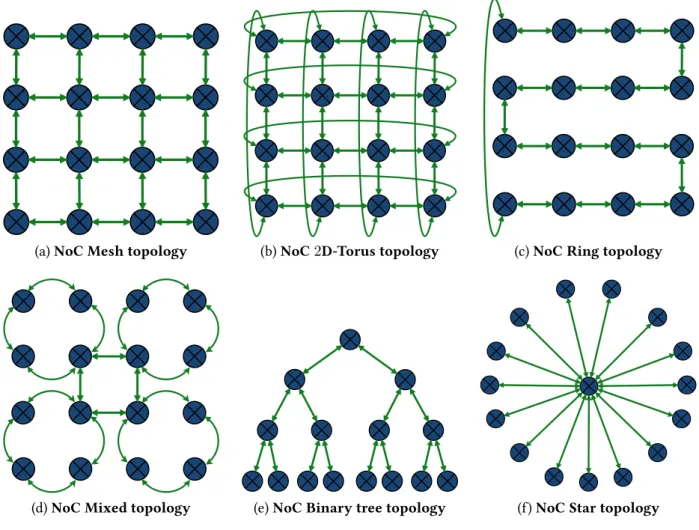
use in driving long wires/cables, etc. The well understood concepts of bus communications intro-duce numerous drawbacks that prevent the scaling of these technologies within the many-era. In fact, every new units added on a communication bus introduce a parasite capacitance that degrades the electrical performance of the wires. Once the communication between two entity was estab-lished the latency is wire-speed, nevertheless the bandwidth is limited and shared between all the units. Then, with the multiplication of the master units on the bus, the arbitration delay grows and becomes a bottleneck. To overcome theses issues and get a scalable communication infrastructure, the concept of Network on Chip (NoC) was introduced. With this approach, for all network sizes, only point-to-point one-way wires are used, thus local performance is not degraded when scaling. The routing decision could be well distributed if the network protocol used is non-central. The over-all aggregated bandwidth scales with the network size, nonetheless the internal network contention may cause latency and degrade the performance.
The NoC latency depends on the physical characteristics of the hardware implementations, the distance between two units expressed in number of hopes within the network and the network con-tention. The two last elements are strongly connected with the application communication pattern and with the network topology. Fig. 2-4 shows a panel of the most widespread NoC topologies. The used topology influences the average number of communication hopes and the network congestion. For example, Fig. 2-4c shows a ring topology which is simple to manage and arbitrate. As a counter-part, this topology presents a high number of average hopes and it is very sensitive to congestion. The mesh topology (cf. Fig. 2-4a) lowers the average number of hopes but the traffic could be eas-ily saturated in the middle of the NoC. The 2D-torus topology solves this issue, but requires more area on the chip. The choice of the target topology is hard and its efficiency is tightly linked to the application communication pattern.
Chapter 2 — Heterogeneous Architectures: Structures and Applications
(a) NoC Mesh topology (b) NoC 2D-Torus topology (c) NoC Ring topology
(d) NoC Mixed topology (e) NoC Binary tree topology (f) NoC Star topology
Figure 2-4 – Panel of common NoC topology.
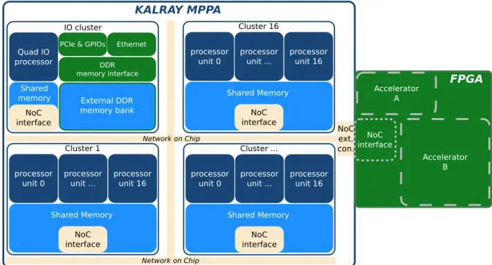
Kalray MPPA: Kalray’s Massively Parallel Processor Array (MPPA) architecture [Din+13] is a
homogeneous MpSoC which is mainly composed of 256 VLIW processors gathered into 16 clusters. All clusters are linked together through two NoCs, one with low bandwidth for control information and one with high-bandwidth for data communications. External communications are managed through four I/O clusters. Figure 2-5 shows a simplified block diagram of a MPPA-256 processor chip. Each cluster contains 16 5-way VLIW processors and NoC interface. On each side of the cluster array, an I/O cluster provides access to external Double Data Rate (DDR) memory banks and to PCIe and Ethernet interfaces. The use of power-efficient VLIW computational cores alongside with the homogeneous and widely parallel architecture enables an efficient 50 GFLOPS/Watts ratio for the first version and forecasts to meet a ratio up to 100 for the third one. Furthermore, the design of the embedded NoC enables its access directly through the IO as an external cluster. This opens the way for heterogeneous computing by connecting an external reconfigurable accelerator such as FPGA that can directly communicate with the NoC.
Mellanox TILE-Gx: The TILE-Gx architecture [Mel] includes an array from 36 up to 72 tiles
(cores). Each tile is built around a 64-bit 3-way VLIW processor, integrating three levels of cache, and a non-blocking switch that integrates the tile into a power-efficient interconnect mesh. The TILE-Gx architecture offers 23.5 MB of on-chip cache with the Mellanox’s (formerly Tilera) dynamic distributed cache technology that provides a 2× average improvement in cache coherence perfor-mance over traditional cache coherence protocol. Each tile can independently run a complete OS or multiple tiles can be grouped together to run a multi-processing OS like Symmetric Multi-Processor (SMP) Linux. A dynamic power management unit enables the tiles to be put into a low-power sleep
Section 1 — Survey on MpSoC architectures
Network on Chip
Network on Chip
PCIe & GPIOs
Quad IO processor processor unit 4 Shared memory NoC interface Ethernet DDR memory interface External DDR memory bank IO cluster processor unit ... processor unit 0 processor unit 16 Shared Memory NoC interface Cluster 16 processor unit ... processor unit 0 processor unit 16 Shared Memory NoC interface Cluster ... processor unit ... processor unit 0 processor unit 16 Shared Memory NoC interface Cluster 1 NoC ext. con. Accelerator A Accelerator B NoC interface FPGA KALRAY MPPA
Figure 2-5 – Kalray’s MPPA architecture extended to heterogeneous.
mode independently and achieved a ratio close to 25% GFLOPS/Watts. This architecture can be extended by connecting multiple chips through a shared DDR memory or Ethernet interfaces. In-cluding hardware accelerators, such as some FPGA, establishes heterogeneous architecture.
Xilinx Zynq: The Zynq architecture from Xilinx [Cro+14] is representative of heterogeneous
targets as it combines two ARM cortex A9 processors with an FPGA fabric (see Fig. 2-7). The Zynq computation cores communicate through different memory levels: L2 cache and DDR. Each level can be accessed from two channels: one for SW and one for HW. Furthermore, synchronization and configuration communications can occur from a dedicated channel without memory bank access. This enables low-latency communications with zero-copy approach. The low-power processor cores and the dedicated reconfigurable accelerators coupled with the low-latency communication scheme enable to address a wide range of embedded applications with good energy-efficiency.
As shown in Sub-Section 2.1 the actual architectural trend and the new dark silicon paradigm led to the multiplication of the computational cores and to the integration of heterogeneous accelera-tors. The NoC communication scheme, that is now used inside SoC, enables the scalability of the architecture and leads to a new paradigm of core simplification combined with their multiplication, which enhances the computational power per Watts. This section presents multiple approaches to take advantage of these elements. The first option was to start building dedicated architecture but this solution reduces the scope of the produced chips and increased their cost. The second solution was to add reconfigurable accelerators inside general purpose architectures. The reconfigurabil-ity of the accelerators coupled with the computational power of the high number of cores and the communication flexibility given by the NoC enable to target a wide number of applications with effi-ciency on the same architecture. This approach opens up wide opportunities at the cost of hardening the application development. In fact, with those highly parallel and configurable architectures, the slightest choice on application implementation could have a strong effect on energy consumption and performance. The design space of those architectures is wide, but its full exploration is more essential than ever.
![Figure 1-3 – Processor microarchitecture and performance evolution [BSW15].](https://thumb-eu.123doks.com/thumbv2/123doknet/11509624.294076/24.892.87.810.78.548/figure-processor-microarchitecture-performance-evolution-bsw.webp)
![Figure 2-1 – Sandbridge SB3500 platform architecture [Pal+10].](https://thumb-eu.123doks.com/thumbv2/123doknet/11509624.294076/29.892.196.697.82.483/figure-sandbridge-sb-platform-architecture-pal.webp)
![Figure 2-3 – IMEC’s BEAR SDR platform [Pal+10].](https://thumb-eu.123doks.com/thumbv2/123doknet/11509624.294076/31.892.198.699.83.545/figure-imec-s-bear-sdr-platform-pal.webp)
![Figure 3-2 – General structure of genetic algorithms [Cor14].](https://thumb-eu.123doks.com/thumbv2/123doknet/11509624.294076/51.892.86.791.101.388/figure-general-structure-genetic-algorithms-cor.webp)
