TH `ESE
TH `ESE
En vue de l’obtention du
DOCTORAT DE L’UNIVERSIT´E DE TOULOUSE
D´elivr´e par : l’Universit´e Toulouse 3 Paul Sabatier (UT3 Paul Sabatier)Pr´esent´ee et soutenue le 09/10/2018 par : Daya Sagar DHUNGANA
Growth of InAs and Bi1-xSbx Nanowires on Silicon for Nanoelectronics and Topological Qubits by Molecular Beam Epitaxy
JURY
M. Filadelfo CRISTIANO Directeur de
Recherche,LAAS-CNRS, Toulouse
Pr´esident du Jury M. Erik P.A.M. BAKKERS Professeur d’Universit´e, TU
Eindhoven, Eindhoven, The Netherlands
Rapporteur
M. Aristide LEMAITRE Directeur de
Recherche,C2N-CNRS, Marcoussis
Rapporteur Mme Yamina ANDRE Maitre de Conference,Institut
Pascal - UMR 6602,Clermont-Ferrand
Examinateur
´Ecole doctorale et sp´ecialit´e :
GEET : Micro et Nanosyst`emes
Unit´e de Recherche :
LAAS-CNRS (UPR 8001)
Directeur de Th`ese :
S´ebastien PLISSARD
Rapporteurs :
war which opens the door to heaven. Stand up and perform your duty and,
therefore, fight with peace in thy soul.”
“A Karma-yogi should fight while treating victory and defeat alike, gain
and loss alike, pain and pleasure alike and fighting thus, he does not incur
sin”
“You have the right to work, but never to the fruit of work. You should
never engage in action for the sake of reward, nor should you long for
inaction.”
“Perform work in this world, Arjuna, as a man established within
him-self – without him-selfish attachments, and alike in success and defeat.”
Source (Srimad Bhagavat Gita)
Parents
Brother and Sister
Future Wife !
First and foremost, I want to express my heartfelt gratitude, great respect, and sincere thanks to my supervisor, Dr. Sebastien Plissard for his constant and continuous support, guidance and encourage-ments throughout this thesis. The confidence, motivation, passion, performance and outcomes that I have now in front of me are the direct consequences of the total autonomy that I benefited during the thesis. The work would not have reached this level without his valuable inputs, encouragements and willingness to spare so much time. I also thank him for the detailed reviews, useful comments, and corrections when reviewing my papers, thesis manuscript, and slides that helped me to improve myself each time. I also thanks him for his timely advises as well as willingness to discuss whenever needed. It has been a real pleasure working with him.
I would also like to thanks the jury members for their kindness for participating to my Ph.D. defense and for their valuable questions and concerns about my work. Many thanks to Prof. Dr. Erik P.A.M. Bakkers and Dr. Aristide Lamitre for earnestly reading the thesis and their valuable remarks, and to Dr. Filadelfo Cristiano and Prof. Dr. Yamina Andre and for investing their precious time on playing the role of the president of jury and the thesis examiner respectively.
I am grateful to Dr. Alexandre Arnoult for helping me in gaining confidence with the MBE system in a relatively short time. I thank him sincerely for his help and professionalism, for teaching me things that will be useful perhaps throughout my career. I also appreciate and thank Guy Lacoste and Quentin Gravelier for their help in day to day technical stuffs. My special thanks are due to Benjamin Reig and Jean Baptiste for training me the Scanning Electron Microscopy and chemical security respectively. I am also grateful to Dr Guielhem Larrieu and my friend Nicolas Mallet for providing me the patterned Silicon wafers. Also, thanks to Dr. Fuccio Cristiano, Dr. Pier Franchesco and PhD. student Ragada Makaram for the assistance in TEM characterizations. I am grateful to Dr. Anne-Hemeryck for her time on assisting us on DFT simulations. It was quite an amazing experience.
I have received tremendous help and support from the administrative staffs from the univesity and LAAS-CNRS throughout my Ph.D. It would like to thank them a lot. It would have been impos-sible to manage my way through the subtleties of the French bureaucracy and tedious administrative issues without their help. I thank Anais for being always-ready-to-help, for her assistance and help in preparing missions and in smooth organization of activities related to the defense. I also thank Katia and Yasmine from the Paul Sabatier university for their prompt administrative help. I thank Marie Estruga, Somdel Diaham and Alan Cazzare for their help related to the doctoral school. I especially
thank Catherine Stasiulis for the clean and smooth progress with the prefecture administration. I have been very fortunate to be part of the MPN team, a very dynamic and supportive team in understanding the students matters and their personal developments. Guilhem Larrieu, Filadelfo Cristiano, Eléna Bedel-Pereira and Emmanuel Scheild, thanks for your encouragements during these three years. Also thanks to my colleagues: Léa Farouil and Richard Monflier for sharing the same office and helping me in difficult french to easy french translations. Special thanks to Clara Cornille for some good times in the clean room. I would also like to thank Nicolo Sartori and Hugo Lacombe for assisting me in the project during their internships.
I am also grateful to all the people whom I meet and share nice moments during this thesis. My special thanks go to Suman Bista for his encouragements and some of the fruitful discussions on ’Doctor of Philosopy stuffs’. I am thankful to the classmates from my engineering school; Sandesh, Suraj, Shusil, Shiva, Bibek Jung, Paribesh, Bibek Joshi, Ayush, Amit, Gajendra Jung, Drona Raj, Swatantra, Sandeep etc. ... for good times that we had during our undergraduate and especially the football matches between two groups of the same class. Additional thanks to Gajendra, Drona, my sister Richa and Anusha for making my trip to Boston as one of the unforgettable trip so far I had. My peer-mates, Sohan and Bishnu for their constant inspirations. I am grateful to my friends from Indian subcontinent. First and foremost thanks to Magdhi and her familiy for encouraging me to bring full potential outside. Nikhil, Sid and Simul thanks for your help during the master days. Dheeraj Kumar and Abhishek Kumar for their supports in LAAS-CNRS. Thanks to the Nepalese in Toulouse and Clermont-Ferrand for some of the exciting times during Nepalese festivals; Sudeep and Ankita, Salona, Sri-Jan , Roshan ; thanks a lot. Also thanks to my landlord Christophe and his kids Philemon and Eliot for making the stay in Toulouse smooth.
Finally and above all, my deepest gratitude goes to my family for their constant inspiration, support, and encouragements. I am blessed to have those parents who always ranked education in their highest priority and have faith in me, a brother who always stands on my side and a very courageous sister. It’s thank to your love, blessings, and selfless sacrifices, despite being physically separated, that all my successes and achievements have been possible.
0 General Introduction 1 1 Nanowires and Applications 5
1.1 Nanoelectronics . . . 8
1.2 Spintronics . . . 9
1.3 Phase Change Memories . . . 10
1.4 Piezoelectrics . . . 11
1.5 Optoelectronics . . . 13
1.6 Solar Cells . . . 14
1.7 Water Splitting and H2Generation . . . 15
1.8 Li-Ion Battery . . . 17
1.9 Thermoelectrics . . . 18
1.10 Sensors . . . 20
2 Tools and Methodologies 23 2.1 The Molecular Beam Epitaxy . . . 23
2.1.1 The cluster . . . 24
2.1.2 The loading chamber . . . 25
2.1.3 The preparation chamber . . . 25
2.1.4 The growth chamber . . . 26
2.2 The electron microscopy . . . 28
2.2.1 The scanning electron microscope . . . 29
2.2.2 The transmission electron microscope . . . 30
2.3 The X-Ray diffraction . . . 31
2.4 The statistical analysis of nanowires . . . 33
2.4.1 The image processing . . . 33
2.4.2 Data Analysis . . . 34
3 The Nanowires Growth Mechanisms 37 3.1 The VLS growth mode . . . 38
3.1.1 Thermodynamic Considerations . . . 40
3.1.1.1 Gibbs-Thomson Effect . . . 40 vii
CONTENTS
3.1.1.2 Nucleation from Molten Metal Alloy Droplet . . . 45
3.2 The VS Growth Mode . . . 46
3.3 The Crystalline Structure . . . 47
3.4 The Density Functional Theory . . . 48
4 Nanoelectronics with InAs Nanowires 53 4.1 The Classical Electronics . . . 54
4.1.1 The Bipolar Junction Transistor (BJT) . . . 54
4.1.2 The Field Effect Transistor (FET) . . . 54
4.1.3 The Complementary Metal Oxide Semi-Conductor (CMOS) . . . 55
4.1.3.1 The Constant Field Scaling . . . 56
4.1.3.2 The Constant Voltage Scaling . . . 57
4.2 The Short Channel Effects . . . 57
4.3 The semi-classical Electronics . . . 58
4.3.1 The High-K Dielectrics . . . 58
4.3.2 The Metallic Gates . . . 59
4.3.3 The Strain Engineering . . . 59
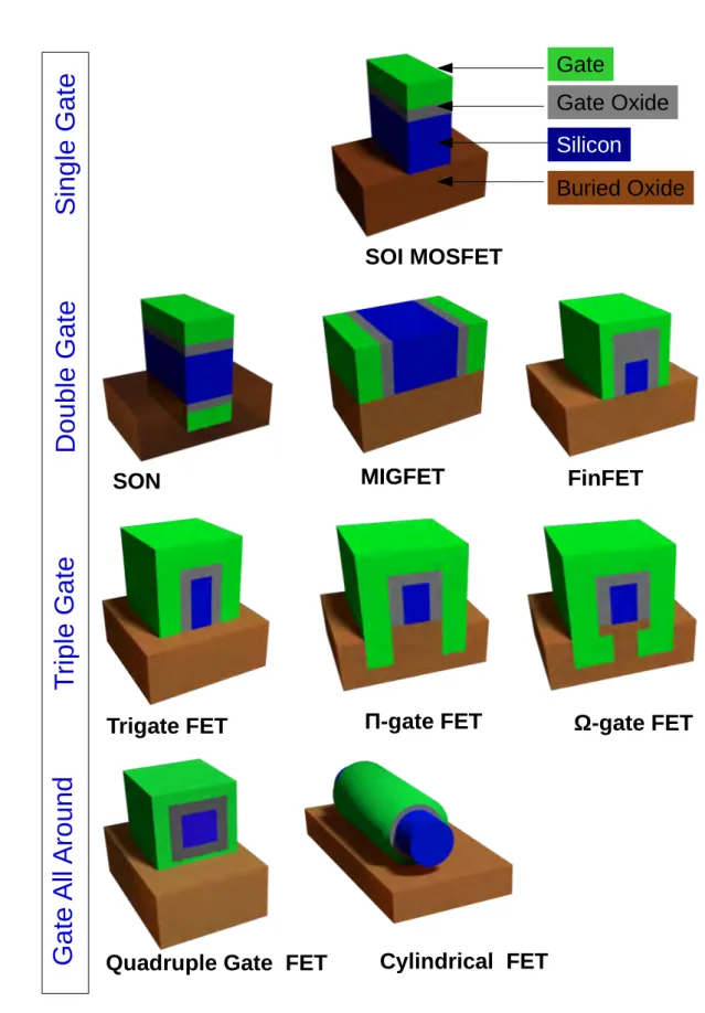
4.3.4 The Silicon On Insulator and the Multi Gate Architectures . . . 60
4.3.4.1 Physics Behind multi gate architectures . . . 61
4.4 The High Mobility Nanowires . . . 64
4.5 My Contribution . . . 66
4.5.1 The Initial Growths . . . 66
4.5.1.1 The Experimental Description . . . 66
4.5.1.2 Influence of the degassing temperature during Hydrogen treat-ment . . . 67
4.5.1.3 Influence of the amount of Hydrogen . . . 68
4.5.1.4 Influence of the Arsenic Treatment Temperature . . . 69
4.5.2 Full CMOS Compatible InAs Nanowires . . . 70
4.5.2.1 The Experimental Description . . . 70
4.5.2.2 The SEM Analysis: influence of the surface preparation on nanowire growth . . . 70
4.5.2.3 The Statistical Analysis of the Nanowires Morphology . . . 73
4.5.2.4 The TEM Analysis . . . 78
4.5.2.5 AFM Measurements of the Surface Roughness . . . 81
4.5.3 The DFT Analysis . . . 82
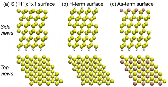
4.5.3.1 Details on DFT Calculations . . . 82
4.5.3.2 Considered Surfaces for DFT Calculations . . . 83
4.5.3.3 Adsorption reaction and energy . . . 83
4.6 Conclusion . . . 90
5 Bi1-xSbxNanoscale 3D Topological Insulators for Quantum Computing 93 5.1 The Qubits . . . 94
5.2 Materials for Qubit implementation . . . 95
5.3 Topological qubits in 1D hybrid systems . . . 97
5.4 3D Topolgical insulators . . . 98 5.4.1 The TI Nanostructures . . . 100 5.5 The Bi1-xSbxalloys . . . 101 5.6 My Contribution . . . 102 5.6.1 First growths . . . 102 5.6.1.1 First nanostructures . . . 103 5.6.1.2 Nanoscale Geometry . . . 104 5.6.1.3 Structural Characterizations . . . 105
5.6.2 Control of Sb compostion in Bi1-xSbxnanostructures . . . 109
5.6.3 XRD of Growth Matrix . . . 113
5.6.3.1 The Powder Diffraction measurement . . . 113
5.6.3.2 The XRD Results . . . 114
5.6.3.3 Analysis of the XRD measurements . . . 115
5.6.4 Advanced characterizations . . . 118
5.7 Conclusions and outlooks . . . 119
AC Alternating Current BEP Beam Equivalent Pressure BJT Bipolar Junction Transistor
CMOS Complementary Metal Oxide Semiconductor CPU Central Processing Unit
DFT Density Functional Theory
DRAM Dynamic Random Access Memory ENG Equivalent Number of Gates FET Field Effect Transistor FIB Focused Ion Beam
FTJ Ferroelectric Tunnel Junction GMR Giant Magetoresistance IC Integrated Circuit
ITRS International Technology Roadmap for Semiconductor LASER Light Amplification by Stimulated Emission of Radiation LED Light Emitting Diode
MAF Mass Air Flow
MBE Molecular Beam Epitaxy MOS Metal Oxide Semiconductor
MOSFET Metal-Oxide-Semiconductor Field-Effect Transistor MOVPE Metal Organic Vapor Phase Epitaxy
MQWs Multiple Quantum Well MTJ Magnetic Tunneling Junction NVM Non Volatile Memory
CONTENTS PEC Photoelectric Cells
PID Proportional–Integral–Derivative
PRAM Programmable Random Access Memory QDs Quantum Dots
QWs Quantum Wells RF Radio Frequency S/V surface-to-volume SAE Selective Area Epitaxy
SAED Selected Area Electron Diffraction SEM Scanning Electron Microscopy SNR Signal to Noise Ratio
SOI Spin Orbit Interaction
STT-RAM Spin Transfer Torque Tunneling Random Access Memory TCO Transparent Conductive Oxide
TEM Transmission Electron Microscopy TFET Tunneling Field Effect Transistor TFNG Transparent and Flexible Nanogenerator TI Topological Insulator
TRS Time Reversal Symmetry UHV Ultra-High Vacuum UV Ultra Violet
VLS Vapor-Solid-Liquid VS Vapor-Solid
General Introduction
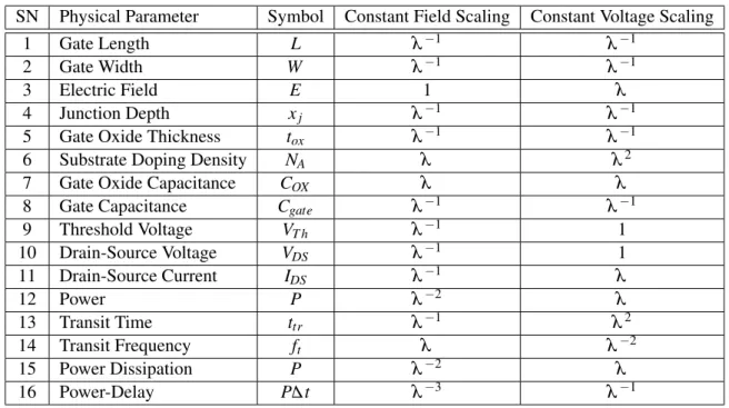
In the middle of the 1960s, Gordon Moore, the co-founder of Intel, proposed a law to estimate the evolution of the electronic field: the number of transistors per square inch should double in every two years. The most astonishing point about this prediction is that it remained very accurate for many decades and even drives the nanoelectronics field nowadays. The manufacturing processes progressed from the 50 μm node in the mid 1960s to the 90 nm in 2003, however, the industry faced major bottlenecks to go beyond 90 nm node as short channel effects and quantum mechanical effects araised in the transistors due to miniaturization. In order to address these limitations, the industry focused efforts on material engineering and device architecture. For instance, HfO2 was
adopted to replace the SiO2due to its high dielectric constant, the metallic gates were chosen rather
than poly-Si gates gates in order to avoid the gate leakage currents and strained silicon was also used in devices to boost the mobility. Furthermore, in 2011, the industry embraced the multi-gate architecture (FinFET) to ensure better gate control over the channel. As it can be seen, the industry worked a lot on new materials to fit the Moore’s law up to the 7 nm node (A12 bionic chip from Apple) in 2018.
However, it is unlikely for standard technologies to reach beyond the 5 nm technology node, which led to the concept of Beyond-Moore: a different way of continuing Moore’s law beyond scal-ing limits of current Si technology by either changscal-ing material or architecture. In this context, the vertical integration of nanowires on silicon solves some of those fundamental issues. For instance, the vertical integration allows to use nanowires as channel to build 3D Gate-All-Around (GAA) transistors, which is to the date the most optimized configuration. On the other hand, the integration of III-V nanowires on silicon in the last two decades witnessed significant advancements. Hence, its not surprising that, they are regarded as a possible building block for future transistors as reported in the last International Technology Roadmap for Semiconductors (ITRS).
In addition, it is worth mentioning that some key applications need extremely high computa-tional power. The most common example is the modern cryptography which relies on the factor-ization of very large prime numbers which would be efficiently tackled with new computational approaches based on Qubits and Quantum Computers. The advantages of Qubits is that they rely on a two state quantum mechanical system that can be ’0’ or ’1’ or ’both’ at the same time
trary to standard bits. Because of this property, the quantum computers show exponential gain in processing time with the number of Qubits. For these reasons, the scientific community put high ef-forts on building Qubits in new materials. In this context, many candidates were studied: Josephson Junctions, spin defined qubits in quantum dots, defects in solids, hyperfine states in ion trapped sys-tem syssys-tem and Majorna Fermions in a semiconductor nanowire hybrid interface. The fundamental requirements for “good” qubits are: long coherence time, insensitive to the external noise and error-free. In this context, Majorana fermions (MFs) can be used to implement topological qubits and can be engineered in a nanowire having Spin Orbit Interactions (SOIs).
In the quest of Mfs, a group from TU Delft led by Prof Leo Kouwenhoven reported the first signatures of Mfs at two ends of a InSb nanowire. In their recipe for building Mfs, the key ingre-dients are: (i) a nanowire, (ii) high SOIs, (iii) a superconductor and (iv) a magnetic field. Since the nanowire material (InSb) is a semiconductor, the first step is to induce superconductivity by proximity effect. Since the SOIs are large in InSb, the external magnetic field allows the creation of topologically protected states at the superconductor/semiconductor interface; and MFs can appear as zero energy modes. From the material point of view, replacing the InSb nanowires by new nanoscale 3D Topological Insulators (3DTIs) could be interesting. Indeed, 3DTIs are a new family of materials that are conducting at their surface and isolating in the core. They were first theoretically predicted a decade ago in 2007 by Fu and Kane from University of Pennsylvania, and measured experimentally one year later by a group of scientists led by Prof. Zahid Hasan from Princeton University.
In the context of high electrons mobility transistors and topological qubits, this thesis aims at developing new materials that are suitable for these applications. The materials we developed are nanowires based on InAs and Bi1-xSb. The high mobility of InAs is interesting for nanoelectronics
and similarly the 3D topological behavior of Bi1-xSbxcan be used in the realization of Mfs based
Qubit devices. In both cases, the primary objective is to improve the quality of the nanoscale mate-rials while addressing some of the key technological bottlenecks. In this thesis work, we study and demonstrate full CMOS compatible InAs nanowire integration on Si by Molecular Beam Epitaxy (MBE), and the growth of Bi1-xSbxnanowires on Si with controlled composition.
The architecture of the thesis is the following:
The Chapter 1
presents the nanowire research field from the materials to the applications. First, a few key historical moments are reported briefly and followed by a discussion on different possible geometries that emerged along with the progress in nanowires growth. Finally, 10 key applications are proposed and for each of them the advantages of the nanowire geometry are listed.The Chapter 2
presents the tools and technologies we used for nanowire growth, character-ization and the analysis method. The chapter starts with a brief description of a standard Molecular Beam Epitaxy (MBE) system followed with a brief introduction to Scanning Electron Mircrosopy (SEM) and Transmission Electron Microscopy(TEM). Similarly, the X-Ray Diffraction (XRD) mea-surement is discussed briefly. At the end, the image processing steps and the data treatment proce-dures, that were developed using standard open source tools are presented. This semi-automatic image processing and fully automatic data analysis facilitated the statistical analysis of nanowiresThe Chapter 3
provides an overview of the nanowire growth and the nucleation processes. First the Vapor-Liquid-Solid (VLS) growth mechanism and the thermodynamic and kinetic aspects during nucleation are discussed. Next, the Vapor-Solid (VS) growth mechanism is presented, as well as, the two possible crystalline structures: Zinc Blende (ZB) and Wurzite (WZ). Finally, the Density Function Theory (DFT) is briefly explained.The Chapter 4
deals with the integration of InAs nanowires on Silicon for high mobility nanoelectronics. In this chapter, first a brief introduction of the electronics technologies is presented. This includes a historical description, the scaling laws, the issues with the 90 node technology and the necessity of new nanoscale materials. Next , the state of the art is presented before we focus on our contribution where we report first the advantage of an hydrogen treatment. Next, a full CMOS compatible process that even addresses the Back-End-of-Line (BEOL) thermal limit is presented leading to fully CMOS compatible InAs nanowires on silicon. In the later part, a full growth study on patterns in Silicon is presented leading to the integration of InAs and InAsSb nanowires. The chapter also enlightens a change in the growth mode from VS to VLS. Finally DFT simulations are developed to qualitatively characterize the surface treatment.The Chapter 5
deals with the integration of Bi1-xSbxnanowires on Si with a controlled Sbcomposition. The chapter starts with the brief introduction to quantum computing, to the mate-rial aspects of quantum computing and to the topological qubits. Following, 3D topological ma-terials are presented, before we report our contribution to the field. First the initial growths of Bi1-xSbxnanowires are presented, allowing good control of the Sb. In parallel, a full investigation
of the influence of Bi, Sb and the growth temperature is presented, leading to different nanoscale geometries. In addition, a complete TEM characterization of the Bi1-xSbxnanowires is carried out
showing defect free single crystalline nanostructures having 3 kind of facets. Finally EDS-TEM and XRD compositions are compared showing good agreements, and low Sb composition compatible with the TI region are achieved.
Nanowires and Applications
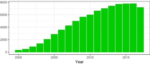
The history of nanowires dates back to 1964 when Wagner and Ellis from the Bell Telephone Lab-oratory used the Vapor-Liquid-Solid (VLS) mechanism to grow single crystalline Si nanowhiskers1. It was however only in the mid-1990s that the group of Prof. K. Hiruma, from Hitachi in Japan, synthesized the first III-V nano whiskers2–4 including a PN junction5. Thanks to the reduction of their diameter in the following years, they were finally renamed “nanowires”. At the beginning of the 21stcentury, and due to their unique geometry, nanowires gathered an immense research interest and are at present one of the most explored topic. The bar plot in 1.1 repensents the evolution of the field since 2000 and further highlights the attentions that nanowires received recently.
Figure 1:Publications with keyword “nanowires” since 2000.
Source Web of Knowledge
Figure 1.1 – Number of Publications recorded with the keyword “nanowires” (y-axis) since 2000 for each years (x-axis) . Source: Web of Science (http://apps.webofknowledge.com/)
Nanowires are 1D nanostructures, whose diameter is measured in few tens of nanometers(nm) and length in few microns(µm). Consequently, their surface-to-volume ratio (S/V) is high compared to their 2D counterparts. Additionally, this 1D geometry can withstand high strain and fabrication of defect free structures with high crystalline quality is possible. Thus, one can engineer the materials’ intrinsic properties at nanoscale including electrical, optical and magnetic properties; making them ideal candidates for the development of new nanoscale devices in the fields of nanoelectronics,
optoelectronics, memories, energy etc. Furthermore, since the nanowire diameter can be smaller than the Bohr radius, quantum mechanical properties start to become prominent, which makes them ideal experimental tools for exploring the quantum world. Finally, the large number of options that are available to synthesis nanowires (see figure 1.2), explain why this field has become the frontier of numerous multidisciplinary research themes.
Growth Methods
Bottom-up Top-down
Liquid phase
Template
based Template free
Electrochemical Sol-gel CVD Other Methods Electroless, Chemical Reaction, polymerization Hydrothermal Sonochemical Surfactant assisted Catalyst Assisted Gas phase Substrate-
based Direct gas phase
Thermal Evaporation Laser ablation MOCVD MBE/CBE Arc discharge HFCVD Super critical Fluid Direct Foil Oxidation Plasma discharge based Electrospinning Lithography Electrophoresis
Figure 1.2 – Different synthesis methods reported for nanowires growth. (Adapted from Mayyappan6)
Thanks to the development of new synthesis processes (figure 1.2), and advances in the control of conventional epitaxial tools, including Molecular Beam Epitaxy (MBE) and Metal Organic Vapor Phase Epitaxy (MOVPE); new nanostructures were developped such as axial or lateral heterostruc-tures7[figure 1.3 (b and c)] and superlattices8[figure 1.3 (d and e )]. The possibility of combining materials with large lattice mismatches opened new opportunities for bandgap engineering; and the precise control of the catalyst shape and composition allowed to develop new nanoscale geome-tries (figure 1.3) including branched9 and kinked10 nanowires [figure 1.3(g)], nanoflakes11 [figure 1.3(i)], nanoribbons12 [figure 1.3(h)] and nanotrees13 [figure 1.3(f)]. Taking advantage of this new nanoscale “zoology”, several devices are now developped such as Tunneling Field Effect Transistors (TFET) using a flake or a ribbon as a channel14or efficient hydrogen generators using the nanotrees
(a)
(b)
(c)
(d)
(e)
(f)
(g)
(h)
(i)
Figure 1.3 – Nanowire and beyond nanowire structures.(a) nanowire, (b) axial nanowire het-erostructure, (c) shell hethet-erostructure, (d) axial nanowire superlattice, (e) lateral core-shell superlattice, (f) nanotree, (g) kinked nanowire, (h) nanoribbon and (i) nanoflake
The nanowire studies generally focus on growth, characterization, device fabrication and mod-eling. The commonly used materials are : III-Vs, IVs, II-Vs, sulphides, oxides, nitrides, chalco-genides, carbides, silicides etc. Based on their intrinsic properties, their geometry, the functionnal-ization of the surfaces or their crystalline structure, several fields of application can be adressed, as presented in the following:
1. Nanoelectronics 2. Spintronics
3. Phase Change Memories 4. Piezoelectrics
5. Optoelectronics
6. Solar Cells
7. Water Splitting and H2Generation
8. Thermoelectrics 9. Li-Ion Battery 10. Sensors
1.1. NANOELECTRONICS
1.1
Nanoelectronics
The invention of the transistor is one of the big achievement of the 20th century. It is a 3 terminal switch where the flow of current between two terminals is controlled by a third one. The transistor is the fundamental building brick of each processor that is the core of the Central Processing Units (CPUs). In the framework of Moore’s law, nanoelectronics can nowadays be divided in three: More Moore, More-than-Moore and beyond CMOS. More Moore is in compliance with the Moore’s law and is basically following the trivial trends onscaling and packaging densities. More-than-Moore is incorporating additional functionalities such as sensors, RF blocks, etc. to the current CMOS technology. Beyond CMOS starts where the current scaling laws fail, because of the quantum me-chanical effects that arise, and where the new CMOS compatible technologies step up. The possible candidates proposed in the International Technology Roadmap for Semiconductors (ITRS)16 are: the semiconducting nanowires (figure 1.4), the carbon nanotubes, the graphene, and the single elec-tron transistors.17 The advantages of the nanowire integration are: (i) the vertical integration of nanowires is promising for the aggressive transistor down-scaling, (ii) small diameters allow a good electrostatic control of the transistor channel and (iii) the heterostructure engineering allows the realization of Tunnel FETs.
Figure 1.4 – Sketch of a vertical nanowire array based field effect transistor. (Larrieu et al.18)
The 4th chapter of this thesis is focused on nanoelectronics and on the vertical integration of bottom-up InAs nanowires on silicon with a CMOS compatibility. Similarly, the chapter 5 is cen-tered on another beyond CMOS option: the development of topological qubits based on Bi1-xSbx
1.2
Spintronics
Spintronics refers to the generation, manipulation, transport and detection of spin-polarized current utilizing two of the electron properties: the spin and the charge. It bridges the gap between charge based computers and magnetic memories. Spintronics devices can be either active or passive. Ac-tive devices include spin valves, Giant Magetoresistances (GMR)19, Magnetic Tunneling Junctions (MTJ)20, Ferroelectric Tunnel Junctions (FTJ)21and Spin Transfer Torque Tunneling Random Ac-cess Memories (STT-RAM)22. Similarly, passive devices are spin FETs23 and 2i/p NAND gates24. The advantages of nanowires for spintronic devices are: (i) a wide range of material can be devel-oped, (ii) the necessity of lower external magnetic field compared to bulk, (iii) an easy magnetization along the nanowire axis and (iv) an ideal platform for magnetic domain walls because of the two fold degeneracy that the nanowire structure provides.
For example, a spin valve consists of 2 magnetic layers, a hard one called “fixed” layer and a soft one called “free” layer, that are separated by a non-magnetic spacer. Depending of the relative magnetic alignment between the hard and the soft layers, the electrical resistance of the device changes. Using nanowires for the soft magnetic layer would thus be advantageous since the external magnetic field could be decreased. The most used material for these applications is silicon25, 26. Otherwise, core-shell geometries can also be advantageous for spin valve applications by combining in the same nanowire the “free” and the “fixed” layers (figure 1.5).
(a) (b)
(c) (d)
Figure 1.5 – Nanowire based spin-valve. (a) Close up scanning electron microscope image of a typical Ni/NiO nanowire. (b) Scanning electron microscope image of an isolated nanowire spin valve on an insulating substrate with 150 nm thick Ta contacts for magnetoresistance measurements. (c) Schematic of the implemented spin valve multilayer on a nanowire core. The first CoO shell biases the Co reference layer. A Cu spacing layer is then followed by the Co reference layer. (d) Magnetoresistive response of a nanowire spin valve at 10 K following a 30-kOe field cool at 380 K. The magnetoresistance value is approximately 9%. (Chan et al.27)
1.3. PHASE CHANGE MEMORIES
1.3
Phase Change Memories
A Phase Change Memory (PCM), also known as Programmable Random Access Memory (PRAM), is a form of Non Volatile Memory (NVM), which offers a high density storage at low cost. It is easily upscalable and has a speed close to the Dynamic Random Access Memory (DRAM) as shown in table 1.1. Moreover, PCM enables writing information without erasing it before, and its durability of 10 million write cycles is extremely high compared to the 3000 cycles of a flash one. It has consequently emerged as a very strong candidate for the next generation of solid state NVM. This technology is based on the large difference in resistivity of a low ordered amorphous phase and a highly ordered crystalline one. The crystalline phase (low resistance) can be transformed into an amorphous one (high resistance) and vise versa when probed with electric/laser pulses; resulting in SET (low resistance) and RESET (high resistance). The major advantages of the nanowire geometry are: (i) a better retention time compared to the conventional devices, (ii) fewer defects, (iii) better surface properties, (iv) a lower power consumption during SET/RESET operations and (v) it fits the aggressive scaling standards of CMOS.28
Attributes PRAM EEPROM NOR NAND DRAM Non-Volatile Yes Yes Yes Yes No
Scalability <10 nm ~ 4x nm ~ 3x nm ~ 1x nm ~ 2x nm Bit Alterable Yes Yes No No Yes Erase Required No No Yes Yes No Software Easy Easy Moderate Hard Easy Write Speed ~ 100 MB/s ~ 30 MB/s ~ 1 MB/s ~ 20 MB/s ~ 1GB/s
Read Speed 50 - 100 ns ~ 200 ns 70 - 100 ns 15 - 50 μs 20 - 80 ns Endurance 106-8 105-6 105 104-5 Unlimited
Table 1.1 – Comparison of Different Memories
All the phase change materials, except In2Se329, are chalcogenides as their thermal
conductiv-ity is extremely low in the crystalline phase30. It is worth noting that chalcogenide alloys were commonly used in optical memory devices such as: Compact Disc (CD)31, Digital Versatile Disc (DVD)32 and blue ray technologies33. While the DVD is based on Ge
2Sb2Te5 material32 (there is
30% difference in reflectivity between the amorphous and the crystalline phase), blue ray33 technol-ogy uses Ag-In-Sb-Te (AIST) materials. The industrial success of these chacogenide based storage medium inspired the concept a non volatile memory of high durability with a speed close to DRAM, which is commonly referred as universal memory34.
In literature, the bottom-up integration of GeTe35, 36, Ge2Sb2Te537, 38, Sb2Te335, 39, In2Se340nanowires
is demonstrated using the VLS mechanism and a MOVPE growth system. Among these materials, Ge2Sb2Te537, 38gathered significant interests because of its lower thermal conductivity that enables
fast switching speed with low power consumption. A major breakthrough was reported by Jung et al.41, who managed to switch a crystalline nanowire into an amorphous one with a very low current and demonstrated the threshold switching between the two phases using an electric field42.
Ge2Sb2Te5nanowires. In another paper42, the same group developed a 3 level switch, using a
core-shell geometry with a 50nm thick GeTe core-shell and a 100nm Ge2Sb2Te5core. In this heterostructure,
the core switches to an amorphous state at 1.3 mA, whereas the shell becomes amorphous at 1.6 mA. This highlights a concept beyond the present binary logic system with a 3N level of data storage42, which further extends up to 10Nlevels for “beyond von-Neumann” computing.
Figure 1.6 – Phase Change Memory with GeSbTe nanowires. (a) SEM image , (b) TEM image and (c) electrical characterisation (Lee. et al.38)
1.4
Piezoelectrics
The piezoelectricity is the faculty of some materials to transform a mechanical strain into an elec-tric current by exploiting the charge imbalance in the structure and vice versa. The first report of a piezoelectric device using nanowires was published by Wang and Song43 in 2006. Thanks to their mechanical properties, nanowires are thus ideal candidates for creating nanoscale self powered active sensors for monitoring applications such as: weight measurement, skin deformation, tyre pressure, etc44. Two configurations are then possible for the device: either using a lateral bending or a vertical compression45.
If the strain is applied laterally at the top of the nanowire, an asymmetric potential is initially generated due to the stretch (+ve) and compression (-ve) of the inner and outer side of the nanowire. This changes the piezoelectric potential profile along the nanowire. If an ohmic contact is taken at the grounded side and a Schottky one on the other side, electrons can flow from the grounded electrode to the external circuit and finally to the other side of the nanowire, where the Schottky prevents shortcuts. When the strain is released, the potential drops back to zero44. On another hand, if a compressive strain is applied vertically to the device [see figure1.7 (d)], higher output currents can be achieved. In this case, vertical nanowires are connected to two Schottky electrodes. When these nanowires are compressed, a piezoelectric potential is developed across the nanowire axis. The conduction band and the Fermi level are then lifted. Since there is a Schottky barrier at both ends, it forbids electrons to pass though the nanowire-electrode interface. As a consequence, electrons flow through the external circuit on the counter electrode generating positive electric pulses. When com-11
1.4. PIEZOELECTRICS pression is released, the piezoelectric potential vanishes and the equilibrium state inducing energy difference on the opposite direction is broken, which leads to a negative electric impulse. Hence, the overall process output is an alternative current (AC)44.
Figure 1.7 – Nanowire based piezoelectric devices (a) 3D schematic of a transparent nanogen-erator using a ZnO nanowire array (b) Top-view SEM image of the as-grown ZnO NW array. (c) Cross-sectional SEM image of the as-grown ZnO nanowire array and (d) demonstration of the working principle of a Transparent and Flexible Nanogenerator (TFNG) from the numerical calculations of the ZnO piezopotential. (Lin et al.46)
Moreover, Wurtzite based III-V and II-VI nanowires gathered significant attention since the lack of symmetry centers in Wurtzite crystals leads to a greater piezoelectric effect. Indeed, due to this crystalline structure, the relative displacement of cations and anions in the crystal facilitates the conversion of mechanical strain into an electrical potential and vice versa. The considered nanowires are: ZnO47–49, GaN50–52, InN53, CdS54and CdSe55. In this list, the most investigated one is ZnO, but 1V output can also be obtained using GaN and InN nanowires of high crystalline quality44.
In addition to new material synthesis, researches also focus on device fabrication and process optimization. For example, Xudong et al.56 implemented zigzag electrodes on top of vertically aligned nanowires and observed an enhancement of the conductivity without the need of any external Schottky contact. Additionally, this zig-zag design supports a wide range of frequencies, ranging from Hz to MHz, that is adaptive to a wide range of applications. Similarly, Xu et al.57 built a 3D nanogenerator using vertical ZnO nanowires, which provides a high control over the packaging by eliminating the height restrictions. Finally, Choi et al.58 revealed the uniformity of the potential distribution for nanowires embedded in PMMA, which gives high power output (6-10 times higher than without PMMA) and enhances the mesoscopic behaviour58, 59. Using PDMS instead of PMMA, Lin et al.46fabricated transparent and flexible nanogenerator and Zhu et al.60demonstrated an output
1.5
Optoelectronics
Optoelectronics applications are based on light/material interactions. The three main applications using nanowires are: photodetectors, Light Emitting Diode (LED) and Light Amplification by Simu-lated Emission Reaction (LASER) (see figure 1.8). The benefits of using semiconducting nanowires are: (i) a wide coverage of the solar spectrum using proper materials, (ii) an efficient band-gap en-gineering is possible, which provides another degree of control on the absorption and emission of light, (iii) new crystalline structures with new bandgaps are possible (Wurtzite) (iv) less divergence and high carrier confinement for light emitting applications, and (v) high sensitivity and high Signal to Noise Ratio (SNR) for light detectors.
In the literature, Si61and n-type CdS62based nanowires photodetectors are the most studied ones for detection in the visible range. In addition to standard p-i-n junctions that can be implemented in Si63, a major advancement was the fabrication of an avalanche photodiode using a p-doped Si / n-doped CdS herojunction in a single nanowire64. Moreover, other low bandgap materials were investigated for light detection in the visible range such as CdSe65, ZnSe66, CdTe67 and ZnTe68. In the case of the Visible / Ultra Violet (UV) region, a strong selectivity was reported using both GaN69and ZnO70nanowires, but other materials such as Ga2O371and In2O372are still considered.
In addition, using core-shell heterostructures, the material bandgap can be tuned precisely for opti-mizing the device performances as reported for InGaN/GaN73, GaAs/AlGaAs74, InGaP/GaAs75and GaAs/InGaP/GaAs76.
(a)
(b)
(c)
Figure 1.8 – Nanowires based optoelectronics (a) photodetector (b) LED and (c) Laser. (Image sources: (a) Shaygan et al.,67(b) Wang et al.77, and (c) Zapf et al.78))
Now, if we consider LED applications, one must mention two recent highlights: (i) the 2014 noble prize of Physics was awarded to Isamu Akasaki, Hiroshi Amano and Shuji Nakamura "for the invention of efficient blue light-emitting diodes which has enabled bright and energy-saving white light sources" (https://www.nobelprize.org/ ) and (ii) a few LED manufacturing companies such as Aledia (https://www.aledia.com/en/) and Glo (http://www.glo.se/) are developing nanowire based LEDs. If historically, Haraguchi et al.5demonstrated the world’s first nanowire based LED using GaAs nanowires for emission in the near infrared; Nitride-based nanowires (AlN, GaN and InN) are better candidates for industrialization since their bandgap (1.8-3 ev) fits the visible spectrum77. In these devices, the core-shell heterostructure is optimized by growing a n-type core and a p-type 13
1.6. SOLAR CELLS multi-shell with Multiple Quantum Well (MQWs) based on GaN/InGaN79 materials. Each of the primary colors is then optimized giving for instance a 60% efficiency for blue and 40% efficiency for green. Red Green Blue (RGB) or Red Yellow Green Blue (RYGB) lights are finally combined to obtain the desired color.
In the case of UV laser, ZnO is the most explored material because its exciton binding energy is larger than the thermal energy, which enables exciton recombinations even at room temperature and thus facilitates stimulated emission at lower threshold. The first room temperature ZnO nanowire laser was reported by Huang et al.80 in 2001.
1.6
Solar Cells
A solar cell, or photovoltaic cell, is an electrical device that converts the energy of light directly into electricity thanks to the photovoltaic effect, which is a physical and chemical phenomenon81. The building brick of a solar cell is a PN diode, which working principle is same as a normal one. Photons, that have an energy hv (h being the planks energy constant and v the momentum of photon) higher than the gap, create electron-hole pairs that are spatially separated in the nanowire thanks to a p-n junction. The current (I) is generated once electrons and holes are collected at the top and bottom electrodes. Due to their small dimensions, nanowires can be advantageous for solar cell applications since they allow: (i) enhanced charge collection and transport due to an increased surface area, (ii) core-shell junctions, with absorption along the nanowire axis, in which minority charge carriers travel radially, reducing possible recombinations, (iii) the in-plane light-trapping, thanks to the scattering and optical modes that arise from nanowire arrays and (iv) to increase the shunt resistance and reduce the series resistance. Moreover, it was theoretically demonstrated82, 83, that if the diameter and the pitch of a nanowire arrays are optimized, the light absorption can be equivalent to 2D technologies, but using 10 % of the total materials.
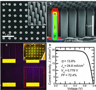
From the industrial point of view, silicon is the most commonly used material. The maximum efficiency for a silicon single junction cells, is about 27.6% for crystalline Si cell84, and about 46% for a multi junction cell84; but increasing the efficiency remains a key issue. The record efficiency, that is demonstrated for thin film solar cells, is about 27.6 % for Si while it is 24.2 %85 for InP, 29.3 %84for GaAs and 22.9 %84for CdTe. Up to the date, the highest recorded efficiency is to the date is 46.0 % from multijunction heterostrucuture84, 85. When compared to the solar light spectrum (with an energy maximum around 1.5eV), InP -1.27 eV,86, 87GaAs-1.43 eV87and CdTe-1.44 eV88 have higher conversion efficiencies than Si –1.11 eV. This explains why the growth of InP and GaAs nanowires is of prime importance for the development of nanowire based solar cells, and is studied on different substrates such as Si89, glass90, glass with Transparent Conductive Oxide (TCO) coating91etc. The record efficiency for a nanowire solar cell is 13.8 % (figure 1.9) using InP nanowires with p-i-n junctions92. In the case of GaAs, and due to the high recombination rate on lateral facets, core-shell GaAs/AlGaAs heterostructures are used in order to passivate surfaces and
Figure 1.9 – Nanowire based solar cell. Characterization of NW-array solar cells: (A) Top-view Scanning Electron Microscopy (SEM) image of a nanowire array (B) Side-Top-view SEM image of the NW solar cell. (C) Optical microscope image of nanowire solar cells. (D) I-V curve (Wallentin et al.92)
1.7
Water Splitting and H
2Generation
H2generation, also known as artificial photosynthesis, is another aspect of the photovoltaic process.
It allows to convert the solar energy into hydrogen (H2) thanks to a Photo Electric Cells (PEC)
using the process of water splitting94, 95. In order to be commercially interesting, an efficiency of at least 5% is necessary. The charge generation process is same than described in the solar cell section (1.6), but the charge collection occurs at the semiconductor/electrolyte hetero-junction interface. The minority carriers react at the surface, while majority carriers travel through the bulk in order to perform complementary reactions at the counter electrode. Hydrogen is produced at the cathode and Oxygen at the anode. The nanowire advantages for this application are: (i) an enhanced light trapping and charge collections, (ii) an enhancement of the redox reaction rate, (iii) and it facilitates the architectural “Z-scheme”96, 97, a concept using two light absorbers, which allows the larger absorption of the solar spectrum and thus larger voltages.
The electrochemical potential of water is 1V, which determines the choice of materials. The series of different chemical reactions that occurs during this process is listed below98:
H2O−→ H2+1 2O2 ∆E = 1.23V CO2+ H2O−→ HCOOH + 1 2O2 ∆E = 1.4V CO2+ H2O−→ HCHO + O2 ∆E = 1.34V 15
1.7. WATER SPLITTING AND H2GENERATION
CO2+ 2H2O−→ CH3OH+
3
2O2 ∆E = 1.21V CO2+ 2H2O−→ CH4+ 2O2 ∆E = 1.06V
Different materials have been studied, including semiconducting nanowires, for both the photo-anode and the photo-cathode. The most promising candidates for photo-cathode are Si99, 100 and InP101 nanowires since they should yield to high current density and high photovoltages. On the other hand, the oxide and III-V based nanowires, including TiO299, n-Fe2O3102, ZnO103, GaN104, 105,
GaP106, InGaP107, InGaN107, and GaAs108 have been used for the photo-anode. The biggest issues, that need to be overcome, are the protection of the electrode surface and the increasing of the redox surface area109.
In order to address these issues, significant research efforts have been devoted to the surface engi-neering. For Instance, heterostructures such as WO3/Fe203110, Fe203/In2O3111and Fe203/MgFe2O4112
increase the absorption range, promote charge transfer, and improve the interface electric field. It is also possible to protect surfaces with a coating layer in order to improve the stability: for example a TiO2 layer over Cu2O nanowires113. Similarly, it is possible to improve the electrode stability
by decorating Cu2O nanowires with Pt nanoparticles114, or depositing CoBi115and CoPi116on BiVo4
nanowires. Recently, the nanotree geometry became extremely popular since it increases the surface to volume ratio. Finally, Liu et al98developed a fully integrated nanosystem (figure 1.10), using a nanotrees geometry with Si as trunk (photo-cathode) and TiO2as branches (photo-anode).
Figure 1.10 – Nanowire based water splitting device. (a) 3D schematic of a nanotree based system and (b) the corresponding band diagram. (Liu et al.98)
1.8
Li-Ion Battery
Sony introduced Li-ion battery for the first time back in 1991 and its demand swore up with the boom of the consumer electronics devices especially mobile phones and laptops. This technology, whose key features are: low cost, longer life span, high current density and good reversibility, remains one of the most active research domain as continuous efforts on improving the technology are crucial for new applications such as hybrid and electric cars. The US Department of energy points out three key requirements in order to establish a consumer market for electrical vehicle using this technology: (i) we should improve the density from 100 WhKg-1 to 150 WhKg-1, (ii) it should withstand at least 1000 charge cycles, and (iii) the price should be decreased by two third117.
As shown in figure 1.11, a Li-ion battery is composed of three major components: the anode, the cathode and an the electrolyte in between. When charging the battery, a Li+ ion from the cathode (mostly LiCoO) passes through the porous and conducting electrolyte towards the anode (mostly graphite). Once it reaches the anode, an intercalcination reaction takes place. The opposite phenomenon is observed during discharge. In this context, the nanowire geometry is attractive for creating low cost and high density electrodes: (i) it allows direct pathways for ions, (ii) the high surface area reduces the charge and discharge time, (iii) the mechanical stability accommodates the volume expansion allowing thus a better lifespan, and (iv) complex architectures are possible with nanowires. Figure 1.11 shows a Li ion battery made of three nanowire modules, which further illustrates these advantages118.
Figure 1.11 – Nanowire based Li-ion battery. (Arvindan et al.118)
A large set of materials has been investigated for both the anode and the cathode. For the anode, the list includes nanowires made of Si119–121, Ge122, SnO
2123, ZnO124, CuO125, Co3O4126, MnO2127,
Fe3O4128etc. Similarly, the oxide based intercalcination materials for the cathode are LiCoO2129,
LiFePO4130and LiMn2O4131nanowires. The high crystalline quality of these oxide based nanowires
enhances the charge and discharge rates with small changes in volume. The mostly used material for the anode is Si, thanks to the high capacity of the Si/SiO2 interface (10 times of the graphite),
but the very high expansion coefficient (300%) of Si nanowires during lithiation makes them fragile 17
1.9. THERMOELECTRICS and reduces the total number of possible cycles132. As a result, a large number of studies have been focused on either reducing the volume expansion of these nanowires by coating them133, 134 or on developing new structures such as porous one135, nanofibres136and heterostructures137, 138.
1.9
Thermoelectrics
The thermoelectric effect is the direct conversion of temperature differences to electric voltage and vice versa via a thermocouple. “A thermoelectric device creates voltage when there is a different temperature on each side. Conversely, when a voltage is applied to it, it creates a temperature difference”139. The term "thermoelectric effect" encompasses two separately identified effects: the Seebeck and the Peltier effect. The Seebeck effect describes the electrical voltage generated from the temperature gradient and thermoelectric generators are based on this principle. The Peltier effect describes the heating or cooling at an electrified junction of two different conductors and thus is implemented in the thermoelectric coolers. The advantage of nanowires is that they provide a perfect platform for improving the themoelectric figure of merit (ZT) by limiting the phonon diffusion along the wires while keeping a good electrical conductivity. At present, the standard value of ZT is 1140, which, if increased to 3, should multiply by 10 the number of possible applications140. Figure 1.12 presents the schematic of a nanowire based thermoelectric generator, where fully vertical Si nanowire arrays are placed between hot and cold electrodes.141
Figure 1.12 – Nanowire based thermoelectric generator. P and N types Si nanowires arrays are placed between hot and cold surfaces via metallic contacts. (Li et al.141)
Mathematically, the Seebeck effect can be described as: S= −∆V
∆ T (1.1)
where S is the Seebeck coefficient, ∆V is the difference in the heat potential and ∆T is the temperature difference. Similarly, the magnitude of the Peltier effect can be represented as :
where Q is the amount of heat that is absorbed or emitted when the current (I) is applied. The relation between S and Π can be expressed as:
Π = T S (1.3) Finally, the most important parameter is the thermoelectric figure of merit (ZT) :
ZT= S
2
σ
k T (1.4)
where S is the Seebeck coefficient, T is the temperature, σ is the electrical conductivity and k is the thermal conductivity. Note that the numerator S2σ is also known as power factor (pf). The equation 1.4 suggests that in order to increase ZT, the material should either have a higher electrical conductivity or a lower thermal conductivity142. The thermal conductivity can be further expressed as143:
k= kelectron+ kphonon (1.5)
where kelectronis the contribution from electrons and kphononis the contribution from phonons.
If we now consider equation 1.4 taking equation 1.5 as a reference, neither conductors nor insulators are better for thermoelectric applications. This can be further simplified:
• Case 1: Increase S : but this will reduce electrical conductivity (insulators)
• Case 2: Increase σ : since electrons are also the heat carriers, the thermal conductivity will also increase (metals)
• Case 3: Increase electrical conductivity (σ ) without increasing the thermal conductivity (k) (semiconductors)
As a consequence, nanoscale semiconductors are the most promising materials for increasing ZT by decreasing kphonon without affecting kelectron. Indeed, in the case of nanowires, it is possible
to decrease the phonon diffusion along the wire by decreasing its diameter without affecting the electrical conduction and thus, to overcome the bulk limitations. In addition, engineering hetero-interfaces along the wire by implementing Quantum Dots (QDs) or Quantum Wells (QWs) can improve the Seebeck coefficient by increasing phonon-surface scattering. The general idea is to create interfaces that electrons will not notice, and where phonons will scatter144.
From the material point of view, Si nanowires145, 146were intensively studied, and even a CMOS compatible nanoscale generator was reported141. The Si1-xGex alloy147 is also advantageous since
it allows to engineer the bandgap, and create axial heterojunctions. However, materials that are historically known for having a high ZT are Bi based chalcogenides such as BiSb148, 149, BiTe150, BiSbTe151, Sb2Se3152etc. The ZT at nanoscale remains a bottleneck since the highest individual ZT
reported for p-type Bi0.5Sb1.5Te3151nanowires is 1.14 at 330K and is 1.59 for β-Zn4Sb3153nanowires
at 675K. Considering bulk materials, the highest reported ZT value is 2.4 by Venkatasubramanian et al.154 in a Bi2Te3/Sb2Te3superlattice thin film device.
1.10. SENSORS
1.10
Sensors
A sensor is a device that produces a measurable signal in response to the external stimulus. The key parameters of a sensor are: accuracy, resolution, signal-to-noise ratio (SNR), drift, sensitivity, selectivity, stability, recovery over time and range. In this context, using semiconducting nanowires can be advantageous since: (i) the large surface area of nanowire based detectors improves some key parameters like sensitivity and response time, (ii) size, weight and power consumption are improved with nanowire sensors, (iii) the SNR is improved since a lot of wires can be used in parallel155and (iv) multiplexing is possible with the help of nanowire arrays156, 157.
Figure 1.13 presents a schematic of a nanowire based sensor. The sensor uses a large number ZnO nanowires to detect H2: when the sensor feels the ambient atmosphere, O2 molecules are
ad-sorbed at the surface, which yields to the creation of O2- and O- species. This causes a surface
depletion of the n-type nanowires, and thus their resistance increases. If the sensor is exposed to a reducing environment such as H2, electrons are released from surfaces and transferred to the
con-duction band. This increases the nanowire conductivity. Similarly, if the environment is composed of oxidizing species such as NO2, the resistance further increases.
Figure 1.13 – 3D schematic of a nanowire based chemical sensor. (a) conventional FET con-figuration and (b) the schottky gated concon-figuration . (Hu et al.158)
The conductivity of the sensor can be expressed as155: G=Πr
2
l neeµe (1.6) Where G is the conductivity of the nanowire under ambient condition, r and l are the radius and the length of the nanowire respectively, (µe) is the electron mobility and (ne) is the electron density
and can be expressed as:
where n0is the electron density prior to the exposure, Nsrepresents chemisorbed species, and α
is the charge transfer coefficient. The sensitivity is the the ratio of the new conductivity with respect to the original one and can be expressed as:
∆ G G = 1 r 2αNs n0 (1.8)
A direct consequence of this equation 1.8 is that sensitivity is improved when nanowires are thinner.
In order to develop chemical sensors, oxide based nanowires, that are the most stable such as ZnO159–164, In2O3165, 166, SnO2167–169, V2O5170, TiO2171, and TeO2172, have been widely used to
detect chemical species including ethanol, NO2, CO, O2, NH3, H2, etc. Apart from these oxide
based nanowires, Pd173, GaN174and Si175nanowires have also been used for fabricating sensors. It
is also possible to improve the sensor properties such as the response time by using Pd clusters176 for SnO2 nanowires, or to develop In177, Sb164, Au178 and Ag178 doping for SnO2nanowires. In
addition, the sensor robustness can be improved by developing nanowire-based FET structures160, and optimizing the signal processing179, 180.
On the other hand, silicon is the most used material for building biosensors181–185 due to its biocompatibility. It is possible to achieve ultra-sensitive probes186, and to improve the robustness by functionnalizing surfaces or using 3D nanostructures such as nanotrees187, 188.
Tools and Methodologies
In this chapter, fabrication and characterization tools, that have been used during the thesis, are introduced. The bottom-up integration of III-V nanowires on silicon is carried out by MBE. The morphological characterizations are probed by Scanning Electron Microscopy (SEM). Transmission Electron Microscopy (TEM) is used for crystallography and composition measurements. X-ray Diffraction (XRD) measurements give the macroscopic composition. Finally, the image processing and data treatment methodology are presented and discussed in details.
2.1
The Molecular Beam Epitaxy
Molecular Beam Epitaxy (MBE) is a growth method that can be characterized by the following sentences: “Atomic layer by layer deposition, ultra-high vacuum environment, atomic abruptness, high purity and fewer defects”. It is a tool for crystal growth in which atom or molecule beams travel from their source to the substrate in an ultra-high vacuum (UHV) environment. This UHV environment (~ 10-11Torr) ensures that elements travel in collision-free conditions until they reach the substrate, leading to the growth of high quality crystal layers. Furthermore, since the growth rate can be as low as 0.01 monolayer/sec (ML/s), the material can be switched from one to another instantly, leading to ultra-thin interfaces.
In the late 1960s, following the technological breakthroughs in electronics and radiofrequency (RF) devices, the demand for high quality III-V compound semiconductors took a peak. In this context, J. R. Arthur and Alfred Y. Cho from the Bell Telephone Laboratories189invented the MBE: a crystal growth technique involving mass transport processes. Within only a few years, MBE got established as a familiar tool not only for high quality crystal growth but also for in-situ charac-terizations. Some of the MBE achievements include the growth of GaAs / AlxGa1-xAs cascade
lasers190, the synthesis of high quality GaAs and AlGaAs superlattices191 and the quantized elec-tron transport192in these superlattice interfaces. This opened an experimental door toward nanoscale bandgap engineering and study of quantum mechanisms in condensed matter. In addition, advanced in-situ characterization tools such as the reflection high-energy electron diffraction (RHEED), or the mass spectroscopy measurements can be implemented in the MBE chamber. Moreover, it is possible
2.1. THE MOLECULAR BEAM EPITAXY to perform surface treatments in the preparation chamber, making thus MBE an ideal platform for studying growth mechanisms.
Figure 2.1 – Riber MBE-412. (1) The loading/unloading chamber, (2) the cluster, (3) the preparation chamber, (4) the parking, (5) the growth chamber and (6) the vacuum system. (http://www.riber.com/assets/files/documentation/mbe412-imp2.pdf)
The system I used during the thesis for nanowire growth is a MBE-412 from Riber (figure 2.1). It is a multi-chamber system composed of four sections: the loading, the cluster, the preparation and the growth one. The loading, preparation and growth chambers are all connected to the cluster. They are hermetically separated by three electro-valves that grant independent UHV and avoid cross contaminations. This system can be operated in a fully automatic mode thanks to Crystal XE: a software developed and distributed by the manufacturer RIBER. Thanks to “batch recipes”, one can program and operate different operations at the same time. This system supports the loading of wafers up to 4 inches. The main features for each chamber is presented in the following sections.
2.1.1 The cluster Manipulator Unused Connectors Pump Parking Robot
Figure 2.2 – 3D schematic of the cluster. [See real picture in Appendix B figure B.1(b)]
The cluster is the central part of the sys-tem since it allows to transfer wafers be-tween the different chambers thanks to an automated central manipulator (figure 2.2) . For this reason, the vacuum level of this chamber is extremely important and is al-ways below 10-9 Torr. In addition, the MBE-412 cluster is equipped with a park-ing zone, allowpark-ing the storage of 5 moly-blocks at the same time under UHV con-ditions. When adding the 10 wafers from the loading, the system can run up to 15
2.1.2 The loading chamber
Manipulator
Loading Door Sample Holder
Pump
Figure 2.3 – 3D schematic of the loading chamber. [See real picture in Appendix B fig-ure B.1(a)]
After ex-situ chemical preparation (if necessary), sam-ples are loaded inside the MBE system via the loading chamber. The figure 2.3 shows a sketch of this cham-ber. Up to 10 wafers can be loaded at the same time in the system. An elevator equipped with a laser barrier al-lows the automatic detection of each moly-block loaded in the system. The UHV environment is achieved thanks to a turbo molecular pump (Varian Turbo-V 551 Naviga-tor), combined with a membrane one. Once wafers are loaded, a pressure of 5x10⁻⁷Torr can be reached within 15 minutes.
2.1.3 The preparation chamber
Figure 2.4 presents a 3D sketch of the preparation cham-ber. The purpose of this chamber is to degas the loaded wafers at an elevated temperature, so that the surface contamination is highly minimized before introduction into the growth chamber. The heating is provided by a series of coil resistances behind the substrate, and a temperature of 750°C can be reached. The UHV envi-ronment is obtained independently in this chamber us-ing the equivalent pumpus-ing configuration than described for the loading.
Oven Sample Holder
Pump
H2 bottle Plasma Cell
Figure 2.4 – 3D schematic of the prepara-tion chamber. [See real picture in Appendix B figure B.1(c)]
In addition to this standard configuration, an in-situ H2 gas / plasma radio-frequency (RF) source is
inte-grated in this chamber (see figure 2.4) for surface prepa-ration. In our setup, the high quality hydrogen is sup-plied thanks to a H2 bottle having a pressure of 40 bar.
The pressure is then regulated thanks to both: a pres-sure regulator and a Mass Air Flow (MAF) controller. The RF cavity, positioned between the MAF controller and and the preparation chamber allows separation of H2into atomic atoms. This plasma cell is turned off if
the desired treatment is H2 gas; whereas the cell is
ig-nited with proper RF power for H2plasma treatment. A
manual valve separates the plasma cell and the prepara-tion chamber, and is only opened during surface treat-ment . More details on H2 treatments can be found in
Appendix A.
2.1. THE MOLECULAR BEAM EPITAXY
2.1.4 The growth chamber
Manipulator Mass Spectometer Effusion Cell RHEED Gun RHEED Screen Flux Gauze Molyblock
Figure 2.5 – 3D schematic of the growth chamber. See real picture in Appendix B fig-ure B.1(d)]
The growth chamber is where the material deposi-tion takes place (figure 2.5). The UHV environment is achieved thanks to a Cryo-Torr 8 Cryopump and an ion pump. A cryopanel placed inside the reactor, and filled with liquid N2, allows to improve further
the vacuum level and thus reduces the contamination level of deposited materials. A sample holder con-trolled by an automated manipulator is located at the center of the chamber. This manipulator rotates at a controlled speed (typically 13 rotations per minute) so that inhomogeneities in the deposition process are avoided. Three spectroscopy tools are present: a flux gauze (above sample holder), a mass spectrometer (at the bottom of the reactor) and RHEED system (gun and display panel are facing each other). The flux gauze is used before each growth in order to cal-ibrate fluxes. The RHEED system allows to measure the growth rate and probe the crystalline structure of the nanowires. The degassed wafers are facing the cells downwards during growth. The temperature is monitored by a thermocouple positioned at the center of the circular heating coils and about 1 cm far from the wafer surface.
The element III sources are standard Knudsen cells (k-cells) and are placed at the bottom hemi-sphere of the reactor facing upwards. The angle between each source and the sample holder is 45°. Note that a k-cell (figure 2.6) consists in an effusion evaporator source, whose flux is controlled by temperature. The III elements are loaded inside a crucible and two thermocouples measure the base and tip temperatures for each cell (figure 2.6). In both cases, a Proportional–Integral–Derivative (PID) controller allows to perfectly stabilize and control the temperature in each zone.
Figure 5: K-cells;(a) Cracker Cell and (b) Effusion Cell
Figure 2.6 – Image of standard Knudsen cells. (www.riber.fr) 26
On the other hand, cracker cells are mostly used for evaporating group V elements (i.e.: As and Sb). The reason is because group V elements are generally evaporated in tetramer forms, whereas dimers are preferred for crystal growth. Indeed, lower defect levels and better material quality are achieved using dimer sources189, which explains the necessity of the cracker zone to transform tertramers into two dimers. Moreover, the cracker cells are equipped with a digital electro-valve allowing full control of the valve opening, and thus a full control of the group V flux (up to 0.01%). Finally, fast changes of the element V flux are possible compared to standard effusion cells limited by the thermal inertia of the source.
The growth chamber is also equipped with a RHEED system (kSA 400), which allows in-situ flux calibrations and structural characterizations. In a RHEED, a collimated mono-energetic electron beam from the RHEED source is directed towards the substrate surface at a grazing angle of about 1° with an energy that lies between 5 − 40 keV. As a consequence, the penetration depth of this beam is limited to the first few atomic layers and, since the energy component perpendicular to the substrate is in the order of 100 eV, creation of defaults is avoided. A CCD camera collects the reflected beam at the opposite side of the electron gun and record the diffraction pattern. The intensity of this pattern oscillates as a function of the surface roughness (figure 2.7). A fully flat surface shows an intensity maximum, while the minimum is observed when half of the next monolayer is grown (see figure 1.6). From the oscillation frequency, it is thus possible to determine the growth rate, which gives an absolute reference for flux calibrations of each III and V element. Using the flux gauge of the system, it is then possible to calibrate fluxes before starting any growth session using Beam Equivalent Pressures . f = 0 f = 0.25 f = 0.50 f = 0.75 f = 1
e-beam ref ect ion
monolayer growt h Rheed int en it
Source : Arthur et al
Figure 6:RHEED Calibaration
Figure 2.7 – RHEED Calibrations. (Arthur189)
2.2. THE ELECTRON MICROSCOPY
2.2
The electron microscopy
“An electron microscope is a microscope that uses a beam of accelerated electrons as a source of illumination. As the wavelength of an electron can be up to 100,000 times shorter than that of visible light photons, electron microscopes have a higher resolving power than light microscopes and can reveal the structure of smaller objects.”193 Indeed, the wavelength of visible light is in the range 400−700 nm, which limits possible observations of nanostructures (smaller visible structures ~300 nm).
From a theoretical point of view, the wavelength of a particle (electron in this case) with a mass (m) and an energy (E) can be expressed as :
λ = √h
2mE (2.1)
where h is the Plank’s constant.
In the case of electrons, the considered wavelength can be controlled thanks to the acceleration energy, making them ideal source for nanoscale microscopy. In an electron microscope, the mag-nification power can be 100,000 times higher than in an optical one. Furthermore, since electrons have mass and charge, they can interact with the studied material and give additionnal informations. Indeed, when interacting with the underlying surface, several components can emerge as presented in figure 2.8. Each of these signals carries different information about the sample and, with adapted tools and filtering techniques, it is possible to measure the crystalline structure, the topography, the strain mapping or the composition of the nanoscale materials.
Figure 7:Electron Interactions on Matter
Figure 2.8 – Electron Matter Interactions 28

![Figure 4.5 presents as-grown SEM images of samples having either a low [4.5(a) 200 °C in green box] or a high [4.5(b) 650 °C in red box] degassing temperature during the H 2 plasma](https://thumb-eu.123doks.com/thumbv2/123doknet/2133777.8665/81.892.229.690.502.1018/figure-presents-images-samples-having-degassing-temperature-plasma.webp)