Fabrication of vertically aligned silicon nanowire arrays and
its application in hybrid heterojunction solar cells
by
Debika BANERJEE
MANUSCRIPT-BASED THESIS PRESENTED TO ÉCOLE DE
TECHNOLOGIE SUPÉRIEURE IN PARTIAL FULFILLMENT FORTHE
DEGREE OF DOCTOR OF PHILOSOPHY
Ph.D.
MONTREAL, AUGUST 29, 2018
ÉCOLE DE TECHNOLOGIE SUPÉRIEURE
UNIVERSITÉ DU QUÉBEC
This Creative Commons licence allows readers to download this work and share it with others as long as the author is credited. The content of this work can’t be modified in any way or used commercially.
BOARD OF EXAMINERS (THESIS PH.D.) THIS THESIS HAS BEEN EVALUATED BY THE FOLLOWING BOARD OF EXAMINERS
Mr. Sylvain G. Cloutier, Thesis Supervisor
Department of Electrical Engineering, École de technologie supérieure Mr. Mohammad Jahazi, President of the Board of Examiners
Department of Mechanical Engineering, École de technologie supérieure Mr. Vahé Nerguizian, Member of the jury
Department of Electrical Engineering, École de technologie supérieure Mrs. Claudine Allen, External Independant Member
Department of Physics, Engineering Physics and Optics, Laval University
THIS THESIS WAS PRENSENTED AND DEFENDED
IN THE PRESENCE OF A BOARD OF EXAMINERS AND PUBLIC JUNE 12, 2018
ACKNOWLEDGEMENTS
I am thankful to Professor Sylvain G. Cloutier for his constant support, encouragement, constructive feedbacks and focused guidance over the past five years. I am thankful to him for influencing me into doing silicon photovoltaics and thus opening an entirely new world for me. I am grateful to him for making my graduate life in ETS very enjoyable and rewarding. He has given me enough freedom to design research projects independently and help me to grow as an independent researcher.
I am thankful to my co-supervisor Professor Véronique François for guiding me through the optics with the nanowire system.
I had the good fortune of collaborating with many talented researchers. I would like to thank Felipe, Jaime, Charles and Xiaohang for collaborating on various parts of this thesis. I would like to acknowledge the technical assistance received from Dr Riad Nechache, Mr. Nelson Landry, Mr. Normand Gravel and Mr. Christian Talbot from our ETS laboratories.
I would also like to thank past and future students in our research group for their support and all the invigorating discussions. Thank you Felipe, Jaime, Charles, FX, Xiaohang, Ivy, Ibtihel, Suchismita, Soraya, Arooba, Sumana and Sayani for their friendship and for making me feel at home.
Special thanks to Charles and FX for helping me to write the thesis abstract in French.
Finally, I would like to thank my father (Mr. Dibakar Banerjee) and my mother (Mrs. Reba Banerjee) for their unconditional support, love and sacrifices.
FABRICATION OF VERTICALLY ALIGNED SILICON NANOWIRE ARRAYS AND ITS APPLICATION IN HYBRID HETEROJUNCTION SOLAR CELLS
Debika BANERJEE
RÉSUMÉ
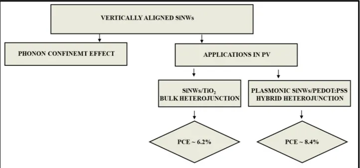
Partout dans le monde, de nombreuses approches pour réduire la sévérité du changement climatique émergent chaque jour. L’énergie photovoltaïque est l'une des avenues attrayantes et efficaces pour la génération d'énergie renouvelable sans carbone. Régnant sur l'industrie photovoltaïque, les cellules solaires à base de silicium cristallin sont efficaces mais coûteuses, en raison de leur complexité de fabrication. Cela amène la motivation à la recherche fondamentale afin de trouver des moyens plus simples et moins coûteux de récolter la lumière et produire de l'électricité. Les plateformes hybrides, à l'aide de la nanotechnologie, s'abordent d'inclure divers matériaux polymères inorganiques et organiques, combinés avec du silicium cristallin, pour fabriquer des cellules solaires hybrides à hétérojonction. L'objectif principal de cette thèse est de développer une méthode rentable pour fabriquer des cellules solaires hybrides à hétérojonction, à base de nanofils de silicium. En raison de leur rapport surface/volume intrinsèquement grand, l'emploi de nanofils de silicium aide à réduire l'utilisation de matériaux et donc le coût de fabrication. Nous avons trouvé la méthode de déplacement galvanique comme étant la technique la plus rentable par rapport aux autres méthodes de synthèse de nanofils de silicium. Les propriétés optiques et électriques de ces nanofils ont été mesurées afin d’évaluer leurs potentiel pour leurs utilisation dans des dispositifs photovoltaïque. Nous avons étudié l'effet de confinement de phonons sur les nanofils de silicium. Le silicium, étant un matériau à bande interdite indirecte; Le confinement de phonons aide à la transition bande à bande des électrons et des trous, ce qui augmente encore l'efficacité photovoltaïque des dispositifs construits autour des nanofils de silicium.
Dans cette thèse, nous introduisons d'abord une architecture de dispositif qui combine des nanofils de silicium et du TiO2 anatase, démontrant la fabrication de cellules solaires à
hétérojonction en utilisant une modification d'interface avec HBr. Cette approche aboutit à des dispositifs PV avec jusqu'à 6,2% d'efficacité de conversion de puissance (PCE) qui représente une amélioration de 3 fois par rapport à des architectures similaires avec une modification d'interface utilisant d'autres voies. Cette thèse offre une voie prometteuse pour l'ingénierie d'interface de dispositifs optoélectroniques hybrides à base d'hétérojonction. La deuxième architecture de dispositif décrite dans cette thèse démontre la fabrication de cellules solaires hybrides à hétérojonction composées de nanofils de silicium et de PEDOT :PSS sensibilisés au plasmon. L'amélioration significative induite grâce aux plasmon est démontrée en contrôlant le processus de nettoyage pendant l'étape de fabrication de nanofils. Ceci permet de laisser une quantité infime de nanoparticules d'argent attachées aux nanofils de silicium avant de les enrober de PEDOT: PSS traité au solvant. Les dispositifs
cellules solaires produites démontrent un PCE allant jusqu'à 8,4% sous AM 1,5G comparer à 5,5% pour les dispositifs sans nanoparticules d'argent. Cette thèse offre un moyen favorable de réaliser des cellules solaires à base de silicium.
FABRICATION OF VERTICALLY ALIGNED SILICON NANOWIRE ARRAYS AND ITS APPLICATION IN HYBRID HETEROJUNCTION SOLAR CELLS
Debika BANERJEE
ABSTRACT
Worldwide, numerous approaches to reduce climate change emerge every day. Photovoltaic is one of the attractive and efficient methods to generate carbon free renewable power. Reigning over the photovoltaics industry, crystalline silicon-based solar cells are efficient but expensive due to their complexity in processing. This brings the motivation for fundamental research in a quest to find of simpler and less expensive ways to harvest light in order to generate electricity. Hybrid platforms, with the help of nanotechnology, strive to include various inorganic, organic, polymer materials combined with crystalline silicon to fabricate hybrid heterojunction solar cells. The main objective of this thesis is to develop a cost-effective method to fabricate silicon nanowire-based hybrid heterojunction solar cells. Employing silicon nanowires help to reduce the material usage and thus the cost by their inherently large surface to volume ratio. We found galvanic displacement method as the most cost-effective technique compared to other methods used for the synthesis of silicon nanowires. Optical and electrical properties of these nanowires have been measured to evaluate the potential of these materials for their usage in photovoltaics. We have investigated phonon confinement effect on the silicon nanowires. Being silicon an indirect band gap material; phonon confinement helps in band to band transition of electrons and holes which further increases the photovoltaic efficiency of devices built around silicon nanowires.
In this thesis, we first introduce a device architecture that combines silicon nanowires and anatase TiO2, demonstrating the fabrication of bulk heterojunction solar cells using interface
modification with HBr. This approach results in PV devices with up to 6.2% of power conversion efficiency (PCE) that represents 3 times enhancement compared to similar architectures with interface modification using other routes. This thesis provides a promising route for interface engineering of hybrid heterojunction based optoelectronic devices.
The second device architecture described in this thesis shows the fabrication of hybrid heterojunction solar cells comprised of plasmon sensitized silicon nanowires and PEDOT:PSS. Significant plasmon induced enhancement is demonstrated by controlling the cleaning protocol during the nanowire fabrication step. This allows to leave minute amount of silver nanoparticles attached to the silicon nanowires before coating with solvent treated PEDOT:PSS. The solar cell devices produced show a PCE up to 8.4% under AM 1.5G compared to 5.5% without silver nanoparticles. This thesis yields a favorable way to achieve better performing ultra-low-cost silicon-based solar cells.
TABLE OF CONTENTS
INTRODUCTION... CHAPTER 1 STATE OF THE ART………... 1.1 The importance of solar enery……….. 1.2 Materials used for fabricating solar cells……….. 1.3 Sources of losses in solar cells……….. 1.4 Efficiency enhancement techniques of solar cells using vertically aligned SiNWs….. 1.5 Efficiency enhancement techniques using modelling/simulations………... 1.6 Efficiency enhancement techniques using phonon confinement mechanism………... 1.7 Efficiency enhancement techniques by interface modifications………... 1.8 Efficiency enhancement techniques by incorporating silver plasmons……….. CHAPTER 2 OVERALL RESEARCH OUTLINE………... 2.1 Research outline for low cost solar cells... 2.1.1 Objectives for probing phonon processes in vertically aligned SiNWs………... 2.1.2 Objectives for fabricating SiNWs-based heterojunction solar cells……… 2.2 Outline of the thesis chapters……… CHAPTER 3 LITERATURE REVIEW………... 3.1 Silicon nanowires...…... 3.2 Galvanic displacement method (GDM)………... 3.3 Rigorous coupled wave analysis (RCWA)………. 3.4 Phonon confinement effect in silicon nanowires………..……... 3.5 Silicon nanowires-based heterojunctions for PV applications……… CHAPTER 4 SIMULATION WORKS TO DETERMINE THE OPTICAL
PROPERTIES OF THE SILICON NANOWIRES………. 4.1 Introduction………...
4.2 Design of the modelling………. 4.3 Results……….. 4.4 Conclusions………... CHAPTER 5 PHONON PROCESSES IN VERTICALLY ALIGNED SILICON NANOWIRE ARRAYS PRODUCED BY LOW-COST ALL-
SOLUTION GALVANIC DISPLACEMENT METHOD..………... 5.1 Introduction………...
5.2 Experimental methods………. 5.2.1 Synthesis of the vertically aligned silicon nanowires arrays……….. 5.2.2 Studying the phonon localization effect……….. 5.2.3 Studying the chemical composition contamination at the surface………..
1 3 3 4 4 7 9 9 10 10 11 11 11 11 12 13 13 15 19 20 22 27 27 27 29 30 31 31 33 33 35 35 Page
5.3 Results and discussions……….. 5.4 Conclusions………... CHAPTER 6 TAILORED INTERFACES OF THE BULK SILICON NANOWIRE/TiO2
HETEROJUNCTION PROMOTING ENHANCED PHOTOVOLTAIC PERFORMANCES……… 6.1 Introduction………...………... 6.2 Results and discussions………... 6.2.1 Structure of the solar cells………. 6.2.2 Performance of the solar cells………... 6.2.3 Role of surface treatment using HBr and HF in SiNWs/TiO2 solar cells……….
6.3 Conclusion………... 6.4 Experimental methods………... 6.4.1 Synthesis of vertically aligned silicon nanowires………... 6.4.2 Synthesis of TiO2 sol-gel………..
6.4.3 Formation of the heterojunction……… 6.4.4 Contact fabrication………
6.4.5 Device characterization………... CHAPTER 7 PLASMON ENHANCED SILICON NANOWIRE ARRAY-BASED
HYBRID HETEROJUNCTION SOLAR CELLS………... 7.1 Introduction………... 7.2 Results and discussions………... 7.2.1 Plasmonic response of SiNWs………... 7.2.2 The hybrid organic-inorganic heterojunction solar cells………...……….. 7.2.3 Performance of the solar cells……….. 7.3 Conclusion………. 7.4 Methods………. 7.4.1 Synthesis of plasmon sensitized silicon nanowires………. 7.4.2 Formation of the hybrid heterojunction………... 7.4.3 Contact structure………..
7.4.4 Materials and device characterization……….. CHAPTER 8 CONCLUSIONS………...
CHAPTER 9 STATEMENT OF ORIGINAL CONTRIBUTIONS AND FUTURE WORKS………. 9.1 Statement of original contributions………... 9.2 Future works………… ………... 9.2.1 Room temperature fabrication of silicon hybrid photovoltaics using
amorphous TiO2………...
9.2.2 Fabrication of plasmon sensitized SiNWs/TiO2 heterojunction for
Photovoltaic application………... 9.2.3 Characterization of plasmonic response in nanowire solar cells by
controling the plasmons size distributions………... 54 54 55 55 63 63 65 65 66 67 71 71 71 72 72 73 81 83 83 83 83 84 84 48 48 51 53 53 53 49 35 38 45 45
LIST OF PUBLICATIONS………. LIST OF REFERENCES………. ANNEX I………. ANNEX II……… 85 87 107 111
LIST OF TABLES
Table 4.1 Calculated solar cells efficiencies……….………... Table AIS1 EDX analysis of the atomic percentage of oxygen present in the nanowire Samples treated with different concentrations of acids……….. Table AIS2 EDX analysis of the atomic percentage of oxygen present in the nanowire Samples for different treatment time……….. Table AIS3 Photovoltaic characteristics of group 1 solar cells………. Table AIS4 Photovoltaic characteristics of group 2 solar cells………. Table AIS5 Photovoltaic characteristics of group 3 solar cells……..……… Table AIIS1 Identification and quantification of elements from the XPS survey scan... Table AIIS2 Photovoltaic characteristics of all solar cells from group 1…………..……. Table AIIS3 Photovoltaic characteristics of all solar cells from group 2……… Table AIIS4 Photovoltaic characteristics of all solar cells from group 3…..……….
30 108 108 109 109 110 114 114 115 115 Page
LIST OF FIGURES
Figure 1.1 Thickness dependence of (upper image) Filling Factor (FF) and (lower image) efficiency for (1:1) P3HT:PCBM (squares) and (1:4) OC1C10PPV: PCBM
(triangles) PV ……….………. Figure 1.2 Heterojunction morphology aimed to improve carrier collection. The image shows a multilayer heterojunction that requires multiple deposition steps and post growth processing to contact individual layers……… Figure 2.1 Schematic outline of the overall thesis research………... Figure 3.1 Left column indicates the lateral view of the typical one step etching process and right column indicates the top view of the same etching process……... Figure 3.2 (a) E-k diagram for direct bandgap material, (b) E-k diagram for indirect Bandgap materia……….. Figure 3.3 Traditional single junction solar cell (left). 3D nanowire solar cell (right)……. Figure 3.4 Radial pn junction Si wire array solar cell geometry, Inset: SEM image of polymer embodied SiNW array……….. Figure 4.1 Upper image: Model geometry uses for SHA 2D tool (region in red color is air, green colored region is silicon nanowire and blue region is the silicon substrate). Lower image: Optical properties vs. wavelength plot in 3nm spacing (length of the nanowire 400 nm and diameter 100 nm)……….. Figure 4.2 Optical properties vs. wavelength plot in 3 nm spacing (length of the nanowire 1 µm and diameter 100 nm)……….
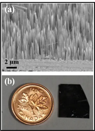
Figure 5.1 (a) SEM micrograph of the silicon nanowire arrays synthesized using GDM, (b) Top-view of the nanostructured silicon sample, highlighting the uniformity and the strong anti-reflection behaviour of the nanoengineered surface……….. Figure 5.2 (a) Cross-sectional view of the cleaved nanostructured-silicon wafer. (b) Silicon Raman peak intensity distribution using 532 nm excitation laser. The top of the nanostructured area (tips of the nanowires) shows much stronger Raman signal. (c) Silicon Raman peak’s width distribution showing larger FWHM at the top of the nanostructured region. (d) Silicon Raman peak’s position showing a significantly down-shifted Raman peak at the top of the nanostructured region………... 5 7 12 17 21 24 25 29 30 40 41 Page
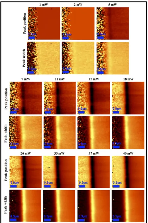
Figure 5.3 Spatial distribution of the nanostructured silicon’s Raman peak and width with increasing laser power (left region is air, middle region is the top parts of the nanowires) All the scale bars are 0.9 µm………. Figure 5.4 (a) Evolution of silicon Raman peak position and (b) Evolution of silicon Raman peak width with increasing laser power. The blue diamonds (♦) Represent the silicon substrate and red dots (●) represent the silicon
nanowires………. Figure 5.5 Nanostructured silicon’s Raman peak shift-width evolution with increasing laser power. The blue diamonds (♦) represent the silicon substrate and red dots (●) represent the silicon nanowires……….. Figure 6.1 (a) Band diagram of n-n isotype heterojunction (left), band diagram of p-n heterojunction (right), (b) Schematic of n SiNWs/TiO2 heterojunction solar
cell……… Figure 6.2 (a) SEM micrograph of the silicon nanowire array structure synthesized using GDM, (b) Raman peaks for anatase TiO2 on SiNWs, (c) and (d) SEM
micrographs of the SiNWs/TiO2 bulk heterojunction………..
Figure 6.3 (a) J-V curve of the heterojunction solar cells under AM 1.5G from group 1 devices, (b) J-V curve from group 2 devices, (c) J-V curve from group 3 devices, (d), J-V curve of best performing devices from each group………….. Figure 6.4 (a) Log-plot of the dark current of group 1 devices, (b) Log-plot of the dark current of group 2 devices, (c) log-plot of the dark current of group 3 devices, (d), Log-plot of the dark current of best performing devices from each group.. ………. Figure 6.5 Histogram plots of the solar cell parameters: (a) Power conversion efficiency (ƞ), (b) Short circuit current density (Jsc), (c) Open circuit voltage (Voc), (d) Fill
factor (FF) of the 24 devices from 3 different groups……….. Figure 6.6 XPS spectra of (a) Si 2p, (b) O 1s, (c) C 1s peaks from the pristine (non- treated) (black), HF treated (red) and HBr treated (green) SiNWs samples…… Figure 7.1 (a) Si nanowires covered with Ag dendrites after GDM. (b) Ag nanoparticle- decorated Si nanowires after removal of the Ag dendrites only. (c) Si
nanowires after complete removal of the Ag………... Figure 7.2 (a) XPS spectra of Si nanowires with Ag dendrites, (b) XPS spectra of Si nanowires decorated with Ag nanoparticles, (c) Ag survey of Si nanowires with Ag dendrites, (d) Ag survey of Si nanowires decorated with Ag
nanoparticles……… 58 59 60 61 74 75 44 56 57 42 43
Figure 7.3 Optical reflectance (% R) of Si nanowires arrays with and without minute amounts of Ag nanoparticles………... Figure 7.4 (a) Schematic of the hybrid heterojunction solar cells, (b) energy band diagram of the hybrid heterostructure………... Figure 7.5 J-V characteristics of the solar cells under illumination. (a) Si/PEDOT:PSS (device 1-4 treated with IPA and device 5-8 treated with SDS), (b)
SiNWs/PEDOT:PSS (device 1-4 treated with IPA and device 5-8 treated with SDS), (c) plasmonic SiNWs/PEDOT:PSS (device 1-4 treated with IPA and Device 5-8 treated with SDS), (d) best devices from a,b and c……… Figure 7.6 Histogram plots of the solar cell parameters of the 24 devices from 3 different groups: (a) Power conversion efficiency (PCE), (b) Short circuit current density (Jsc), (c) Open circuit voltage (Voc), (d) Fill factor (FF)……….
Figure 7.7 (a) EQE and (b) IQE of the samples from each groups……… Figure AIS1 SEM micrographs of (a) silicon nanowire array structure synthesized using GDM, (b) SiNWs/TiO2 bulk heterojunction………...
Figure AIIS1 SEM images of (a) SiNWs/PEDOT:PSS heterojunction at 40o tilted condition
(b) Top view of SiNWs/PEDOT:PSS heterojunction at 40o tilted condition….
Figure AIIS2 (a) Schematic of solvent-treated PEDOT:PSS droplet on plasmonic nanowire surface for measuring the contact angle, (b) SDS-treated PEDOT:PSS droplet on pristine Si, (c) SDS-treated PEDOT:PSS droplet on SiNWs and (d) SDS- treated PEDOT:PSS droplet on plasmonic SiNWs samples……….. Figure AIIS3 IPA-treated PEDOT:PSS droplet on (a) Pristine Si, (b) SiNWs and (c)
Plasmonic SiNWs samples……….. Figure AIIS4 Schematic of the pristine and SDS-treated PEDOT:PSS………
78 79 80 107 111 112 112 113 76 77
LIST OF ABREVIATIONS
GDM Galvanic displacement method
MAWCE Metal assisted wet chemical etching NPs Nanoparticles NWs Nanowires
PCE Power conversion efficiency
RCWA Rigorous coupled wave analysis
SPR Surface plasmon resonance
LIST OF SYMBOLS
Ag Silver H Hydrogen
HBr Hydro bromic acid
HNO3 Nitric acid
FF Fill factor
Isc Short-circuit current
Jsc Short-circuit current density
N2 Nitrogen
O2 Oxygen
Si Silicon
INTRODUCTION
I have selected the option of writing the experimental part in original paper-based research works according to the ETS thesis preparation and submission policies. These manuscripts consist of chapter 5-7 of this thesis. Each chapter comprises of an abstract, introduction, results and discussions and experimental methods. Additionally, this thesis consists of an overall abstract, introduction, research outline, literature review, conclusions, and statement of original contributions and future works.
Chapter 1 explains the fundamental technologies of solar cells including different techniques to increase the efficiency of SiNWs-based hybrid solar cells.
Chapter 2 describes the overall research outline of this thesis.
Chapter 3 comprises of an extensive literature review for this thesis work.
Chapter 4 consists of the simulation works to determine the optical properties of the silicon nanowires.
The chapters 5-7 demonstrate the studies performed to accomplish the research goals. Chapter 5 investigates the phonon confinement effect on vertically aligned SiNWs. Phonon confinement effect can increase the band-to-band transitions in Si to potentially increase the conversion efficiencies in SiNWs based photovoltaic devices. Unfortunately, producing nanowires exploiting nanoscale confinement to achieve the phonon localization effect can be a costly process. Here we report on the observation of such phonon-localization effect in SiNWs fabricated at very low-cost without chemically altering Si using an all-solution based metal assisted wet chemical etching (MAWCE) method.
Chapter 6 illustrates the photovoltaic performance of HBr treated SiNWs/TiO2 n+-n bulk
dye-sensitized solar cells as well as a transparent front contact in heterojunction solar cells. Unfortunately, few reports are available where TiO2 is used as the main component for single
heterojunction fabrication with Si. It is because previously works are focused on fabricating devices using narrow bandgap semiconductors. Here we report a feasible route for low cost, all solution based, easily available n-SiNW/n-TiO2 isotype heterojunction for photovoltaic
device by interface-modification using HBr.
Chapter 7 demonstrates about significant plasmon-induced enhancement to achieve better ultra-low-cost solar cell devices. Recently, hybrid silicon nanowire based heterojunction solar cells attracted attention in the photovoltaic market due to their high photovoltaic potential and low processing costs. Here we report how strong localized surface plasmon modes induced using silver (Ag) nanoparticles can be used to achieve significant improvement in a simple hybrid organic inorganic photovoltaic device between n-type silicon nanowires (SiNWs) and poly(3,4-ethylenedioxythiophene):poly-(styrenesulfonate) (PEDOT:PSS).
In this research duration, I was able to contribute to 8 peer-reviewed journal articles (published/in press/submitted/to be submitted) with 5 as first author and 3 as a co-author. From this, I have picked up 3 articles pertaining to the thesis research goal, in which I am the first author.
STATE OF THE ART
1.1 The Importance of Solar Energy:
Solar energy is important for humans, animals and plants. Humans and animals use sunlight for synthesis of vitamin D (Dincer, 2000). Solar energy is used as a source of clean energy since it does not harm the ecosystem. Most importantly, solar energy is versatile. It can be used to produce power for many appliances (cooking, cars, watches, calculators etc.) as well as it can produce electricity to run the entire world. It is a source of renewable energy which will become the only source of energy in the future since fossils fuels will come to an end (Höök et Tang, 2013). This is because, we have consumed an improbable amount of fossil fuels since the ancient times. The rate of consuming the fossil fuels is increasing with world’s population. Hence it will run out faster in near future. Fossil fuels also affect the atmosphere. It is responsible for global warming and climate change due to growing levels of certain toxic gases in the environment. Therefore it is necessary to switch to green energy to avoid these fossil-fueled problems.
The energy in light is converted into electrical power in a solar cell (Heeger, 2014). Sunlight contains photons that hit the solar panel and get absorbed by the semiconducting materials of the panel. It helps to knock the electrons to loose from their atoms and flow as electric current (Kim et al., 2013).
1.2 Materials Used for Fabricating Solar Cells:
Solar cells can be made from various materials- inorganic or organic (Noh et al., 2013). Direct band gap materials such as GaAs, InP, CdTe give more energy conversion efficiency than indirect ones e.g. Ge, Si (Shah et al., 1999). Metals like Ag, Al, Au, Cu, Zn can be used to fabricate solar cells and insulators like glass is also a very good substrate to design a solar cell (Kluth et al., 1999). For this thesis research, we will fabricate solar cells using silicon (Si) wafer since in the crystalline form, Si has lot of special chemical properties (Wenham et Green, 1996). Moreover, Si is not toxic and is found in nature in abundance.
1.3 Sources of Losses in Solar Cells:
There are four important loss mechanisms (Kaushika et Rai, 2007) that need to be analyzed in solar cells namely a) photon absorption, b) exciton generation, c) exciton separation into free carriers, and d) carrier collection by electrodes.
Photon absorption is the ability of a solar cell to capture and preserve as many photons reaching its surface. Photons in the sunlight hit the solar cell and are absorbed by the semiconducting solar cell material. However, material surface defects, angle of incidence and difference in index of refraction make this task a tough one to achieve (Trupke, Green et Würfel, 2002a).
There are two main sources of loss in photon absorption: i) reflection, for which certain portion of the incident light manages to enter the active region of the device and the rest is reflected (Zhao et al., 1995), and ii) transmission, which strongly depends on the material and active region thickness (Trupke, Green et Würfel, 2002b). An active region too thin, in the order of 100 nm or less will not take full advantage of the photon collection, and one too thick, on the order of 1 um or more presents difficulties for fabrication with desired precision. Thickness in the active region affect directly operation parameters such as short circuit current density, filling factor and efficiency, as can be seen in figure 1.1 (Moulé, Bonekamp et Meerholz, 2006).
Reflection loss can be significantly reduced by the addition of antireflection coatings and micro grooving the cell surface (Zhao et Green, 1991). These modifications make the surface an appropriate interface for light to go through at different wavelengths at normal incidence. To maximize this wavelength range, several layers of antireflection coating are used in which is each layer is more sensitive to a certain wavelength value. In comparison, a Si solar cell without any antireflection coating loses 30% or more of the incident light to reflection (Zhao et Green, 1991).
Figure 1.1 Thickness dependence of (upper image) Filling Factor (FF) and (lower image) efficiency for (1:1) P3HT:PCBM (squares) and (1:4) OC1C10PPV: PCBM (triangles) PV
Taken from (Moulé, Bonekamp et Meerholz, 2006)
The second loss mechanism is exciton formation inside the cell. A clear confirmation of a photon being absorbed is the creation of an exciton, which is an electron-hole pair bound by Coulomb potential. If this binding energy is smaller than the device's thermal energy at room
temperature, the exciton will break and the carriers will relax to the band edges as free charge carriers that can be further extracted. If the binding energy is strong, a bound exciton state will be formed by the carriers, as is the case for organic semiconductors (Knupfer, 2003), and the carriers will be relaxed due to carrier phonon coupling. As a result, the energy will be dissipated by heat transfer. This loss mechanism accounts for 30-40% of the incident solar radiation (Garnett et al., 2011). Additionally, carrier relaxation losses are related to the charge separation processes that are due to the potential gradient in the active region. In the end, it facilitates the carrier collection by the contact interfaces.
On the other hand, carrier relaxation losses are controlled by using alloys of materials with different bandgaps in order to reduce the heat losses, but materials such as indium gallium nitride show a miscibility gap at intermediate concentrations due to large lattice mismatch strains. Figure 1.2 presents a general schematic of a multilayer solar cell. Another approach to improve this condition is by using high purity single crystalline substrates with a large minority carrier diffusion length that will greatly enhance carrier separation for further collection (Ellingson et al., 2005).
Figure 1.2 Heterojunction morphology aimed to improve carrier collection
The image shows a multilayer heterojunction that requires multiple deposition steps and post growth processing to contact individual layers
Adapted from (Ellingson et al., 2005)
1.4 Efficiency Enhancement Techniques of Solar cells using Vertically Aligned Silicon Nanowires:
A significant amount of research has gone into understanding the unique electrical, mechanical and thermal properties of nanowires (NWs) (Thelander et al., 2006). The Si based NWs have become popular since adequate industrial infrastructure can help to fabricate SiNWs at low manufacturing costs. Typically diameters of nanowires tune on the order of nanometres. The motivation for research on NWs arises from the fact that electrons in nanowires are restricted in the lateral direction occupying energy levels different from the energy levels found in bulk materials. For this reason, SiNWs show luminescence. On the other hand, indirect band gap SiNWs can barely be used in functional optoelectronics. These two qualities together and the formation of SiNWs which are electrically and optically porous can steer new generation of Si based nanoscale devices. The other advantage of using NWs is that these tiny architectures can be assembled without complex and costly fabrication facilities making device fabrication a cheap endeavor. Applications of NWs are investigated in different fields such as field-effect transistors (FETs) (Goldberger et al., 2006), flexible large area electronics, thermoelectric, photovoltaics (Garnett et Yang, 2008), battery electrodes (Peng et al., 2008), and electronic biosensors (Zheng et al., 2005).
While there are various routes available to obtain uniform NW arrays, doping concentration in the substrate material remains to be one of the key issues in the fabrication and performance of NW-based devices (Hochbaum et al., 2008). As it stands, the popular doping methods are thermal diffusion, ion implantation and in-situ doping during growth of the nanowires (Lauhon et al., 2002). However these methods still suffer from the disadvantages of increased crystallographic defects and doping fluctuations at high doping levels. Additionally, most of these methods have the need of either high temperatures processing or prolonged fabrication times attributed to the limitations of the growth mechanisms. Therefore, obtaining accurate doping concentrations in large-area aligned NWs remains to be a challenging problem.
Till date, different methods have been developed to manufacture SiNWs such as chemical vapor deposition using the VLS (Vapor Liquid Solid) technique, laser ablation, thermal evaporation decomposition, molecular beam epitaxy, chemical etching, and solution growth (Holmes et al., 2000; Ryan et Barrett, 2012; Westwater et al., 1997; Zhang et al., 2008). Among these methods, metal assisted wet electroless chemical etching (MAWCE) (Ng et al., 2011; Zhang et al., 2008) of Si substrates is an attractive method for the fabrication of these tiny systems. This is because of the following reasons (a) the fabrication route involved is a low-cost approach (b) the NWs produced using this technique show very small values of reflectance which is why these systems have the potential for usage in photovoltaic applications (c) the resulting NWs have the potential for effective use in self-powered functional nanoelectronic systems. The key feature of this technique is selective electrochemical etching of Si using metal catalysts which results in well organized and highly dense arrays of SiNWs with identical crystallographic orientations. In addition, ordered SiNWs with structural dimensions on the orders of hundreds of nanometres can be fabricated using this technique.
1.5 Efficiency Enhancement Techniques using Modelling/Simulations:
With recent developments in materials processing technology, there is a growing need for optimization of device performance by careful selection of materials, device design. Currently, silicon nanowire based solar cells have been shown to reach an ultimate efficiency of 20 % which is still far from the maximum theoretical efficiency of 34% predicted. This gap between theoretical and experimental efficiencies can be minimized by understanding the loss mechanisms. This objective can be realized in two ways. The first choice is to understand the effect of materials, sizes on the loss mechanisms by performing careful experiments which is a costly endeavour. The other way is to perform simulations to understand these different mechanisms. The advantage of simulation techniques is that they are cost effective and less time consuming. The simulation techniques adopted till date can be categorized in two classes : i) continuum based analytical techniques, e.g analytical slovers for Rigorous coupled wave analysis (RCWA) (Xie, Oh et Shen, 2011) ii) finite element techniques to solve for based on Maxwell’s equation of electromagnetic waves (Gao, Yu et Huang, 2006).
1.6 Efficiency Enhancement Techniques using Phonon Confinement Mechanism:
Phonon confinement effect plays an important role to increase the conversion of energy in solar cells based on SiNWs (Richter, Wang et Ley, 1981). Crystalline Si has an indirect band gap of 1.1 eV which is not good for efficient light emission. Exciton binding energy for crystalline Si is also very small ≈ 15 meV. Phonon confinement mechanism changes the indirect nature of band structure for crystalline Si. This effect can be measured using Raman spectroscopy (Adu et al., 2006). SiNWs with very small diameters (<20nm) can show phonon confinement effect which helps to increase the optical transition of SiNWs based solar cells (Piscanec et al., 2003). In this thesis, we have investigated phonon confinement process in vertically aligned SiNWs.
1.7 Efficiency Enhancement Techniques by interface modifications:
Surface recombination (Tiedje et al., 1984) plays an important role to reduce the performance of solar cells. Researchers used different techniques of surface passivation (Aberle, 2000) to limit the surface recombination. Thin film layer depositions of SiO2, Al2O3 etc. are very
popular techniques to passivate the device surface (Jan, Mark et Andrés, 2001; Schmidt et al., 2008). For, SiNWs based devices, cleaning the native oxide layer from the nanowire surface before the junction formation helps to enhance the photovoltaic performance (McAlpine et al., 2007). HF treatment (Ma et al., 2003) is the most well-known for removing native oxide layer from the nanowire surface. In this thesis we have explored a new route for surface passivation using HBr which boosts the efficiency of SiNWs/TiO2 bulk
heterojunction solar cells by 3 folds compared to the similar devices treated with HF.
1.8 Efficiency enhancement techniques by incorporating silver plasmons:
Silver (Ag) plasmons help to absorb the UV light from the solar spectrum (Wang et al., 2009). In this thesis, we have explained significant plasmon induced efficiency increment in low-cost hybrid solar cells comprised of plasmon sensitized SiNWs and PEDOT:PSS. We observed reduced reflectance in UV/VIS region for plasmonic SiNWs. A significant efficiency enhancement of 52% has been noticed when minute amounts of Ag plasmons are incorporated with SiNWs/PEDOT:PSS solar cells compared to the similar structure without Ag plasmons.
OVERALL RESEARCH OUTLINE
2.1 Research outline for low-cost solar cells :
2.1.1 Objectives for probing phonon processes in vertically aligned SiNWs :
The primary objective of this part of the thesis is to probe the phonon localization process in vertically aligned SiNWs to improve the band to band transition in SiNWs-based optoelectronic devices. The specific objectives of this part are:
• To investigate the phonon confinement effect using high resolution Raman spectroscopy; • To establish a cost-effective route to achieve phonon localization effect in SiNWs since
fabricating nanowires to exploit nanoscale confinement can be a costly method;
• To eliminate the other possibilities like surface enhanced Raman effect, laser-induced heating etc. that can cause the change in contrast of the results from Raman spectroscopy.
2.1.2 Objectives for fabricating SiNWs-based heterojunction solar cells :
The primary objective of this part is to develop new routes to fabricate cheap and efficient SiNWs-based heterojunction solar cells. The specific research objectives are:
• To establish a new path to fabricate SiNWs/TiO2 bulk heterojunction solar cells;
• To develop a new process to passivate the dangling bonds from the SiNWs surface which will help in enhancing the optoelectronic properties of the solar cells;
• To study the plasmonic effect in SiNWs and implement it in fabricating hybrid heterojunction solar cells;
• To process the solution of organic materials (PEDOT:PSS) to increase its conductivity and use it to fabricate hybrid heterojunction solar cells in conjunction with plasmon sensitized SiNWs;
• To increase the overall efficiency of existing solar cells by employing different materials; • To reduce the cost of solar cells by all solution based fabrication process.
2.2 Outline of thesis chapters :
This thesis is divided into 8 chapters. Chapter 1 depicts the background and research objectives of this thesis. Chapter 2 demonstrates the research outline followed by an extensive literature survey in chapter 3. Chapter 4 consists of the simulation works carried out to determine the optical properties of the nanowires. Chapters 5-7 are original research articles published. These articles include the main studies performed to achieve the thesis objectives. Figure 2.1 demonstrates an overall outline of the areas covered to achieve the objectives. Chapter 8 describes the overall conclusion from this thesis. Statement of original contributions from this research and future works are included in chapter 9.
LITERATURE REVIEW
3.1 Silicon Nanowires:
In general silicon nanowire synthesis techniques can be broadly classified into the following categories. :
Bottom-up approach: nanowires nucleation and growth takes place at the substrate surface
from molecular precursors using nanoparticles as catalyst.
Top-down approach: nanowires growth starts at the substrate surface and continues through
the bulk through the patterned areas.
The most popular bottom-up approach for the synthesis of SiNWs is vapor-liquid-solid (VLS) technique (Westwater et al., 1997). It is one of the most attractive techniques used for the growth of silicon nanowires structures using Chemical Vapor Deposition (CVD) (Hofmann et al., 2003). In this method, first silicon forms vapor phase which then passes all the way through a liquid droplet becoming a solid. Usually, the growth of a crystal from a gas against a solid surface by means of adsorption is a sluggish process. In VLS technique this problem is taken care of by using a liquid alloy to rapidly adsorb silicon from a supersaturated vapor. Afterwards crystal growth takes place from these sites at the liquid– solid interface. The physical nature of SiNWs grown using this technique can be controlled by the physical properties of the liquid alloy(Hofmann et al., 2003).
Other than CVD some other methods can be combined with VLS to fabricate SiNWs. These techniques are Molecular beam epitaxy (MBE) (Fuhrmann et al., 2005), Laser ablation (Zhang et al., 1998), Evaporation of silicon (Niu, Sha et Yang, 2004). MBE uses high-purity silicon source which is heated at high temperatures to make it evaporate. MBE is carried out
at ultra-high vacuum levels to reduce contamination and allow monitoring of the growth, surface structure while fabrication. Gaseous beam of evaporated silicon atoms or molecules is directed onto the substrate so that the atoms gets absorbed leading to crystallization.
In addition to VLS the other methods which belong to the bottom-up approach are, (i) Oxide assisted growth technique, (ii) Solution-liquid-solid (SLS) method and (iii) Template-directed synthesis method.
In the oxide-assisted growth (OAG) method (Lee et al., 2013), oxides are used for facilitating the formation of nanowires. The major advantage of this approach is that no metal catalysts are needed in the process. This eliminates the risk of contamination in the material, thus the performance of nanowires are better.
Compared to VLS technique, SLS method employs an organic solvent for the growth of NWs at atmospheric pressure. This technique was first implemented by Korgel et al. by effectively producing SiNWs with diameters of few nanometres and lengths up to few micrometers. They used a supercritical fluid as the solvent (Holmes et al., 2000).
In template-directed method the template acts as a platform to generate the raw material in situ. In addition to it the sample formed into a nanostructure with its morphology matching to that of the template (Q. Peng, P. Huang et Zhu, 2004; Xia et al., 2003). The advantages of this technique can be summarized as e.g., easy fabrication, controllable compositions and distribution, uniform size of nanostructures compared to fabrication methods.
Primary challenges for bottom-up approach based NW fabrication methods are controlling diameter and orientation of the nanowires. These problems affect the efficiency of the fabrication of NW arrays.
On the other hand, top-down approach is much more attractive for batch production of ordered nanowires. Top-down methods have gained popularity for the fabrication of ordered SiNWs arrays in terms of crystallographic orientation, diameter, length and position. These
techniques can be broadly categorized into two classes based on the orientation of the NWs. The first category belongs to horizontal nanowires lying on the substrate plane which is most often associated with lithography and dry or wet etching steps. The second category belongs to vertical nanowires which are oriented in normal to the surface of the substrate. These NWs are fabricated using reactive-ion etching or wet chemical etching.
Metal-assisted wet-chemical etching of silicon substrates for fabricating SiNWs is one of the top-down techniques. It is considered as a potential route for mass production of ordered vertically aligned nanowires because of the following reasons. Using this technique one can have exercise exact control over the geometry of the structure i.e. diameter, length, spacing. The most important fact is that all of these can be achieved avoiding high-cost and low-output usual lithographic processes. This technique is based on the principles of galvanic displacement (Carraro, Maboudian et Magagnin, 2007) reaction, details of which are discussed below:
3.2 Galvanic Displacement Method (GDM):
Galvanic displacement is defined by the process of natural reduction of a metal by another metal above it in the electromotive series (Peng et al., 2002). This technique is frequently used for metal depositions with nanoscale control. To do this, the desired metal ions are dissolved in aqueous solutions and which are then readily reduced to atoms during the oxidation of the substrate material. Generally, metals whose redox potentials are higher than hydrogen are deposited using this method. However, for this technique to be successful the substrate material should be oxidizeable.
In general, metal assisted wet electroless etching is categorized into two classes, which are processes involving one-step and two-step chemical reactions. In this technique SiNWs are fabricated by selective chemical etching of silicon substrates in aqueous acid solutions. Nanoparticles of metals which act as catalysts are deposited on the substrate surface (Peng et al., 2005).
The processes in the one-step reaction involve concurrent reduction of metal ions, and oxidation, dissolution of silicon. The etching mechanism in an aqueous solution of hydrofluoric acid (HF) containing silver nitrate (AgNO3) has been studied in details (Q.
Peng, P. Huang et Zhu, 2004). As is described in Equation 1, the first step in this process is the formation of an Ag+ ion close to the silicon substrate. These Ag+ ions absorb electrons resulting deposition of Ag nanoparticles on the substrate. This step is followed by the oxidation of silicon below the Ag nanoparticles to form SiO2 (eq. 2). This SiO2 is then
dissolved in HF creating cavities on the substrate. Subsequently the Ag nuclei get dragged into these cavities. However, due to prolonged oxidation of SiO2 electrons get accumulated
on the Ag surface. As a result Ag+ in the solution gets attracted to the neighborhood of the
nuclei, and the resulting reduction entails to the accumulation of Ag nanoparticles trapped in the aforementioned substrate cavities.
+ →
+ 2 − 4 → + 4
+ 6 → +
High concentration of Ag+ in the etching solution and Si in the substrate helps these reactions
run over and over again. This result in the formation of dendrite layers of Ag covering the Si substrate creating vertically aligned SiNWs on the silicon substrate. Most importantly, the lateral etching perpendicular to the walls of the developed cavities in the substrate does not voluntarily take place. This happens because the length of the diffusion path from the wall of the cavity to Ag particle is longer compared to that from the bottom of the cavity below the particle. Figure 3.1 represents the schematics of the etching procedure of silicon substrate in an aqueous solution composed of 5 M HF and 0.02 M AgNO3 ( 1:1 ratio by volume ) (Peng
et al., 2006).
(3.1)
(3.2)
Figure 3.1 Left column indicates the lateral view of the typical one step etching process and right column indicates the top view of the same etching process
Taken from (Peng et al., 2006)
For highly doped Si wafers, rate of vertical etching is less compared to lateral etching, hence etching predominantly occurs parallel to the wafer surface. The preliminary nucleation of Ag nanoparticles occurs selectively near the dopants. At these locations the energy barrier for the redox reaction is usually low compared to the bulk. However, since highly doped wafers have high density of Ag nanoparticles which are close to each other, nanoparticles do not remain restrained to their own cavity. This is why lateral etching also takes place along with vertical etching.
To deal with this problem a two-step method is used (Qu et al., 2009). Similar to the one-step reaction, in this method also HF and AgNO3 solution is used for the etching. As explained
earlier, the Si below Ag particles get dissolved in HF. No dendritic layer of Ag can be formed due to the absence of excess Ag+ in the solution. Electroless etching can also be
performed using a mixture of HF and H2O2. The cathode and anode reactions for the etching
process are given below: Cathode reaction: + 2 + 2 → 2 Anode reaction: + 2 → + 4 + 4 + 6 → + 2 + 2 The total reaction :
+ 2 + 6 + 4 → + 4
Below discussed are the role of different chemical reagents used for Galvanic Displacement method based chemical etching.
Role of AgNO3:
• The most important role of AgNO3 is to form silver particles which later ionize to form
Ag+. The Ag+ ions act as the catalyst to facilitate the etching process;
• Ag nanoparticles reduce H2O2 by absorbing electrons.
(3.4)
(3.5)
(3.6)
Role of H2O2:
• Increases the driving force for the etching process thus making the etching process faster; • Oxidation of silver particles to form a localized Ag+ ion cloud in the vicinity of the silver
nanoparticles. Increases the amount of free Ag+ in the solution thus increasing the porosity in the NWs.
Role of HF:
• Fluoride ions in the etchant help sustain the reaction by facilitating the dissolution of silicon or silicon oxide in the form of H2SiF6 (or SiF2), exposing new silicon surface.
3.3 Rigorous Coupled Wave Analysis (RCWA):
The Rigorous Coupled Wave Analysis (RCWA) (Moharam et al., 1995) is used for analyzing the diffraction mechanisms for plane electromagnetive waves. In this method, the electromagnetic wave is incident on a diffraction grating bounded by dielectric mediums. When electromagnetic wave propagates through a dielectric media, the propagation of the wave can be analyzed by solving Maxwell’s laws of electromagnetism.
The optical properties of nanowires i.e. transmittance, reflectance, and absorbance can be calculated by implementing the RCWA technique by idealizing the nanowire network as a stratified dielectric medium. However, solutions of Maxwell’s equations for these systems are not a trivial task. The complexity arises while solving Maxwell’s equation for the diffraction grating boundary conditions, several analytical, numerical mathematical methods have been proposed for solving this problem. Rigorous Coupled Wave Analysis (RCWA) is perhaps the most powerful tool amongst others. Using this tool one can calculate all the
optical properties for a series of nanowire system. This way nanowire parameters such as length, width, spacing can be optimised to extract maximum efficiencies from the solar cells. M. G. Moharam and T. K. Gaylord in their seminal paper (Moharam et al., 1995) used the RCWA method to analyse the reflection and transmission effect for general slanting gratings. Furthermore, they used this technique to solve for different gratings e.g., surface-relief gratings (Peng et Morris, 1995), binary gratings (Grann, Moharam et Pommet, 1994), holographic gratings (Samuel et al., 2000), accousto-optic gratings (Wu et al., 2005) etc.
Alaeian et. Al (Hadiseh, Ashwin et Jennifer, 2012) extended this technique to find out the optimal geometry for maximum light absorption in radial junction silicon nanowire arrays. The scattering spectra of arrays of SiNWs were calculated by varying wire radii, length and lattice filling factors. They found, a silicon nanowire array of 300 nm of radii and 40% fill factor can reach an ultimate efficiency of 34% (not including black body radiation) which is very close to the theoretical maximum efficiency for a single-junction solar cell known as Shockley-Queisser limit. Hence in terms of cost-efficiency balance, their wire geometry seemed to provide optimal efficiency with the minimum cost for materials.
The RCWA technique has also been adapted for calculating optical properties of a silicon square nanohole array (Fang, Zhao et Bao, 2014). It was found that between solar cells comprising of silicon square nanohole arrays and hybrid silicon square nanowire hole arrays with varying the width of the nanoholes, the first is energetically effecient.
3.4 Phonon Confinement Effect in Silicon Nanowires:
The phonon confinement effect was first demonstrated by H. Richter and his group in 1981 (Richter, Wang et Ley, 1981). He measured the Raman peak broadening for microcrystalline silicon films.
Phonons are vibrational states of lattice. As we can see in figure 3.2 (a), the valence band maxima and the conduction band minima are aligned in the same straight line in case of direct bandgap materials. Hence, band to band transition is easy to take place in this type of materials. However, in case of indirect bandgap materials, the valence band maxima and the conduction band minima are not aligned in the same line. So, band to band transition will be difficult as we show in figure 3.2 (b). Phonon can supply the extra momentum in the favour of band to band transition for indirect bandgap materials. From the uncertainty principle, when we have spatial confinement, it increases the probability of finding a phonon with the right momentum to induce band to band transition from indirect bandgap materials.
Figure 3.2 (a) E-k diagram for direct bandgap material (b) E-k diagram for indirect bandgap material
Adapted from (L., 1971)
Phonon confinement effect in silicon nanowires fabricated with diameters less than 20 nm has been observed (Piscanec et al., 2003). Nanowires made using laser ablation method (Wang et al., 2000), vapor-liquid-solid growth mechanism, oxide assisted growth method, template assisted growth method have been shown to have phonon confinement effect. Phonon confinement effect leads to the downshift and asymmetric broadening of the Raman peaks in silicon nanowires. However, it is not true in every case. Sometimes peak downshift
and broadening can come from inhomogeneous laser heating or from excess carries or from high power (Wang et al., 2000). S. Piscanec. et. al. found the pure contribution due to phonon confinement effect in silicon nanowires by varying the laser power, temperatures and excitation energy (Piscanec et al., 2003).
In 2000, Rong-ping Wang and his group noticed the phonon confinement effect in silicon nanowires with diameters less than 22nm (Wang et al., 2000). Then, K. W. Adu and his group in 2004 optimized that phonon confinement takes place in those silicon nanowires only whose diameters lies in the range between 4-25nm (Adu et al., 2006).
Sylvain G. Cloutier et. al. in 2005 (Cloutier, Guico et Xu, 2005) observed phonon localization effect in silicon nanostructures having diameter ≈70nm. This phonon localization effect is almost same as phonon confinement effect, described earlier. Though previously reported by the researchers that phonon confinement effect can be seen only in nanostructures with diameters less than 20nm, Sylvain G. Cloutier found the same effect in relatively large nanostructures. He explained it as introduction of defect centres at silicon interfaces which create nanosize crystellites. These nanocrystallites influence the phonon localization process. Phonon localization or phonon confinement effect is very useful for enhancement of the light emission ability in solar cells made of indirect band gap materials. Sylvain G. Cloutier et. al. in 2006 (Cloutier et al., 2006) showed that the presence of structural defects in the periodically nanopatterened c-Si employ the phonon-localization effect by getting rid of the long-range crystal symmetry which further enhances the radiative recombination.
3.5 Silicon nanowires-based heterojunction for PV applications:
There are three generations in solar cells productions. The first generation uses bulk planar silicon which is till dominating the photovoltaic market because of high efficiencies (Conibeer et al., 2006). However these cells are costly. The second generation cells uses thin film layer to produce the photovoltaic effect only on that part (Shah et al., 2004). These devices do not give very good efficiencies but it can be developed on flexible and cheap
substrates. The third generation solar cells use various nanostructures and materials to produce for efficient as well as cost effective production of photovoltaic cells (Green, 2002). Silicon nanowire based solar cell is a potential candidate for the fabrication of third generation solar cells. Silicon nanowires have unique physical and optical properties which make the mass production of silicon nanowire based solar cells feasible at comparatively low cost (Green, 2001; Richards, 2006).
SiNW arrays are used for manufacturing large area of SiNWs-solar cells (Garnett et Yang, 2010).Increased absorption of light has been observed with these arrays of nanowires as compared to planer silicon solar cells (Tsakalakos et al., 2007). Lieber et al. (Tian et al., 2007) fabricated single SiNWs solar cell using similar structure to run devices that need very small amount of power, obtaining a maximum power output of 200 pW for single nanowire device that leads to an energy efficiency of 3.4%.
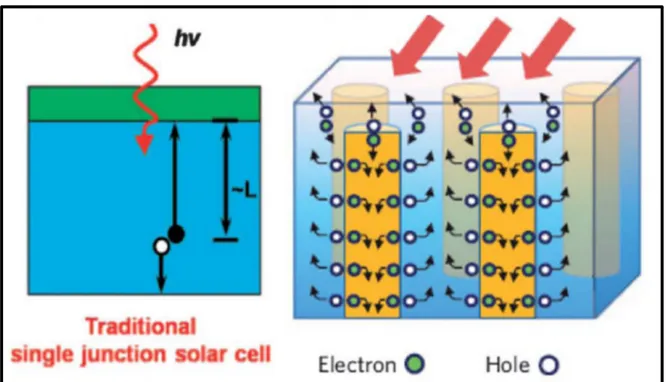
Junction formation is carried out to separate the photo generated electrons and holes after the synthesis of nanowires. Junction in a solar cell can be of two types: homojunction and heterojunction. Homojunction solar cells have similar semiconducting materials with equal band gaps but different doping concentrations. These types of solar cells can have single pn junction or pin junction or pnn+ or npp+ or any other junction combination consisting of different doping concentrations (Tawada, Okamoto et Hamakawa, 1981). Figure 3.3 (left) illustrates traditional single junction solar cell (Yu et al., 2012). On the other hand, heterojunction solar cells are composed of semiconductors of different band gaps. These kinds of solar cells have some advantages over homojunction solar cells. Since, these cells consist of different semiconducting materials, tuning into different bandgaps can enhance the wavelength response of the solar cell. However, it is hard to find semiconductors which have good lattice matching to obtain heterojunction solar cells. Three dimensional nanowire solar cells have been proposed by Fan et. al. (Fan et al., 2009) as shown in figure 3.3 (right), where the pn junction interface and light absorption direction are parallel to each other so that carrier collection takes place at perpendicular direction to the absorption of light. Using these nanowire structures, the pn junction interface area is increased compared with the planar
solar cells. Hence, minority carrier diffusion length is shortened which reduces the recombination loss of electrons.
Figure 3.3 Traditional single junction solar cell (left) Taken from (Yu et al., 2012)
3D nanowire solar cell (right) Taken from (Fan et al., 2009)
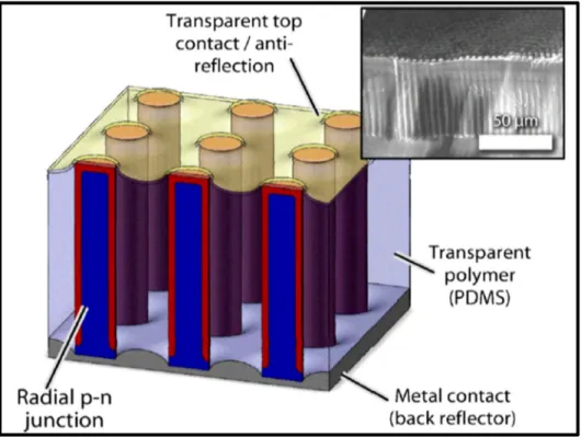
Electron hole pairs can be separated either in the radial direction or in the axial direction. Figure 3.4 depicts radial pn junction Si nanowire array solar cell geometry (Kelzenberg et al., 2009). Junction can be formed by epitaxial growth, diffusion and ion implantation. Among them, diffusion of impurities is a popular method used for doping in semiconductors. Nanowire heterojunctions can be fabricated using a thin film layer deposition on the top of the nanowire array by thermal evaporation, chemical vapor deposition, and pulsed laser deposition for inorganic materials. In case of organic materials and dye sensitized solar cells (Law et al., 2006), spin coating, dip coating, solution dye absorption is used.
Figure 3.4 Radial pn junction Si wire array solar cell geometry Inset SEM image of polymer embodied Si NW array
Taken from (Kelzenberg et al., 2009)
TiO2 is a wide bandgap, n-type semiconducting material in its anatase crystalline form (Forro
et al., 1994). Amorphous TiO2 can easily be synthesized using sol-gel technique by all
solution based method (Antonelli et Ying, 1995). Sintering at high temperature is used to prepare anatase crystalline TiO2 (Campostrini et al., 1994). Anatase TiO2 can be a potential
element to fabricate heterojunction with Si [ref]. It is useful to improve the optical and electrical characteristics of Si-based devices (Hwang, Boukai et Yang, 2009). Anatase TiO2
layer can be deposited on Si substrates via spin coating or dip coating processes (Wang, Helmersson et Käll, 2002).
Si-based hybrid heterojunction can also be formed using organic materials (Avasthi et al., 2011). Poly (3,4-ethelenedioxythiophene): poly (styrenesulfonate) (PEDOT:PSS) is an organic material that attracts a lot of attention now-a-days to fabricate efficient hybrid heterojunction with crystalline Si (Shen et al., 2011). Efficiency up to 16% has been reported by researchers for these types of hybrid heterojunction solar cells (Um et al., 2017). The
PEDOT:PSS layer can be employed as the hole transporting material for hybrid heterojunction solar cells (Sheng et al., 2016). PEDOT:PSS can be deposited on Si substrates using spin coating or dip coating methods (Subramani et al., 2016).
Implementing surface plasmon resonance (SPR) effect into silicon nanowire based solar cells helps to suppress the reflection in their resonance wavelength region (Anatoly et Igor, 2003). Adding minute amounts of silver nanoparticles in the silicon nanowires helps to achieve the plasmonic effect. These metallic nanoparticles interact with the incident light and scattered them in many directions. This phenomenon allows the solar cells to absorb more light since the scattered light travel along the solar cells.
Contacts are made to collect electrons and holes after formation of junctions in solar cells (Garnett et al., 2011). One of the contacts either top or bottom must be transparent for passing the light through it and the other one is made highly reflective for trapping and directing the light. The open circuit voltage, fill factor, short circuit current density and overall energy conversion efficiency are maximized if the contacts are ohmic (He et al., 2012) in nature. If the junction is Schottky type (Li et al., 2010), then one of the contacts has to be ohmic in nature and the other is Schottky. There are various ways of making the contacts, for instance in planar solar cells, ohmic contact is made by heavy doping of the nanowire system (Tress et al., 2011). The contact patterns are formed by either metal evaporation using mask or by writing the pattern using e-beam and photolithography (Garnett et al., 2011). These methods are generally employed for planar solar cells. Multiple lithography and etch step are required in case of radial junction based solar cells (Lu et Lal, 2010). For backside contact generally Ni/Al or Au is used and for the top contact grid Ag or Au is used(Garnett et al., 2011).
To conclude, this literature review section tried to give an overview of the synthesis of vertically aligned SiNWs and its potential applications in fabricating heterojunction solar cells, to develop a cost-effective way to produce third generation PV devices.
SIMULATION WORKS TO DETERMINE THE OPTICAL PROPERTIES OF THE SILICON NANOWIRES
4.1 Introduction:
The maximum theoretical efficiency of a single p-n junction solar cell was first theoretically calculated by William Shockley and Hans Queisser in 1961 (Shockley et Queisser, 1961). This limit also called detailed balance limit. According to this limit, the maximum theoretical efficiency is 33.7%. The main objective of the simulation part of this thesis is to check whether an ideal p-n junction that made using silicon nanowires could approach to the Shockley-Queisser limit. Hence, the loss mechanisms of light incident on the nanowire surface have to be understood properly.
4.2 Design of the modelling:
First, optical properties of silicon nanowires such as reflectance, transmittance and absorbance will be simulated using the Photonics SHA 2D tool (Ni et al., 2009). Photonics SHA 2D tool is used for modelling the optical parameters such as reflectance, transmittance, and absorbance using 2D spatial harmonic analysis method which is similar to RCWA of single period multilayer grating. In this tool the incident wave can be any plane electromagnetic wave with any incident angle. The incident wave can be TE or TM polarized wave. The solver of this tool was made of C with LAPACK. Then the ultimate photovoltaic efficiency of the nanowire solar cell will be calculated using this relation:
∞ = 0 0 ) ( ) ( ) ( λ λ λ λλ λ λ η λ d I d A I g g (4.1)η is the ultimate photovoltaic efficiency, A(λ) is the absorbance given by the equation ) ( ) ( 1 ) (λ R λ T λ A = − − ) (λ
R is the reflectance and T(λ) is the transmittance.
∞ 0
) (λ dλ
I is the solar irradiance spectra.
We have simulated the optical properties of the silicon nanowires having a fixed diameter of 100nm and verying the length of the nanowires from 300 nm to 1 µm. The simulation results have been shown in the next section.
4.3 Results:
Figure 4.1 Upper Image: Model geometry uses for SHA 2D tool (region in red color is air, green colored region is silicon nanowire and blue region is the silicon substrate) Lower Image: Optical properties vs. wavelength plot in 3 nm spacing (length of the nanowire
400nm and diameter 100nm)
Figure 4.1 and 4.2 represents the optical properties vs. wavelength plot for nanowires with lengths 400nm and 1 µm respectively.
Figure 4.2 Optical properties vs. wavelength plot in 3 nm spacing (length of the nanowire 1µm and diameter 100nm)
Table 4.1 Calculated solar cells efficiencies
Nanowire Length in nm Simulation spacing in nm Ultimate Photovoltaic Efficiency in %
400 3 24.6626
1000 3 29.25
4.4 Conclusion:
Longer nanowires are able to supress the reflection better than the shorter nanowires. Nanowire based solar cells have the ability to approach to the Shockley-Queisser limit if we can find the proper geometry (length, diameter, filling factor etc.) for these silicon nanowires.
PHONON PROCESSES IN VERTICALLY-ALIGNED SILICON NANOWIRE ARRAYS PRODUCED BY LOW-COST ALL-SOLUTION GALVANIC
DISPLACEMENT METHOD
D. Banerjee a, S. Cloutier b, C. Trudeau c and F. Gerlein d ,
a, b, c and d Department of Electrical Engineering, École de Technologie Supérieure,
1100 Notre-Dame West, Montreal, Quebec, Canada H3C 1K3 Paper published in Applied Physics Letters, March 2016
Abstract: The nanoscale engineering of silicon can change significantly its bulk
optoelectronic properties to make it more favorable for device integration. Phonon process engineering is one way to enhance inter-band transitions in silicon’s indirect band structure alignment. This paper demonstrates phonon localization at the tip of silicon nanowires fabricated by galvanic displacement using wet electroless chemical etching of a bulk silicon wafer. High-resolution Raman micro-spectroscopy reveals that such arrayed structures of silicon nanowires display phonon localization behaviors, which could help their integration into the future generations of nano-engineered silicon nanowire-based devices such as photodetectors and solar cells.
5.1 Introduction :
In recent years, significant efforts have provided a much better understanding of the unique electrical, mechanical and thermal properties of 1-dimensional nanostructures (Schmidt et al., 2009). Typically, nanowires have diameters on the order of few nanometers and lengths of hundreds of nanometers or more, favoring charge carrier transport along a single dimension. Silicon-based nanowires have become popular given the raw material’s availability, biocompatibility and low processing costs using current microelectronic standards. To fully exploit these advantageous material properties, the industry requires processes to fabricate silicon nanowire-based devices at low costs.
To date, different fabrication methods have produced silicon nanowires, including chemical vapor deposition using the vapor-liquid-solid technique (Westwater et al., 1997), laser