HAL Id: hal-01240772
https://hal-univ-rennes1.archives-ouvertes.fr/hal-01240772
Submitted on 22 Jan 2016
HAL is a multi-disciplinary open access
archive for the deposit and dissemination of
sci-entific research documents, whether they are
pub-lished or not. The documents may come from
teaching and research institutions in France or
abroad, or from public or private research centers.
L’archive ouverte pluridisciplinaire HAL, est
destinée au dépôt et à la diffusion de documents
scientifiques de niveau recherche, publiés ou non,
émanant des établissements d’enseignement et de
recherche français ou étrangers, des laboratoires
publics ou privés.
Brice Le Borgne, Anne-Claire Salaün, Laurent Pichon
To cite this version:
Brice Le Borgne, Anne-Claire Salaün, Laurent Pichon. Electrical properties of self-aligned
gate-all-around polycrystalline silicon nanowires field effect transistors. Microelectronic Engineering, Elsevier,
2016, 150, pp.32-38. �10.1016/j.mee.2015.11.001�. �hal-01240772�
ACCEPTED MANUSCRIPT
Electrical properties of self-aligned gate-all-around
polycrystalline silicon nanowires field effect transistors
Brice Le Borgne*, Anne-Claire Salaün* and Laurent Pichon*
*Microelectronics and Microsensors Department, Université de Rennes 1, Rennes, France
brice.leborgne@univ-rennes1.fr ; anne-claire.salaun@univ-rennes1.fr ;
laurent.pichon@univ-rennes1.fr
Abstract
Low temperature (≤ 600°C) polycrystalline silicon nanowires field effect transistors have been developed following a top down approach and classical photolithography techniques. N channel transistors have been tested with a single top-gate, bottom-gate and gate-all-around architecture in order to compare their electrical performances in relation to the interface state density. Analysis shows that surrounding gate enables control of parameters such as on-current, subthreshold slope and threshold voltage and offer potential further applications.
Keywords : gate-all-around, MOSFET, polycrystalline silicon, Si-nanowires, CMOS technology.
1.
Introduction
As integrating smaller sized high performance electronic devices has become a key point over the past decades, innovative transistor designs have emerged. Chip-to-wafer density has to remain high to be competitive so size reduction is still a burning issue and non-planar devices are part of these brand new products. As a consequence, multigate field effect transistors (FET) have been developed [1]. Dual Gate (DG) [2], tri-gate [3], FinFET [4] and Gate-All-Around (GAA) FET [5-7] are the main structures, based on various materials, described in literature and available on the market. In such new gate architecture passing from 2D to 3D, silicon nanowires (SiNWs) FETs seem to be one of the most attractive choices. They enable to avoid problems due to short channel effect such as threshold voltage (VTH) “roll-off” [8] or drain induced barrier lowering (DIBL) [9].
ACCEPTED MANUSCRIPT
More precisely, surrounding-gate transistors where the gate circles the nanowire channel allow a better electrostatic gate control. SiNWs can be prepared by a bottom-up method like layer by layer self-assembly [10], vapor-liquid-solid growth techniques [11], plasma-enhanced chemical vapor deposition (PECVD) [12] or using matrix template [13]. Nevertheless, the silicon nanowire growth process for device integration remains difficult as their size and positioning cannot always be perfectly controlled. In addition, SiNWs need to be selectively collected and handled in a planar layout. Most recent methods such as roll-to-roll technique enable SiNWs printing in order to obtain desired shapes and structures [14].
Top-down approach favors patterning architectures in a planar layout, most of the SiNWs are patterned on silicon-on-insulator substrates (SOI) by etching the first silicon layer down to buried oxide [15] because it provides best electrical performances for SiNW based FETs but the main drawback remains the high cost of these substrates. Several nano patterning techniques such as e-beam [16], atomic force microscopy [17] or deep-UV [18] were developed to achieve SiNWs. These high cost fabrication methods are not compatible with mass production. However, polycrystalline silicon SiNWs (poly-SiNWs) synthesis using sidewall spacer top down method [19-21] seems to be a lower cost alternative, fully compatible with planar complementary metal oxide semiconductor (CMOS) silicon technology.
Moreover, SiNWs FETs have nowadays attracted a lot of attention for the development of mechanical [22], biological [23] or chemical [24] sensors. In the latter two cases, SiNWs are used as sensitive units to detect charged chemical species, responsible for variation of the channel conductance. In particular, top-gate and back-gate transistors based on poly-SiNWs made by the spacer method showed to be good candidates to gas (ammonia) detection [25], pH sensing [26] and DNA hybridization [27].
GAA FETs are mainly known for enabling full channel depletion [6] so as to improve subthreshold slope (SS) and having low threshold voltage for identical subthreshold leakage current [28]. In addition, using double-gate devices proved interesting in relation to circuit drift compensation [29] because it allows dynamically fixing the threshold voltage as the second gate is able to control electrostatic effects (e.g. drift problems in organic light emitting diode (OLED) displays [30] or sensors [31]).
In this paper, we develop a low temperature (≤ 600°C) fabrication process of top-gate, bottom-gate and GAA FETs. SiNWs are made using the spacer method which is an original technique for GAA transistors fabrication. Independent biasing of each gate allows a possible threshold voltage control of these bottom gate (BGT) and top gate transistors (TGT). In addition, electrical connection of both bottom and top gate electrodes allows the formation of a gate that surrounds the channel, creating GAA architecture. Electrical performances are analyzed
ACCEPTED MANUSCRIPT
as a function of the density of state highlighting oxide/semiconducting nanowire interfaces difference in top and bottom gate configurations.
2.
Experimental
detailsPoly-SiNWs FETs are fabricated using a 4 masks and a CMOS compatible fabrication process. N-type transistors with parallel poly-SiNWs channels are fabricated using the sidewall spacer method described below, where the spacer at nano scale made of poly-Si constitutes the nanowire. The key nanowire fabrication steps are illustrated in Fig. 1 (not to scale). Substrate is firstly covered with a 1.2 μm thick silicon dioxide (SiO2)
insulating layer deposited by Atmospheric Pressure Chemical Vapor Deposition (APCVD) technique at 420°C (not shown). Then, a 750nm thick highly N-type in-situ doped amorphous silicon (a-Si) layer is deposited by Low Pressure Chemical Vapor Deposition (LPCVD) technique at 550°C with a silane/phosphine mixture at 900 μbar and crystallized by thermal annealing under vacuum at 600°C. This layer is then patterned to form step used as bottom gate using classical UV photolithography and etched by reactive ion etching. A 70 nm thick SiO2
gate insulator layer is then deposited by APCVD and densified by a thermal annealing at 600°C. Fig. 1(a) shows the obtained stepped bottom gate and the gate insulator layer. Then, a 750 nm thick LPCVD amorphous silicon layer, with two differently doped stacked regions is deposited and crystallized under the same conditions as bottom gate material. The 450 nm thick lower half layer is undoped and the 300 nm thick upper half layer is heavily N-type in-situ doped. This poly-Si layer is then patterned by plasma etching of this poly-Si layer to both create spacers (undoped) and source-drain electrodes (highly doped) of the transistor, as shown in Fig. 1(b). The channel length L is 5 μm and its widths (WTOP and WBOT) are 425 nm and 600 nm for top-gate and bottom-gate
configurations respectively. In this case, using the spacer method to form SiNWs avoid using another photomasking step as it is not necessary to form source and drain regions. This technique enables self-alignment of gate. This key fabrication step enables formation of several nanowires and cost reduction of the process. Thanks to the 500 patterned steps in the bottom gate, 1.000 nanowires are formed to allow a high current level in the transistor.
A second 70 nm thick SiO2 gate insulator is then deposited by the APCVD technique and densified. Then, a
300 nm thick N-type heavily in-situ doped silicon layer is deposited and crystallized. This layer is then etched to form the transistor’s top-gate as shown in Fig. 1(c). Fig. 1(d) presents a schematic and a SEM image of a cross section of the whole device in its final version.
ACCEPTED MANUSCRIPT
Polycrystalline SiNWs used as channel region are common for top and bottom gates transistors. In addition, both gates can be electrically tied to form a single surrounding gate, called Gate-All-Around (GAA) transistors. Using spacer method to fabricate these transistors was not done before. Fig. 2 presents a SEM view of the device after this final stage of the fabrication process. Static electrical characteristics of the devices are collected at room temperature using an Agilent B1500A semiconductor parameter analyzer.
3. Results and Discussions
3.1. Electrical measurement of bottom and top-gate SiNWFETs
Fig. 3 presents the device performance of a single bottom or top-gate transistor. The plotted characteristics are all drawn from the same transistor based on 1.000 SiNWs by biasing either top or bottom gates of the device. The average width of SiNWs is 300 nm. The BGT and TGT show an N-type field effect transistor enhancement. TGT exhibits higher electrical performances: a higher ION/IOFF ratio and SS, and a lower VTH as previously
reported [24]. These results are explained because quality of insulator/poly-SiNWs interface is better on the upper part of the nanowires than in the lower part. Indeed, for the BGT, channel region takes place in the seed layer of the poly-Si used to form nanowire with a higher defects density than the upper crystalline silicon nanowire surface. Thus, because the amorphous crystallization process begins at the SiO2/a-Si interface, the
defect density (including grain boundaries) is higher in the lower part of the poly-Si layer (a few nanometers thick) constituting the nanowires (see Fig. 4). These grain morphology and defect densities of Si-poly layers deposited in the same conditions were previously revealed by Haji et al [32] using transmission electron microscopy (TEM) analysis. These observations will be confirmed by electrical measurements of the interface state density in the section 3.2. Consequently, such defects lead to a poor electrode/channel interface quality because of the parasitic contact resistances. It could be due to the non-linear behavior of drain current at low source-drain voltages output characteristics for BGT compared to TGT (Fig. 5).
3.2. Electrical measurement of dual gate SiNWFETs
bottom-ACCEPTED MANUSCRIPT
gate voltages. Both measurements present N-type field-effect transistor enhancement with changes for off-state current values, threshold voltage and subthreshold slope. Values of VTH and SS are summed up in Fig. 7. We
note that for negative bottom-gate biasing, VGBot, (Fig. 5(a)), VTH, SS and on-current (ION) are quite similar,
about 12.6 V, 4.0 V/decade and 1.4 u 10-4 A respectively, which indicates a good stability of the transistor for
on-state mode. However off-current (IOFF) is bottom-gate dependent and increases as negative VGBot decreases.
Indeed, in usual off state mode the inversion (holes) canal is responsible for the low leakage current through the reverse biased PN+ junction at the drain. However, in our case, the negative bottom gate bias prevents the
inversion (holes) top channel formation due to a likely drive back of electrons in the top region for negative bottom gate bias, which promotes electrical conduction in the core of the active layer resulting in an IOFF
increasing. In contrast, Fig. 6(b) highlights a dependency of SS parameter, VTH and IOFF for high VGBot positive
values (>10V). In this case, VTH decreases (from 12.4 V to 3 V) and SS increases (from 3.3 V/dec to 8.7 V/dec)
as VGBot increases, resulting in a degradation of the on/off states switching of the TGT’s transfer characteristics.
For positive VGBot values, the electric field may be high enough to attract electrons in the lower part of the
nanowire. A channel is then formed in this region as VGTop increases, responsible for a “parasitic” conduction at
the back side of the SiNWs. Consequently, the TGT’s apparent VTH decreases as VGBot increases. In the
meantime, subthreshold slope increases with VGTop. These hypotheses are confirmed by numerical calculation of
carriers distribution within the poly-Si nanowires reported in the following section.
The numerical modeling of the dual-gate MOS structure (Top gate/Top oxide/Silicon Nanowires/Bottom oxide/Bottom gate) which is the basic vertical structure of the transistor (Fig. 8) is performed to highlight these effects of the voltage gates and of defects through the response of carrier concentration in the channel. This modelling solves the Poisson equation in order to calculate the electrostatic potential variation induced by an applied voltage. The finite element method is used to solve the Poisson equation in an iterative scheme in order to calculate the electrostatic potential, calculated at all the mesh points.
Our calculation illustrates tendencies of the conduction behaviors at VTH = 0 V. The polycrystalline silicon is
formed by crystallites composed of grains (considered as single crystal silicon), separated by grain boundaries, highly disordered and very narrow areas, of the order of several nanometers thick. This separation between two grains is considered as an amorphous silicon layer, and we use a model distribution of traps [34], taking into account the dangling bonds, tails bands and discrete traps. The mesh is very tight near the grain boundaries because of strong potential variations near grain boundaries. Moreover, modelling takes into account all the physical parameters characterizing the structure: thickness of the various layers, permittivity, work output,
ACCEPTED MANUSCRIPT
silicon doping. Results are reported in Fig. 9. From these simulation’s results, one can suggest that at positive constant top-gate biasing, as long as bottom-gate biasing remains at negative or low positive values, the lower part of the nanowire is depleted. When a high positive value is reached, simulation results highlight an increase of the electrons concentration in the lower part of the nanowires, suggesting the formation of electron channel conduction in its lower part. In this case, one can consider that conduction in the lower part of the nanowire is not negligible anymore. Similarly, Fig. 9(b) points out that high negative bias values generate a channel of holes in the lower part of the poly-SiNW.
Our measurements show a relative stability of the transistor for VGBot < 10 V. For higher VGBOT values the
TGT's threshold voltage can be modulated (Fig. 7). This VTH control can offer many potential applications for
circuit drift compensation such as OLED displays or sensors. The counterpart of this dual-gate poly-SiNWs FET main advantage is degradation of SS parameters and ION/IOFF ratio. Nevertheless, for a drift compensation for the
previously mentioned applications, high electrical performances in terms of high subthreshold switching are not necessarily desired.
3.3. Electrical measurement of GAA SiNWFET
Fig. 10 presents poly-SiNWs GAA FET electrical performances. Transfer characteristic at VDS = 3 V (Fig.
10(a)) shows an N-type enhancement and main electrical parameters are VTH = 13.4 V, SS = 2.3 V/dec and
on-state current value similar to previous gate bias configuration of the device. We note that no rectifying behavior in the linear mode is observed as for BGT working mode (Fig. 10(b)). This means that bottom channel conduction does not dominate when bias is applied on the surrounding gate. The ION/IOFF ratio is significantly
higher than TGT’s which may be due to a likely full depletion of charge carriers in the core of the poly-SiNWs in the GAA working mode (for 4V < VG < 7V). The surrounding gate improves TGT’s performances in terms of
switching ratio.
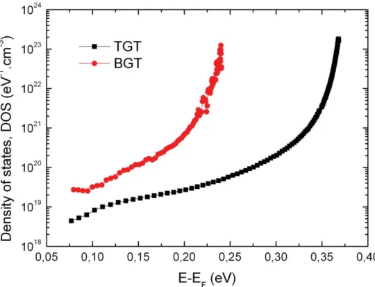
3.4. Density of states calculation
As mentioned previously, electrical properties of TGT, BGT and GAA transistor are strongly dependent on the interface and active layer qualities. In this way, we calculated density of states (DOS) in the poly- SiNWs based
ACCEPTED MANUSCRIPT
TGT and BGT. Such evaluations give information about quality of the material at the upper and the lower parts of the nanowires. As poly-Si is the active material, DOS estimation was done using the field-effect based Suzuki’s incremental method [34]. Fig. 11 shows DOS values for these two transistors architectures. One can notice that BGT has a higher DOS than TGT. In particular, DOS is significantly higher (more than one decade) for high levels into the bandgap (related to tail states). One can consider that DOS is closely linked to oxide/polycrystalline silicon interface state because the conduction channel is mainly formed at this interface, in first few nanometers of the nanowire. It confirms the lower interface quality at the bottom part of SiNWs compared to its upper part. In other words, the upper part of the nanowires is better quality than lower part, which was supposed in a previous study [35]. In addition, these results confirm that in the GAA configuration, channel could be formed preferably in the upper region of SiNWs and leading to similar electrical characteristics for TGT configuration.
4.
Conclusion
Polycrystalline silicon nanowire based field effect transistor has been fabricated by low-cost classical CMOS techniques. This transistor enabled top-gate, bottom-gate, dual-gate or gate-all-around configurations testing. The threshold voltage and subthreshold slope of top-gate transistor showed stability whereas the bottom-gate one was unsettled by contact resistances. In dual-gate configuration, properties show electrical stability for low positive bottom-gate biasing. Positive bottom-gate biasing induces formation of a bottom channel as defects participate to electrical conduction under some conditions which has been confirmed by simulation results. These transistors require very high operating voltages due to poor interface and crystalline quality of the material. Density of states calculations seem to confirm this hypothesis. Such a study can be a method to analyse nanowires based devices. Nevertheless, low operating voltage is not a key requirement for sensing applications. Further study on crystallization process of the polycrystalline silicon nanowire to reduce the crystal defect density could offer potential applications for low voltages electronic functions based on such transistors. In dual-gate mode, transistor enables a VTH control thanks to the bottom-gate. Such a control can find application for
sensors and OLED displays drift compensation. Gate-all-around architecture present characteristics related to top-gate configuration with better switching properties. In addition, as reported in previous works, poly-SiNWs based devices can be used for species detection, therefore the feasibility of such GAA structures and the
ACCEPTED MANUSCRIPT
potential effects of charged species on the SiNWs conductance in this configuration could benefit for the fabrication of high performance biochemical sensors.
References
[1]
H.H. Hsu, T.W. Liu, L. Chan, C.D. Lin, T.Y. Huang, H.C. Lin, IEEE Trans. Electron Devices
55 (2008) 3063.
[2]
S. Kim, J. Nah, I. Jo, D. Shahrjerdi, L. Colombo, Z. Yao, E. Tutuc, S.K. Banerjee, Appl. Phys.
Lett. 94 (062107) (2009).
[3]
B. Doyle, S. Datta, M. Doczy, S. Hareland, B. Jin, J. Kavalieros, T. Linton, A. Murthy, R.
Rios and R. Chau, IEEE Electron Device Lett. 24 (2003) 263.
[4]
M. Zaborowski, D. Tomaszewski, A. Panas and P. Grabiec, Microelectronics Engineering 87
(2010) 1396.
[5]
J.P. Colinge, M.H. Gao, A. Romano-Rodriguez, M. Maes, C. Claeys,
IEEE IEDM'90 (1990)
595.
[6]
N. Singh, A. Agarwal, L.K Bera, T.Y. Liow, R. Yang, S.C. Rustagi, D.L. Kwong, IEEE
Electron Device Lett. 27 (2006) 383.
[7]
K. Nayak, M. Bajaj, A. Konar, P.J. Oldiges, K. Natori, H. Iwai, K.V.R.M. Murali, V.
Ramgopal Rao, IEEE Trans. Electron Devices 61 (2014) 3066.
[8]
H. Abd-Elhamid, B. Iniguez, D. Jimenez, J. Roig, J. Pallarès, L.F. Marsal, Solid-State
Electron. 50 (2006) 805.
[9]
M. Jagadesh Kumar, V. Verma, IEEE Trans. Reliab. 51 (2002) 367.
ACCEPTED MANUSCRIPT
[11]
J. Westwater, D.P. Gosain, S. Tomiya, S. Usui, H. Ruda, J. Vac. Sci. Technol. B 15 (1997)
554.
[12]
M. Cuscunà, A. Convertino, L. Mariucci, G. Fortunato, L. Felisari, G. Nicotra, C. Spinella, A.
Pecora, F. Martelli, Nanotechnology 21 (255601) (2010).
[13]
R. Fan, Y. Wu, D. Li, M. Yue, A. Majumdar, P. Yang, J. Am. Chem. Soc. 125 (2003) 5254.
[14] R. Yerushalmi, Z.A. Jacobson, J.C. Ho, Z. Fan, A. Javey, Appl. Phys. Lett. 91 (203104)
(2007).
[15] N.A. Melosh, A. Boukai, F. Diana, B. Gerardot, A. Badolato, P.M. Petroff, J.R. Heath,
Science 300 (2003) 112.
[16]
B. Tian, X. Zheng, T.J. Kempa, Y. Fang, N. Yu, G. Yu, J. Huang, C.M. Lieber, Nature 449
(2007) 885.
[17]
S. Hu, A. Hamidi, S. Altmeyer, T. Köster, B. Spangenberg, H. Kurz, J. Vac. Sci. Technol. 16
(1998) 2822.
[18]
C.T. Black, Appl. Phys. Lett. 87 (163116 ) (2005).
[19]
F. Demami, L. Ni, R. Rogel, A.C. Salaün, L. Pichon, Sensor. Actuat. B-Chem. 170 (2012)
158.
[20]
I. Amit, D. Englander, D. Horvitz, Y. Sasson, Y. Rosenwaks, Nano Lett. 14 (2014) 6190.
[21]
H.C. Lin, C.J. Su, IEEE T. Nanotechnol. 6 (2007) 206.
[22]
L. Lou, S. Zhang, W.T. Park, J.M. Tsai, D.L. Kwong, C. Lee, J. Micromech. Microeng. 22
(055012) (2012).
[23]
G. Wenga, E. Jacques, A.C. SalaünC, R. Rogel, L. Pichon, F. Geneste, Procedia engineering
47 (2012) 414.
[24]
L. Ni, E. Jacques, R. Rogel, A.C. Salaün, L. Pichon, G. Wenga, Procedia engineering 47
(2012) 240.
ACCEPTED MANUSCRIPT
[25]
R. Rogel, E. Jacques, L. Pichon, A.C. Salaün, IEEE Trans. Electron. Devices 61 (2014) 598.
[26]
Y. Cui, Q. Wei, H. Park, C.M. Lieber, Science 293 (2001) 1289.
[27]
G. Godem, E. Jacques, A.C. Salaün, R. Rogel, L. Pichon, F. Geneste, Biosensors (2012) 1.
[28]
M. Jamal Deen, T. A. Fjeldly, CMOS RF Modeling, Characterization and Applications (2002)
1188
[29]
K. Kandoussi, E. Jacques, N. Coulon, C. Simon, T. Mohammed-Brahim, Solid-State Electron.
63 (2014) 140.
[30]
J. Boizot, V. Gohri and H. Doyeux, MRS Proceedings (2011) 1359.
[31]
A. Vergara, S. Vembu, T. Ayhan, M.A. Ryan, M.L. Homer, R. Huerta, Sensor. Actuat.
B-Chem. 166 (2012) 320.
[32]
L. Haji, P. Joubert, J. Stoemenos, N.A. Economou, J. Appl. Phys. 75 (1994) 3944.
[33]
C.A. Dimitriadis, J. Appl. Phys. 73 (1993) 4086.
[34]
T. Suzuki, Y. Osaka, M. Hirose, Japanese Journal of Applied Physics 21 (1982) 159.
ACCEPTED MANUSCRIPT
Fig. 1. Gate-All-Around Field-Effect Transistor fabrication steps: (a) stepped bottom-gate patterning and bottom oxide layer deposition, (b) polycrystalline silicon nanowire channel and drain-source zone formation and SEM image, (c) top-gate formation and (d) cross section of the final device with main dimensions : L = 5 μm, WTOP =
ACCEPTED MANUSCRIPT
Fig. 2. (a) SEM imaging of the device with drain-source zone, multiple parallel polycrystalline silicon nanowires channels, bottom-and top-gate main regions and (b) schematic detailed view of this SEM image.
Fig. 3. Transfer characteristics of poly-Si NWFET IDS–VGS: (a) bottom-gate and (b) top-gate transistors (1000
ACCEPTED MANUSCRIPT
(a)
(b)
Fig. 4. Schematic cross section view illustrating the columnar type structure of a polycristalline silicon layer (a). Size lowering leads to a higher defects density within the polycristalline SiNWs close to the Si nanostructure/SiO2 interface (b)
Fig. 5. Output characteristics of poly-Si NWFET ID–VDS: (a) bottom-gate and (b) top-gate transistors (1000
nanowires, L=5 μm). Measurement step is 2V. Saturation mode is easily reached for TGT and is not reached for BGT.
ACCEPTED MANUSCRIPT
Fig. 6. Transfer characteristics of the top gate poly-Si NWFET ID–VGTop: (a) bottom-gate negative biasing and
(b) positive biasing (VDS = 3 V). These plots show a VGBot sign dependence behavior, due to formation of a
bottom channel.
Fig. 7. Bottom-gate bias effect on subthreshold slope and threshold voltage on poly-SiNWs FET with separated top and bottom-gate electrodes (VDS = 3 V). A relative stability of device is observed for VGBot < 10 V.
ACCEPTED MANUSCRIPT
Fig. 8. Schematic structure of nanowires composed of 5 monocrystalline grains (width 80nm) and 4 amorphous grain boundary (a) (2.5 nm thickness), with a 80nm gate oxide thickness and cross section of final GAA structure (b).
Fig. 9. Simulated distribution of electrons (a) at VTop=1V (VGBot =-0.5 to 1V) and holes (b) through a 300 nm
ACCEPTED MANUSCRIPT
Fig. 10. Gate-All-Around poly-Si NWFET transfer ID-VG (a) and output ID-VDS (b) characteristics, showing a
ACCEPTED MANUSCRIPT
Fig. 11. Density of states for top, and bottom transistors configurations determined by Suzuki’s method. Bottom-gate transistor shows higher DOS values than other two architectures.