This is an author-deposited version published in:
http://oatao.univ-toulouse.fr/
Eprints ID: 5066
To link to this article: DOI:10.1109/TNS.2011.2171005
URL:
http://dx.doi.org/10.1109/TNS.2011.2171005
To cite this version:
Virmontois, Cédric and Goiffon, Vincent and
Magnan, Pierre and Saint-Pé, Olivier and Girard, Sylvain and Petit, Sophie
and Rolland, Guy and Bardoux, Alain Total ionizing dose versus
displacement damage dose induced dark current random telegraph signals
in CMOS image sensors. (2011) IEEE Transactions on Nuclear Science,
vol. 58 (n° 6). pp. 3085-3094. ISSN 0018-9499
O
pen
A
rchive
T
oulouse
A
rchive
O
uverte (
OATAO
)
OATAO is an open access repository that collects the work of Toulouse researchers and
makes it freely available over the web where possible.
Any correspondence concerning this service should be sent to the repository
administrator:
[email protected]
1
Total Ionizing Dose Versus Displacement Damage
Dose Induced Dark Current Random Telegraph
Signals in CMOS Image Sensors
Cedric Virmontois, Student Member, IEEE, V. Goiffon, Member, IEEE, P. Magnan, Member, IEEE, O. Saint-Pé,
S. Girard, Member, IEEE, S. Petit, G. Rolland, and A. Bardoux
Abstract—Dark current Random Telegraph Signals due to total
ionizing dose (TID) and displacement damage dose (DDD) are in-vestigated in CMOS image sensors. Discrepancies between both RTS are emphasised to better understand the microscopic origins of the phenomena.
Index Terms—Active pixel sensor (APS), CMOS image sensor
(CIS), displacement damage dose (DDD), hot pixels, monolithic ac-tive pixel sensor (MAPS), random telegraph signal RTS), total ion-izing dose (TID).
I. INTRODUCTION
S
PACE applications require integrated circuits able to op-erate in the harsh environment associated with the mis-sions. For Active Pixel Sensor (APS), also called CMOS Image Sensor (CIS), a key issue is the mean dark current increase with the total radiation dose [1]. Radiation effect studies also showed a discrete fluctuation of the dark current after irradiation, re-ferred to as random telegraph signal (RTS) [2].Two types of RTS are known to occur in CIS and their source locations are shown in Fig. 1. The first corresponds to an increase of the sensor temporal readout noise due to the discrete fluctuations of the in-pixel Source Follower (SF) channel conductance [3]–[5]. It is explained by carrier trapping and emission by oxide traps located in the MOSFET channel, and hence is referred to as MOSFET-RTS or SF-RTS in CIS. The second type of RTS is a discrete variation of the photo-diode dark current (DC-RTS) [6]–[13]. It is due to meta-stable Shockley–Read–Hall (SRH) Recombination-Generation (R-G) centers located inside the Space Charge Region (SCR) of the photodiode. It is well established that, in the case of displace-ment damages, the DC-RTS centers are located in the silicon bulk [2]. It has also been demonstrated [6] that total ionizing dose can generate meta-stable SRH R-G centers at the Si/SiO interfaces that can lead to DC-RTS in CIS.
Manuscript received July 22, 2011; revised September 09, 2011; accepted September 27, 2011. This work was supported in part by EADS Astrium and CNES
C. Virmontois, V. Goiffon, and P. Magnan are with the Université de Toulouse, ISAE, 31055 Toulouse, France (e-mail: [email protected]).
O. Saint-Pé is with EADS Astrium, 31402 Toulouse, France. S. Girard is with CEA, DAM, DIF, F91297 Arpajon, France.
S. Petit, G. Rolland, and A. Bardoux are with CNES, 31401 Toulouse, France. Color versions of one or more of the figures in this paper are available online at http://ieeexplore.ieee.org.
Digital Object Identifier 10.1109/TNS.2011.2171005
Fig. 1. Schematic diagram of 3T pixel unit cell. The locations of the two types of parasitic RTS are presented. The DC-RTS has an impact on the photodiode leakage current and the MOSFET-RTS (or SF-RTS) changes the channel con-ductance of the source follower transistor.
SF-RTS is independent of integration time whereas the dark signal voltage variation induced by the dark current is proportional to the integration time. Therefore, the two types of RTS can be easily distinguished by varying the integration time. Fig. 2 illustrates a DC-RTS signal for several integration times associated with a sensor irradiated with neutrons which induced displacement damages in the silicon lattice. The RTS amplitude is proportional to integration time proving that the observed RTS corresponds to DC-RTS. The RTS amplitudes observed before irradiation and after X and -rays exposures are also proportional to integration time [6]. These results confirm that the RTS studied here is a DC-RTS as opposed to SF-RTS [3]–[5]. Further evidences that the RTS observed in this work is not SF-RTS is given by the DC-RTS time constants that are more than two orders of magnitude longer than the slowest source of SF-RTS than can pass through the high pass non correlated double sampling filter [6].
The dark current RTS (DC-RTS) has been studied in image sensors for several years [5]–[13] and has been shown to strongly impact the calibration of detector for space missions. It is generally accepted that these temporal fluctuations are due to random changes in the generation-recombination current caused by charge or structural changes of complex defects located inside the depleted volume of the in-pixel photodiode. From proton irradiation tests, previous workers suggested that the number of generated DC-RTS centers scales with elastic non-ionizing energy loss (NIEL) [2], [7], or with total (elastic
Fig. 2. DC-RTS of pixel [28, 28] from IC 3. Amplitude of DC-RTS is propor-tional to the integration time. IC 3 was irradiated with 14 MeV neutron and the DDD reached 39 TeV/g. The device IC 3 is defined in Table I.
TABLE I
IRRADIATIONCHARACTERISTICS
plus inelastic) NIEL (i.e., proportional to displacement damage dose (DDD)) [8], [12]. In [9], the authors showed that total ionizing dose (TID) deposited by protons cannot be responsible for the reported fluctuations. This means that these DC-RTS defects are R-G SRH centers located in the silicon bulk and more precisely are not located at the Si/SiO interfaces. Elec-tric field enhancement (EFE) [14] was assumed to play a role in DC-RTS phenomenon [9]. In this hypothesis, the defects responsible for DC-RTS are supposed to be located in high electric field region where the magnitude of the electric field leads to an enhancement of the defect generation rate. Another possible explanation is the transfer of charges between defects from the same cluster [15].
In [12], an unexplained distribution peak, influenced by the proton fluence, was observed on the amplitude distribution of DC-RTS. It has been shown more recently that this peak was due to TID induced DC-RTS at the oxide interface [6]. This latter DC-RTS is associated with a meta-stable SRH R-G mechanism [16] at oxide interfaces, mainly located at the trench isolation interfaces. This means that different types of defects can lead to DC-RTS in the same pixel. Fig. 3 presents the temporal fluctu-ations of the dark current showing DC-RTS behavior. The phe-nomenon could happen either before irradiation (purple signal, IC1), after X and -ray irradiations (ionizing effect; red signal, IC 1) or after neutron irradiations (displacement damage effect; blue signal, IC 3). In CIS, TID creates energy states located at the trench isolation interface with silicon, whereas DDD gen-erates bulk defects in silicon. Both types of defects can be lo-cated inside the space charge region of the in-pixel photodiode, as shown in Fig. 4, and may act as meta-stable SRH R-G centers resulting in DC-RTS.
Fig. 3. Temporal representations of dark current showing DC RTS before irra-diation and after 10 keV X-ray and 14 MeV neutron irrairra-diations. Devices IC 1, 3 are standard layout and reference in Table I.
Fig. 4. Cross section of in-pixel photodiode. Blue dashed line represents space charge region (SCR). The defects, induced by TID and DDD, responsible for DC-RTS are represented in the cross section: Blue circles represent active DC-RTS bulk defects and red crosses represent active DC-RTS interface states.
In this paper, we study and compare the dark current RTS due to displacement damage dose ( ) and to total ionizing dose ( ) in CIS processed in deep sub-micron technology. In order to separate both effects, neutron and X/ -ray irradiations are carried out to differentiate between the displacement damage and total ionizing dose contributions to DC-RTS. Proton irradiations that produce both TID and DDD are also performed to observe the accumulation of both DC-RTS types. First, we present the specific characteristics used to describe DC-RTS, and its evolution with TID and DDD. The investigated RTS parameters are the number of levels, the maximum amplitudes and the switching time constants be-tween levels. Then, the origins of DC-RTS are discussed thanks to measurements performed on CIS with design variations. Annealing behavior of the dark current and the DC-RTS pixels are explored to extend our knowledge of the defect mechanisms responsible for DC-RTS phenomena.
II. EXPERIMENTALDETAILS
The studied components are 10 m-pitch 128 128 pixel arrays with 3T-pixels. These circuits are manufactured in a 0.18 m commercial CIS process. Table I lists the 10 tested devices. Identical standard pixel arrays are called IC and the two other with design variations are called DV.
The DC-RTS is detected by an automated detection method. This method is detailed in [12] and relies on a classical edge
de-VIRMONTOIS et al.: TOTAL IONIZING DOSE VERSUS DISPLACEMENT DAMAGE DOSE INDUCED DARK CURRENT RANDOM TELEGRAPH SIGNALS 3
Fig. 5. Mapping of detected DC-RTS pixel for several DDD (neutron irradiations) are illustrated at the first line of the figure whereas the mapping for several TID (X and -rays irradiations) are illustrated at the second line. , and . Pixel color represents the number of DC-RTS levels inside the pixel.
tection technique. The measured temporal dark current of one pixel is filtered by an edge detection digital filter. When a pixel exhibiting dark current fluctuation is detected, the algorithm de-termines the number and the values of the discrete dark current levels, the maximum transition amplitude and the number of transitions during the observation time. The entire pixel array is scanned to obtain the RTS characteristics of each individual pixel. The duration of the RTS measurement is 10 hours, and dark current values are recorded every 2 seconds for all tests. The output voltage range has been chosen to insure the linearity of dark signal with time. In this case, the dark current can be expressed as
(1) where is the average over 100 frames taken at min-imum integration time, ms. is the pixel output signal at time with an integration time . is measured every 2 seconds during the 10 hours experiment. CVF is the conversion to voltage factor including the readout chain gain. The dark current is referred to the readout node as illustrated in Fig. 1. An air oven was used to maintain the temperature at 22 C during measurements.
The sensors were exposed to neutron beams at Université Catholique de Louvain (UCL) facility and CEA DAM Valduc. Proton irradiations were realized at TRIUMF (Vancouver), at Kernfysisch Versneller Instituut (KVI) and at UCL. The X-ray tests were performed at CEA, DAM DIF. The -ray irradiations took place at UCL. The total DDD ranged from 34 to 365 TeV/g and the TID ranged from 3 to 300 Gy SiO . The irradiation
conditions for each sensor are provided in Table I. All irradia-tions were performed at room temperature.
Isochronal annealing with a 30-minute duration were per-formed between 80 C and 280 C with temperature steps of 40 C. After each annealing step, the sensor was brought to room temperature, and the dark current of each pixel in the array was measured and DC-RTS pixels were identified.
III. DARKCURRENTRTS (DC-RTS)
A. DC-RTS Pixel Number Evolution With Radiation Doses The mappings of detected DC-RTS pixels after exposure to neutrons, X and -rays are presented in Fig. 5. The number of detected DC-RTS pixels increases with both TID and DDD. The pixel color represents the number of DC-RTS levels in the in-dividual pixel. We can see that in neutron irradiated pixels with low DDD (39 TeV/g), a high number of RTS levels is present. It is not the case with TID, at low dose (3 Gy SiO ) A majority of pixels with two DC-RTS levels are present. It is important to no-tice that DC-RTS pixels observed before irradiation behave sim-ilarly to the ones detected after X and -rays, with the same av-erage number of levels. Fig. 6 emphasizes the number increase of pixels presenting DC-RTS with TID and DDD. Following TID, the percentage of detected DC-RTS pixels raises quickly, around 30% each 10 Gy SiO . The majority of the pixels ex-hibits DC-RTS behavior at approximately 20 Gy SiO . Above 20 Gy SiO , one can see that the curve starts to saturate. This can be explained by noting that the RTS detection threshold is increased due to the TID-induced increase of the shot noise that avoid detection of the DC-RTS pixels with low amplitudes. In
Fig. 6. Evolution of detected DC-RTS pixel percentage following DDD and TID. Both doses impact this percentage, a quick rise for TID and a proportional rise for DDD (14 and 22 MeV neutron irradiations). TID corresponds to X-rays irradiations under 30 Gy SiO and to -rays irradiations for 30 Gy SiO and above.
Fig. 7. DC-RTS number of level distribution after several DDD.
fact, once the TID level reaches 30–40 Gy SiO , almost every pixel in the array will have DC-RTS but this effect is masked by the dark current. Concerning DDD, the percentage of detected pixel rises proportionally, around 0.2% per TeV/g in the range from 0 to 365 TeV/g. This correlation confirms previous work conclusions on the proportionality number of DC-RTS pixels with the fluence and on total-NIEL [8], [12].
B. Number of Levels
The distributions of the number of levels per DC-RTS pixel are presented in Figs. 7 and 8 respectively after several DDD and several TID. Number of levels higher than two can be due to the contribution of either a sum of two or more 2-level DC-RTS centers, by one or more multi-level DC-RTS [12] centers or by the combination of both [13]. In Fig. 7, the highest number of detected levels (7 levels) is reached at the lowest DDD whereas in Fig. 8, the highest number of levels increases with TID. This suggests that TID induces more 2-level DC-RTS which accu-mulate at higher TID and are responsible for the higher number of levels. On the contrary, more multi-level DC-RTS seem to be created with DDD. By looking at the 365 TeV/g curve in Fig. 7 and the 300 Gy SiO curve in Fig. 8, no clear difference can be seen between TID and DDD induced DC-RTS. Therefore, the distribution of the number of RTS levels per pixel does not
Fig. 8. DC-RTS number of level distribution after several TID. TID corre-sponds to X-ray irradiations under 30 Gy SiO and to -rays irradiations for dose of 30 Gy SiO and above.
Fig. 9. DC-RTS example, obtained after 39 TeV/g neutron exposure, repre-senting transition maximum amplitude ( ) and peak to peak amplitude ( ) during one hour observation. In case of multi-level DC-RTS due to several meta-stable defects, peak to peak amplitude take into account several DC-RTS center whereas transition maximum amplitude observe only one defect.
appear to be an efficient tool to differentiate between the two DC-RTS related to DDD or TID.
C. DC-RTS Transition Maximum Amplitude
The maximum amplitude of DC-RTS transition is investi-gated for both TID and DDD exposures. This parameter corresponds to the maximal amplitude between two switching transitions, that is to say, the largest DC-RTS transition observed for each pixel signal. It is important to notice that this ampli-tude does not necessarily correspond to the peak-to-peak am-plitude ( ) between the highest and the lowest level of a DC-RTS as illustrated in Fig. 9.
Fig. 10 displays the statistical distribution of for every pixel of each tested sensor. DC-RTS due to DDD (neutron dis-tributions) shows larger amplitude than TID induced DC-RTS (X-rays and -rays distributions). Indeed, displacement damage induced amplitude larger than 8000 (up to 30000 in the total distribution which is not entirely plot for clarity pur-pose) whereas TID induced smaller amplitude and the max-imum stay under 2000 even at 300 Gy SiO . This point is the first way to differentiate between the two DC-RTS types. It is important to notice that the lowest amplitudes at the beginning of the distributions are not considered because they are impacted by the threshold of the detection method. This threshold is re-lated to the shot noise which increases with both radiation doses.
VIRMONTOIS et al.: TOTAL IONIZING DOSE VERSUS DISPLACEMENT DAMAGE DOSE INDUCED DARK CURRENT RANDOM TELEGRAPH SIGNALS 5
Fig. 10. DC-RTS transition maximum amplitude histogram. No irradiated de-vice and dede-vice exposed to TID (X and -rays) show weak amplitudes (under 2000 ) and the same exponential decrease behavior with around 110 . Devices exposed to DDD (14 and 22 MeV neutrons) show larger ampli-tude and typical exponential decrease behavior with around 1200 . Amplitude extreme values for maximum DDD go up to 30000 .
Therefore, the smaller amplitude is masked when the shot noise increased with doses (it explains the shape of the distribution in the first bins). The second way of differentiation is the ex-ponential decrease behavior of the distributions. Distributions could be fitted by a slope on the semi-log graph enabling the determination of parameter from the exponential behavior [(2)].
(2) where is the average of the law and a constant. The non-irradiated device and the devices exposed to different TID, show the same slope . The parameter induced is equal to 110 . DC-RTS before irradiation and after TID probably arises from the same meta-stable generation centers which are assumed to be interface states inside trench isolations surrounding in-pixel photodiode [6]. In this case, the parameter should be dependent on the type and quality of the trench isolation. Concerning devices exposed to DDD, the slope is not the same as the one obtained with TID. However, the slope remains identical at the different DDD increase leading to a parameter constant value around 1200 . This suggests a generic (i.e., independent on the particle type or energy) DC-RTS behavior of the bulk meta-stable defects inside the in-pixel photodiode SCR.
Fig. 11 represents DC-RTS transition maximum amplitudes for the device irradiated by protons. Protons deposit both TID and DDD. Two trends are observed on the graph. At low amplitude, the distribution follows TID behavior and at higher amplitude it follows DDD behavior. Pixel arrays irradiated at same TID (with X-rays) and same DDD (with neutrons) are also represented on the graph. There is an excellent correlation between all distributions proving several important points. First, DC-RTS caused by the TID from X-rays, -rays and proton appears to originate from the same kind of meta-stable interface states. DC-RTS caused by neutron and proton DDD seem also to be due to the same bulk defects. Finally, if we consider that the intersection between the fitted slope and the Y-abscissa is proportional to the number of DC-RTS pixels, we could compare defect numbers induced by different irradiation
Fig. 11. DC-RTS transition maximum amplitude histogram after proton irra-diations. Proton distribution behaves in two trends. The first one is due to TID (low amplitude) and the second one is due to DDD (higher amplitude).
doses or particle type and energy. At the same DDD (iso-DDD) with protons and neutrons, the same number of defect is cre-ated. In the same way, at the same TID (iso-TID) with X-rays and protons, the number of defects is equal. That corroborates the dose equivalence in terms of DC-RTS pixel creation in our devices.
The activation energy ( ) of the transition maximum am-plitude is determined and shown in Fig. 12 for each DC-RTS pixel. A good linearity is observed in the Arrhenius plot for each pixel. This energy is related to the origin of the dark cur-rent mechanism. RTS analysis is performed at four temperatures ( C, 11 C, 22 C and 33 C) to obtained the DC-RTS temperature dependence and to calculate using the following equation:
(3) where is the transition maximum amplitude, and is the Boltzmann constant. As corresponds to the subtrac-tion of the dark current of the lowest level to the one of the highest level, (3) only provides information on the dark cur-rent activation energy of the highest level (assuming that the background dark current is largely inferior to the dark current of the highest level). Thus we can only deduce from (3) in-formation concerning DC-RTS centers when it is in the higher generation rate state. Previous studies assumed that the higher state could imply a particular generation mechanisms as gen-eration with EFE [14] or with intercenter charge transfer [15]. These other mechanisms would induce dark current activation energies lower than the silicon mid-gap value [9]. The results presented in Fig. 12 show Ea around the silicon mid-gap value even for the highest amplitudes. These results strongly suggest a classical SRH generation mechanism. Neither electric field enhancement [9] nor intercenter charge transfer [15] seem to be involved in DC-RTS from DDD and TID. Concerning EFE, we assumed that the studied CIS technology is improved to re-duce high electric field regions thanks to optimized implantation leading to the disappearance of EFE. Furthermore, some Ea for medium amplitude are higher than 0.56 eV. This is attributed to the disappearance of the transition maximum amplitude at low temperature. In fact, the time constant of the level varies with temperature and the maximum amplitude observed at the
Fig. 12. Amplitude activation energy of the DC-RTS. (a), after neutron exposure (39 TeV/g) and (b), after X-ray exposure (3 Gy SiO ). Amplitude Ea equals silicon mid-gap energy level for the higher amplitude. It suggests classical SRH generation mechanism.
highest temperature could remain undetected at low temperature if the associated time constant becomes greater than the whole observation time. In this case the transition maximum ampli-tude selected at low temperature would be false (i.e., not the one observed at higher temperature) and leads to an incorrect estimation of the value of .
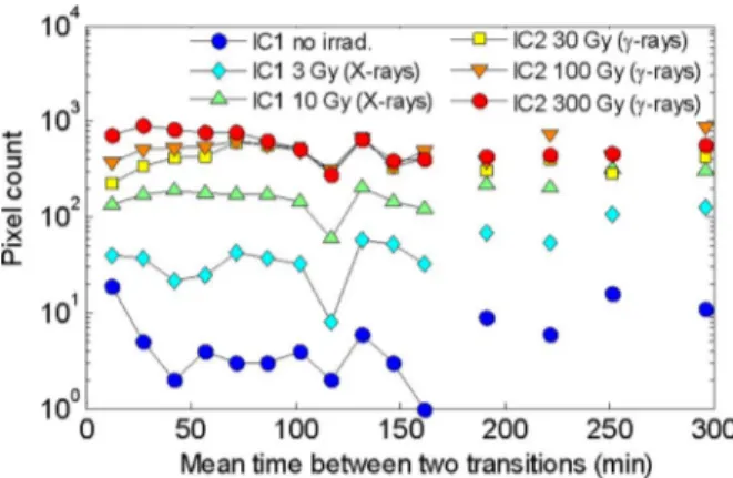
D. Mean Time Between DC-RTS Transition
One of the most important parameter in the characterization of DC-RTS is the mean time between each transition. Indeed, this parameter brings information about the switching time be-tween two configurations of a DC-RTS meta-stable center.
A first approach to study this parameter is to focus on mean time between two transitions to differentiate between TID and DDD induced DC-RTS. As discuss in [12], such methods do not give access to the time constants corresponding to each config-uration change. However, it yields a good overview of the tem-poral characteristics of each pixel DC-RTS signal without the need of processing and analyzing the huge amount of data cor-responding to each transition in each DC-RTS signal.
The mean time between two transitions is deduced from the total observation time divided by the total number of transi-tions. It should be emphasized that if two (or more) different DC-RTS centers are located in the same pixel depletion region, this method will provide a time constant corresponding to the fastest meta-stable center. In the case of one single multi-level DC-RTS center in the pixel, this method will give the time con-stant averaged on all the meta-stable states.
Fig. 13 displays the mean time between two transitions for DDD induced DC-RTS. Proton and neutron exposures roughly present the same exponential trend on the semi-log graph showing that most of the DC-RTS exhibit a short mean inter-transition time. As regards TID induced DC-RTS, the results are shown in Fig. 14. The histogram stays at a constant value for the entire mean time range indicating that, in con-trary to DDD induced DC-RT, TID induced DC-RTS exhibit inter-transition time constant distributed uniformly over the whole temporal detection window. Points above 40 min for Fig. 13 and above 150 min for Fig. 14 are not considered
Fig. 13. Mean time between two DC-RTS transition after several DDD expo-sure. Exponential behavior is seen for the lowest mean times.
Fig. 14. Mean time between two DC-RTS transition after several TID expo-sure. The behavior appears constant on the mean time range. TID corresponds to X-rays irradiations under 30 Gy SiO and to -rays irradiations for dose of 30 Gy SiO and above.
because they correspond to only a few transitions per pixel leading to a poor time constant estimation. Following these ob-servation, it appears that the mean time between two transitions could be another tool to differentiate between TID and DDD induced DC-RTS in CIS.
VIRMONTOIS et al.: TOTAL IONIZING DOSE VERSUS DISPLACEMENT DAMAGE DOSE INDUCED DARK CURRENT RANDOM TELEGRAPH SIGNALS 7
Fig. 15. Cross section of photodiode, (IC) standard design and (DV 1) recessed trench oxide design. Photodiode SCR ends below trench oxide (IC) or PMD (DV 1). Active meta-stable centers induced by TID are represented in red crosses.
Fig. 16. Mapping of DC-RTS for both (IC) and (DV 1) designs after 100 Gy SiO -rays exposure. Number of DC-RTS pixel is dramatically decreased for design (DV 1).
IV. DISCUSSIONABOUTDC-RTS ORIGINS A. Design Variation: Impact on TID Induced DC-RTS
Meta-stable interface states located in oxide trench isolation appear to be the main source of TID induced DC-RTS in stan-dard CIS design [6]. To understand and confirm this phenom-enon, we separately studied pixels with standard photodiode design and with a recessed isolation trench oxide design. In the first case, the depleted volume of the photodiode touches the trench isolation oxide whereas in case of recessed isola-tion trench oxide design, the depleted volume touches the oxide on the top of the photodiode (part of the pre-metal dielectric stack). Fig. 15 illustrates the two kinds of design and the blue dashed line corresponds to the SCR limits. Both designs are irradiated with -rays up to 100 Gy SiO of TID. Mapping results are presented in Fig. 16. We observe a decrease of the DC-RTS number when recessed isolation trench oxide design is used. These results confirm that interface states located in the isolation trench oxide are involved in TID induced DC-RTS. Moreover, non-negligible DC-RTS remains on mapping (DV 1). These results demonstrate that TID induced DC-RTS depends on the type and quality of the interface surface between photo-diode SCR and silicon oxide. This conclusion could explain why TID induced DC-RTS was not observed in previous studies [9] where a different form of oxide isolation, namely LOCOS, was used. The other probable explanation is the fact that absolute dark current levels are much lower in nowadays CIS technology than in the technologies used in previous works. The dark cur-rent shot noise associated with the higher dark curcur-rent values reported in previous work could have hidden the TID induced DC-RTS.
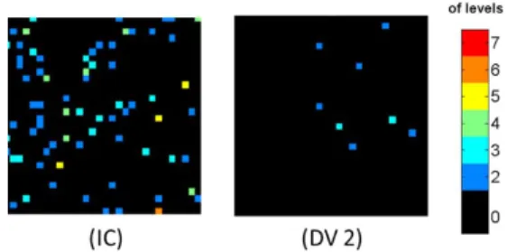
B. Design Variation: Impact on DDD Induced DC-RTS Defects responsible for DDD induced DC-RTS are defined as meta-stable bulk defects located in the depleted volume of the
Fig. 17. Cross section of photodiode, (IC) standard design and (DV 2) standard design with surface reduction. Depleted volume in (IC) is six time higher than the one in (DV 2). Active meta-stable centers induced by DDD are represented in blue circles.
Fig. 18. Mapping of DC-RTS for both (IC) and (DV 2) designs after 39 TeV/g DDD (neutron irradiations). Number of DC-RTS pixel is reduced by a factor six for design (DV 2).
photodiode [2]. The change in depleted volume should modify the number of DC-RTS pixels. Therefore, we decided to use an-other design variation to understand the DDD induced DC-RTS mechanisms. In this design variation, the photodiode architec-ture stayed similar to the one of the standard photodiode but we reduced the photodiode surface by a factor six. Fig. 17 illustrates the two designs. This modification leads to a reduction of the photodiode depleted volume by the same factor (depletion depth remains constant). Results for standard and reduced design are presented in Fig. 18, showing the mapping of DC-RTS pixels after 39 TeV/g DDD (neutron irradiations) for both designs. The number of pixel showing DC-RTS is six times smaller in case of design (DV 2) than in case of design (IC). The number of DDD induced DC-RTS pixels seems to be proportional to the depleted volume. These results confirm the hypothesis of the uniform distribution of meta-stable bulk defects responsible for DDD induced DC-RTS [8], [12].
C. Annealing Behavior of DDD Induced Dark Current and DC-RTS
Identification of defects responsible for dark current increase with DDD remains an open question in solid-state imagers (see for example [17]). Today, it is not well defined which exact electro-active defects or cluster of defects are responsible for dark current increase. However, under the assumption of the universal damage factor [18], whatever the dopant type or con-centration, all devices irradiated at the same DDD present equiv-alent leakage current. As generation rate related to the leakage current is proportional to the concentration of electro-active de-fects [16], the same number of electro-active dede-fects seems to be created at the same DDD. Moreover, as leakage current is independent of the doping type and level, electro-active defects
Fig. 19. Evolution of unannealed fraction of dark current increase and DC-RTS pixels with temperature. Devices studied are exposed to neutron irradiations at several DDD. DC-RTS pixels curve has a different behavior than the dark current curve. These discrepancies show that different types of defects or cluster of defects are related to dark current and to DC-RTS.
tend to probably be intrinsic defects (as opposed to dopant re-lated defects).
Annealing analysis appears to be a useful way to identify point defect types in silicon [19]. Indeed, point defects in sil-icon are known to anneal with temperature and previous studies [19] has determined the annealing temperature of different point defects in silicon. The defects leading to DDD induced DC-RTS belong to the defects leading to DDD induced dark current. To compare these defects, we performed isochronal annealing on the average dark current and on the number of DC-RTS pixels. Fig. 19 presents the temperature annealing behavior of dark current and DC-RTS pixels related to DDD irradiations. For the average dark current, the unannealed factor corresponds to the remaining fraction of current increase that remains after each annealing step. Similarly, the unannealed fraction for DC-RTS corresponds to the fraction of DC-RTS pixels that is still de-tected after each annealing step. As previously explained, for the case of dark current, this factor is proportional to the concentra-tion of electro-active defects related to the dark current. For the case of the number of DC-RTS, the factor is proportional to the concentration of meta-stable defects leading to DDD induced DC-RTS. It is important to note that defects related to DC-RTS are included in the concentration of defects related to the dark current increase after irradiation.
A similar annealing is observed for the three curves related to dark current increase. Their behavior over the annealing tem-perature analysis does not correspond to point defects annealing behavior [19]. Indeed, [19, Fig. 4] illustrates the annealing be-havior of point defects and a steep decrease of the defect frac-tion is observed at each annealing temperature. In Fig. 19, the curve decrease is spread from 20 C to 300 C. This partic-ular behavior could be attributed to cluster annealing kinetic [20]. In this latter hypothesis, defects located around the cluster are annealed first, then the defects at the middle, leading to a spreading of the apparent annealing temperature. Another hy-pothesis could be an annealing combination of different types of defects with close annealing temperatures. The point defects de-fined in [19], corresponding to the annealing temperature close
charges state of the divacancy. Isochronal annealing has been re-ported in [21]. This study present and annealing around 280 C ([21, Fig. 12]). Fleming et al. studies [22], [23] present isochronal annealing of defect concentration obtained with deep level transient spectroscopy. Devices studied in this work are pnp or npn transistors irradiated with neutrons. The most interesting result for this discussion is that the annealing of the peak, namely “deep peak” ([23, Fig. 1]), is close to the an-nealing temperature range of our dark current results. This deep peak contains divacancy, ( ), damage cascade divacancy, (cluster of divacancy) and some vacancy-phosphorus com-plexes (V-P). This work is in agreement with the possible role of cluster in DDD induced dark current increase.
Defects related to DDD induced DC-RTS are part of the de-fects related to dark current increase. However, as we can see in Fig. 19, the number of DC-RTS pixels does not follow the an-nealing behavior of the dark current increase. Indeed, the unan-nealing fraction of DC-RTS pixels remains stable until 100 C and sharply decreases between 120 C and 160 C. This de-crease during isochronal annealing is close to the one observed in CCD [11] and corresponds to a more specific type of defects than the ones of the dark current. That is to say, over the amount of different types of defects leading to dark current increase, only a specific type appears to be responsible for DDD induced DC-RTS.
Previous studies [7], [11] suggested that the P-V center could be responsible for DC-RTS. In [7], the configuration changes of P-V center explained in [24] is associated to a change in the generation rate of the defect leading to a two-level DC-RTS [7]. Moreover, the P-V center annealing temperature (127 C) is around the annealing temperature of the DC-RTS defects ob-served in Fig. 19. Therefore, this center could be a serious can-didate to explain DC-RTS. However, in our device we observe more than two-level DC-RTS which implies more than two con-figurations of the center. To be identified as the center respon-sible for multi-level DC-RTS, the different P-V center configu-rations should induce several different generation rates.
Another explanation could be the intercenter charge transfer [15] between the different charge states of the divacancy inside a cluster. The exchange
was proposed in [9]. But this hypothesis implies a change in the activation energy of the dark current. Therefore, it is not agree with the activation energy close to silicon mid-gap previously reported in the paper.
To conclude about the origin of DDD induced DC-RTS, it is possible that a point defect or cluster of defects are responsible for the phenomenon in silicon, as deduced from the annealing analysis. The bistability of the “deep peak” in [23] related to di-vacancy complexes or didi-vacancy cluster [20] should be investi-gated in the near future.
VIRMONTOIS et al.: TOTAL IONIZING DOSE VERSUS DISPLACEMENT DAMAGE DOSE INDUCED DARK CURRENT RANDOM TELEGRAPH SIGNALS 9
D. Extrapolation to Other Devices
Results presented along this paper provide evidence that DC-RTS in CIS is technologically-dependent and design-de-pendent. Several approaches could then be investigated to treat and to reduce both TID and DDD induced DC-RTS.
Meta-stable defects uniformly distributed in the photodiode SCR seem to be responsible for DDD induced DC-RTS. Re-ducing Photodiode SCR should be an interesting way to reduce this phenomenon. However, such design could only be sug-gested for specific applications because it will also impact and degrade other parameters as quantum efficiency. The distribu-tion of DC-RTS maximum amplitude provides an average expo-nential parameter for several DDD. Under the assumption of the universal damage factor in silicon [18] and the assumption that intrinsic defects are responsible for DDD induced DC-RTS, bulk defects created in silicon during DDD exposure should be universal and the average maximum amplitude should be con-stant for any silicon-based solid state image sensor (without high electric field region) exposed to DDD. This statement could be applied to CIS or CCD unless EFE is an issue in the studied device.
Concerning TID induced DC-RTS design rules could be ap-plied to reduce the phenomenon without impacting significantly sensor performance. Indeed, reducing the surface in contact be-tween isolation trench oxide and the depleted volume of the pho-todiode has been shown to reduce the number of TID induced DC-RTS centers.
Today, 4T pixel CMOS imagers with pinned photodiode [25] are more and more used for scientific applications [26], [27]. The photodiode of such device consist of a potential well formed by P /N/P implantations. The potential well charge is readout thanks to an additional transfer gate and the other readout transistors are identical than in 3T CMOS technology. The advantage, as regards TID induced DC-RTS, is that the depleted volume of the photodiode is isolated from the isolation oxide trench which will dramatically decrease this DC-RTS. DC-RTS results in such devices are currently under study and will be presented in future work.
V. CONCLUSION
Radiation induced two types of Dark Current Random Tele-graph Signal in the photodiode depletion region. One is induced by DDD and the other one by TID. The phenomena arise re-spectively from meta-stable bulk defects and from meta-stable interface states. Generic SRH generation mechanism appeared to be involved in both cases even for the highest DC-RTS am-plitudes. The DC-RTS maximum amplitude histogram and the mean time between transitions seem to be efficient tools to dif-ferentiate between the two DC-RTS. Design variation is used to confirm DC-RTS origins and to provide hardened ways to re-duce DC-RTS in generic CMOS image sensor.
ACKNOWLEDGMENT
The authors would like to dedicate this work to the memory of Dr. Gordon Robert Hopkinson whose work and kindness have given the willingness to study Random Telegraph Signal.
The authors would like to thanks CIMI group for their help, especially F. Corbière and P. Martin-Gonthier for the sensor
conception, P. Cervantes for her help in measurements, and S. Rolando for the critical point of view about the study. They also thank TRIUMF’s committee for providing the proton beam time, S. Quenard, Y. Leo, CEA, Valduc, G. Berger, UCL, Belgium, for their assistance during neutron irradiation and M. Gaillardin, CEA, DAM, for X-ray and -ray irradiations and technical help.
REFERENCES
[1] G. R. Hopkinson, “Radiation effects in a CMOS active pixel sensor,”
IEEE Trans. Nucl. Sci., vol. 47, no. 6, pp. 2480–2484, Dec. 2000.
[2] I. H. Hopkins and G. R. Hopkinson, “Random telegraph signals from proton-irradiated CCDs,” IEEE Trans. Nucl. Sci., vol. 40, no. 6, pp. 1567–1574, Dec. 1993.
[3] M. J. Kirton and M. J. Uren, “Noise in solid-state microstructures: A new perspective on individual defect, interface states and low-fre-quency (1/f) noise,” Adv. Phys., vol. 38, no. 4, pp. 367–468, 1989. [4] C. Leyris, F. Martinez, M. Valenza, A. Hoffmann, J. Vildeuil, and F.
Roy, “Impact of random telegraph signal in CMOS image sensors for low-light levels,” in Proc. ESSCIRC, 2006, pp. 376–379.
[5] J. Janesick, J. T. Andrews, and T. Elliott, “Fundamental performance differences between CMOS and CCD imagers; Part I,” in Proc. SPIE, 2006, vol. 6276, pp. M1–M19.
[6] V. Goiffon, P. Magnan, P. Martin-Gonthier, C. Virmontois, and M. Gaillardin, “Evidence of a novel source of random telegraph signal in CMOS image sensors,” IEEE Electr. Dev. Lett., vol. 32, no. 6, pp. 773–775, Jun. 2011.
[7] I. H. Hopkins and G. R. Hopkinson, “Further measurements of random telegraph signals in proton irradiated CCDs,” IEEE Trans. Nucl. Sci., vol. 42, no. 6, pp. 2074–2081, Dec. 1995.
[8] G. R. Hopkinson, V. Goiffon, and A. Mohammadzadeh, “Random tele-graph signals in proton irradiated CCDs and APS,” IEEE Trans. Nucl.
Sci., vol. 55, no. 4, pp. 2197–2204, Aug. 2008.
[9] J. Bogaerts, B. Dierickx, and R. Mertens, “Random telegraph signals in a radiation-hardened CMOS active pixel sensor,” IEEE Trans. Nucl.
Sci., vol. 49, no. 1, pp. 249–257, Feb. 2002.
[10] T. Nuns, G. Quadri, J.-P. David, O. Gilard, and N. Boudou, “Measure-ments of random telegraph signal in CCDs irradiated with protons and neutrons,” IEEE Trans. Nucl. Sci., vol. 53, no. 4, pp. 1764–1771, Aug. 2006.
[11] T. Nuns, G. Quadri, J.-P. David, and O. Gilard, “Annealing of proton-induced random telegraph signal in CCDs,” IEEE Trans. Nucl. Sci., vol. 54, no. 4, pp. 1120–1128, Aug. 2007.
[12] V. Goiffon, P. Magnan, O. Saint-Pé, F. Bernard, and G. Rolland, “Multi level RTS in proton irradiated CMOS image sensors manufactured in a deep submicron technology,” IEEE Trans. Nucl. Sci., vol. 56, no. 4, pp. 2132–2141, Aug. 2009.
[13] A. M. Chugg, R. Jones, M. J. Moutrie, J. R. Armstrong, D. B. S. King, and N. Moreau, “Single particle dark current spikes induced in CCDs by high energy neutrons,” IEEE Trans. Nucl. Sci., vol. 50, no. 6, pp. 2011–2017, Dec. 2003.
[14] G. Vincent, A. Chantre, and D. Bois, “Electric field effect on the thermal emission of traps in semiconductor junctions,” J. Appl. Phys., vol. 50, no. 8, pp. 5484–5487, Aug. 1979.
[15] S. Watts, J. Matheson, I. Hopkins-Bond, A. Holmes-Siedle, A. Moham-madzadeh, and R. Pace, “A new model for generation-recombination in silicon depletion regions after neutron irradiation,” IEEE Trans. Nucl.
Sci., vol. 43, no. 6, pp. 2587–2594, Dec. 1996.
[16] W. Shockley and W. T. Read, “Statistics of the recombinations of holes and electrons,” Phys. Rev., vol. 87, no. 5, pp. 835–842, Sep. 1952. [17] C. Virmontois, V. Goiffon, P. Magnan, S. Girard, C. Inguimbert, S.
Petit, G. Rolland, and O. Saint-Pe, “Displacement damage effects due to neutron and proton irradiations on CMOS image sensors manufac-tured in deep sub-micron technology,” IEEE Trans. Nucl. Sci., vol. 57, no. 6, pp. 3101–3108, Dec. 2010.
[18] J. R. Srour and D. H. Lo, “Universal damage factor for radiation-in-duced dark current in silicon devices,” IEEE Trans. Nucl. Sci., vol. 47, no. 6, pp. 2451–2459, Dec. 2000.
[19] G. D. Watkins, “Intrinsic defects in silicon,” Mater. Sci. Semiconduct.
Process., vol. 3, pp. 227–235, 2000.
[20] J. W. Palko and J. R. Srour, “Amorphous inclusions in irradiated silicon and their effects on material and device properties,” IEEE Trans. Nucl.
paramagnetic resonance and electron-nuclear double resonance of the Si-E center,” Phys. Rev., vol. 134, no. 5A, pp. 1359–1377, 1964.