HAL Id: hal-02270894
https://hal.archives-ouvertes.fr/hal-02270894
Submitted on 26 Aug 2019
HAL is a multi-disciplinary open access
archive for the deposit and dissemination of
sci-entific research documents, whether they are
pub-lished or not. The documents may come from
teaching and research institutions in France or
abroad, or from public or private research centers.
L’archive ouverte pluridisciplinaire HAL, est
destinée au dépôt et à la diffusion de documents
scientifiques de niveau recherche, publiés ou non,
émanant des établissements d’enseignement et de
recherche français ou étrangers, des laboratoires
publics ou privés.
O-band DAC-less PAM-4 generation with a silicon
dual-drive Mach-Zehnder Modulator
Lucas Deniel, Mathilde Gay, Diego Perez-Galacho, Charles Baudot, Laurent
Bramerie, Oskars Ozolins, Frédéric Boeuf, Laurent Viven, Christophe
Peucheret, Delphine Marris-Morini
To cite this version:
Lucas Deniel, Mathilde Gay, Diego Perez-Galacho, Charles Baudot, Laurent Bramerie, et al..
O-band DAC-less PAM-4 generation with a silicon dual-drive Mach-Zehnder Modulator. 21st European
Conference on Integrated Optics (ECIO 2019), Apr 2019, Gand, Belgium. ecio-conference.org, Poster
session (T.Po2), 2019, 2019 Proceedings. �hal-02270894�
O-band DAC-less PAM-4 generation with a silicon dual-drive
Mach-Zehnder Modulator
(Student Paper)
Lucas Deniel1, Mathilde Gay2, Diego Pérez-Galacho1,3, Charles Baudot4, Laurent Bramerie2, Oskars Ozolins5, Fréderic Boeuf4, Laurent Viven1, Christophe Peucheret2, Delphine Marris-Morini1
1 Centre de Nanosciences et de Nanotechnologies, CNRS, Univ. Paris-Sud, Université Paris-Saclay, 91120 Palaiseau, France
2 Univ Rennes, CNRS, FOTON – UMR 6082, F-22305 Lannion, France
3 now at : ITEAM research institute, Universitat Politècnica de València, Camino de Vera s/n, 46022, Valencia, Spain
4 ST Microelectronics, 850 rue Jean Monnet, 38920 Crolles, France 5 Networking and transmission Laboratory, RISE AB, Kista, Sweden
e-mail: [email protected]
ABSTRACT
4-level pulse amplitude modulation (PAM-4) is the chosen modulation format for next generation optical short-reach data communications such as intra-datacenter communications. On-chip generation of PAM-4 signals is possible using a single dual-drive Mach-Zehnder modulator (MZM). By driving the modulator with two voltage-unbalanced binary signals it is possible to avoid any power hungry electrical digital-to-analog converter (DAC). PAM-4 signal generation at 20 Gbit/s is demonstrated using a silicon dual-drive MZM in the O-band. A bit error rate (BER) of 3.810-3 is measured at -6 dBm input power.
Keywords: Silicon, Mach-Zehnder modulator, PAM-4, O-band, DAC-less. 1. INTRODUCTION
For the next generation of intra-datacenter and short-reach data communications, 4-level pulse amplitude modulation (PAM-4) has been chosen as a convenient format to fulfill the increasing spectral efficiency requirements. Silicon photonics is a promising technology for these applications as it provides economical, flexible, and low-power solutions, in addition to its mature complementary metal-oxide semiconductor (CMOS) fabrication process and the possibility of co-integration with electronics [1, 2].
Usually, PAM-4 signal generation is done in the electrical domain, and this signal is used to drive the electro-optical modulator. In this case, power hungry digital-to-analog converters (DAC) are needed to convert 2-level non-return-to-zero (NRZ) data-streams into 4-level ones. For this reason, the generation of PAM-4 signals in the optical domain was proposed and successfully demonstrated using various structures of silicon modulators on which two different NRZ binary sequences were directly applied. These structures are sometimes referred to as optical DACs, and most of these demonstrations were done in the C-band [3-5]. Interestingly, the well-known dual-drive Mach-Zehnder modulator (MZM) structure is used for classical OOK modulation, but it was demonstrated that it could also be used for quadrature phase shift keying (QPSK) and PAM-4 generation, making it an interesting choice for the evolving transmission standards. [6, 7]
We demonstrate optical PAM-4 generation at 20 Gbit/s using an O-band silicon dual-drive MZM. In the first part, we introduce the MZM design and the phase shifter characteristics. A numerical model is then used to find out the peak-to-peak voltages to apply on the MZM arms to obtain 4 equally spaced intensity levels while benefiting from the transmission full dynamic range. Experimental results are then reported, including bit error rate measurements.
2. MODULATOR DESIGN AND PHASE SHIFTER CHARACTERISTICS
The device fabrication was carried out by ST-Microelectronics on a 300-mm silicon-on-insulator (SOI) technological platform [8]. The optical access of the chip are ensured by grating couplers. The combiner and splitter of the MZM structure are 3-dB 12 multimode interference (MMI) based couplers. Each arm contains a phase shifter which consists in a 1-mm-long lateral PN junction embedded in a rib waveguide, operating in depletion regime. The waveguide height is 300 nm and its width is 400 nm, allowing propagation of the fundamental TE mode, while the slab part is 50-nm thick. The targeted doping concentrations are 51017 cm-3 for the P region and 4.51017 cm-3 for the N region. Higher doping concentrations of about 1019 cm-3 are used near the electrical contacts to reduce the access resistance, thus enhancing the modulator bandwidth. Traveling wave coplanar electrodes on the surface of the chip are used for radio-frequency (RF) waves propagation and metallic
strips are used as resistors (heaters) close to each arm to thermally tune the static operating point of the MZM, by applying a DC voltage.
Static characterizations of the phase shifter efficiency were made experimentally by tracking the resonance wavelengths of a ring resonator, as it allows a precise measurement of the phase variation within the waveguide as a function of the applied voltage. The measured phase shifter efficiency varies from 1.1 V cm at -0.5 V to 1.4 V cm at -7 V. A 17-GHz electro-optical bandwidth was measured on the MZM using an Agilent 86030A 50 GHz Lightwave Component Analyzer.
The phase shifter insertion loss was estimated as a function of the voltage through a numerical model. First, carrier concentrations within the PN junction as a function of the applied voltage are obtained using an electrical simulation. Soref model is then used to calculate the corresponding local absorption coefficients, and a mode solver is finally used to estimate the total effective attenuation factor of the waveguide. Loss estimation varies from 1.8 dB mm-1 at 0V to 1.1 dB mm-1 at -7V.
3. PAM-4 MZM MODEL AND COMPARISON WITH EXPERIMENTAL RESULTS
As the effective index change is not linear with the applied voltage, and as the insertion loss depends on the applied voltage, finding the dynamic voltage amplitudes to apply on each arm to obtain 4 equally-spaced intensity levels while maximizing the extinction ratio in the optical domain is not straightforward. For this reason, the following equations are numerically implemented to model the MZM:
(
)
(
)
(
)
IN 2
exp ( ) exp j ( )
2
n eff eff n eff eff n
E E V L n n V L = − + + (1) 2 2 1 2 OUT 2 H H j j E e E e E − + = (2) where EIN is the input electric field, En is the electric field at the output of arm labelled n, EOUT is the output electric field, L is the phase shifter length, is the wavelength, H is the static phase shift introduced by thermal heaters,
eff and neff are the effective attenuation factor and refractive index of the optical mode, respectively, eff(Vn) and neff(Vn) are the effective attenuation factor change and refractive index change of the optical mode, respectively, under the application of the voltage Vn on the phase shifter labelled n. eff +eff(Vn) is estimated and neff(Vn) is calculated as described in the previous section.
Fig. 1(a) shows the PAM-4 levels obtained with the MZM numerical model by applying peak-to-peak voltages of 4 V on one arm of the MZM and 7 V on the other. Fig. 1(b) shows an eye diagram obtained experimentally by applying the same voltages to the real silicon MZM, biased at the quadrature point. The matching of level spacings between the two figures demonstrates the numerical model accuracy.
Figure 1. (a) Obtained PAM-4 levels by applying a 4-V peak-to-peak voltage on one arm and 7-V peak-to-peak voltage on the second arm on the silicon MZM numerical model. (b) Experimental eye diagram obtained after applying the same peak-to-peak voltages on the silicon
MZM.
4. BER MEASUREMENTS
A BER measurement is conducted to evaluate the MZM PAM-4 performance under this dual-driving method. For this experiment, light is produced by an external cavity laser at 1310 nm and input to the device after being amplified with a semiconductor optical amplifier (SOA). At the output of the chip, the modulated beam is amplified with a praseodymium doped fiber O-band amplifier and split in two paths with a fibered directional coupler. One half of the power is sent to a 25-GHz oscilloscope displaying the eye-diagram in real time. The other half is sent to a 40-GHz photodiode and the converted electrical signal goes through a 35-GHz amplifier before being received
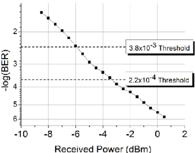
by the error counter of a BER tester. Two complementary pseudo random binary sequences (PRBSs) are generated electrically at a 10-Gbit/s rate. One of them is delayed by 200 ps with an RF tunable delay line, and both signals are amplified with tunable gain RF amplifiers. A -4-V DC voltage is added on both lines with DC bias tees to bias the PN junction in reverse. The two driving signals are then injected into the RF electrodes of the MZM via RF probes before being absorbed by 50 terminations loaded after DC blocks on the electrical output. The peak-to-peak voltages are set to 4 V on one arm and 7 V on the other one by tuning the RF amplifier gains. The optical power received on the photodiode is swept from -8.5 to 0.5 dBm for the BER measurement. Fig. 2 shows the obtained BER values as a function of the received power.
Figure 2. Measured O-band PAM-4 BER with the silicon MZM driven by a 7-VPP and a 4-VPP PRBS as a function of the received optical power.
It can be seen that the BER is under the 3.810-3 hard-decision forward-error-correction (HD-FEC) threshold for a received power of -6 dBm and under the 2.210-4 KP4 threshold for a received power of -3.4dBm.
5. CONCLUSIONS
A 20-Gbit/s PAM-4 signal was generated at 1310 nm using a silicon dual drive MZM driven by two different NRZ binary signals. After an introduction of this modulator design and characteristics, a numerical model was presented and used to find out the optimum voltages to apply to each arm of the MZM for PAM-4 generation. Finally, a BER under the HD-FEC threshold of 3.810-3 was measured for a received power of -6 dBm using the silicon MZM as an optical PAM-4 generator.
ACKNOWLEDGEMENTS
This work was supported by the European project Cosmicc (H2020-ICT-27-2015-688516).
REFERENCES
[1] IEEE P802.3bs 400 GbE Task Force, http://www.ieee802.org/3/bs/index.html.
[2] W. Shi et al.: Silicon photonic modulators for PAM transmissions, J. Opt., vol. 20. 083002, July 2018. [3] A. Roshan-Zamir et al.: A 40Gb/s PAM4 optical DAC silicon microring resonator modulator transmitter, in
Proc. MWSCAS 2017, Boston, MA, 2017, pp. 1089-1092.
[4] D. Patel et al.: Silicon photonic segmented modulator-based electro-optic DAC for 100Gb/s PAM-4 Generation, IEEE Photon. Technol. Lett., vol. 27. pp. 2433-2436, Dec. 2015.
[5] R. Li et al.: Silicon photonic ring-assisted MZI for 50Gb/s DAC-less and DSP-free PAM-4 transmission,
IEEE Photon. Technol. Lett., vol. 29. pp. 1046-1049, June 2017.
[6] L. Zheng et al.: Silicon PAM-4 optical modulator driven by two binary electrical signals with different peak-to-peak voltages, Opt. Lett., vol. 42. pp. 2213-2216, June 2017.
[7] D. Pérez-Galacho et al.: QPSK modulation in the O-band using a single dual-drive Mach-Zehnder silicon modulator, J. Lightw. Technol., vol. 36. pp. 3935-3940, Sept. 2018.
[8] C. Baudot et al.: Daphne silicon photonics technological platform for research and development on WDM applications, in Proc. SPIE 9891, 2016, 98911D.