M. Benhaliliba
Material TechnologyDepartment, Physics Faculty, USTOMB University, BP1505 Oran, Algeria
Received: 09 February 2016 / Accepted: 27 December 2016 / Published online: 01 January 2017
ABSTRACT
The photovoltaic properties of a good rectifying Al/ZnO/pSi/Al Schottky diode are studied. The diode was fabricated from two processes like ultrasonic spray pyrolysis @ 350°C for the ZnO layer on p-type Si substrate and thermal evaporation in vacuum at 10-6Torr for the metallic contacts. The current-voltage (I-V) measurements show a good rectifying behavior. Therefore, the extracted parameters are calculated in dark and illumination in one hand and under heating conditions in other hand. Ideality factor is lower around 1.5. Barrier height and series resistance, determined by Cheung-Cheung and Norde methods, are found to be 0.6-0.9 V and 1.4-5.4 kΩ. The parameters are influenced by increasing temperature; barrier height goes from 0.7 to 0.9 V and series resistance range within the range 1.2 -2.5 kΩ. Under light (150 W), the open circuit voltage and short circuit are found to be 0.09 V and 0.3 µA, the fill factor is of 0.44.
Keywords: Schottky barrier diode; the sprayed ZnO film; Current-voltage characteristics; Good rectifying behavior; Open circuit voltage; Barrier height; Series resistance.
Author Correspondence, e-mail:mbenhaliliba@mail.com
doi:http://dx.doi.org/10.4314/jfas.v9i1.35
Journal of Fundamental and Applied Sciences is licensed under aCreative Commons Attribution-NonCommercial 4.0 International License.Libraries Resource Directory. We are listed underResearch Associationscategory.
1. INTRODUCTION
Through the last decades, ZnO thin films and devices have been extensively investigated due to their potential applications in optoelectronic devices and photovoltaic cells.ZnO has attracted researchers in films and devices [1-2], it has intensively grown onto different substrates,like p-type silicon, InP, graphite, as thin films, Schottkybarrier diodes (SBD) and heterostructures (HS) [3-5].The ZnO devices based on ZnO have been fabricated by various methods like sputtering [6], spin coating and spray pyrolysis [7-8].The application of ZnO device are various, like gas sensors and solar cells [9-10].In the aim to prepare a photovoltaic device, we fabricate a Schottky diode based on a wide band gap semiconductor ZnO,Eg> 3 eV with a good rectifying behavior. The study’s aim is to replace standard Schootky diode by those based on wide band gap oxide semiconductor.
2. PREPARATION OF THE THIN FILM AND FABRICATION OF DIODE
ZnO films are grown by USPD route from zinc acetate (Zn (CH3COO)2, 2H2O) used asprecursor. 0.1 mole of zinc acetate was dissolved in 100 ml of methanol. Both Al and Sn doping were added from the aluminum chloride (AlCl3) and tin chloride (SnCl2) to the precursor with a concentration of 2%. The used substrates were successively cleaned by methanol for 15min and distilled water for 20 min. We deposit our films at fixed substrate temperature of 350 °C and the time deposition was 5min and the distance nozzle substrate was around 5cm. The metallic contacts were made by thermal evaporation in vacuum at 10-6Torr, using a mask.The cross section of Al/ZnO/pSi/Al structure is sketched in figure1. The obtained Al contacts are circular with a diameter of 1.5 mm and thickness of 250 nm.Measurements of current-voltage dark and illumination were carried out by Keithley source meter unit SMU 2400 as shown in figure 1.
Fig.1. A schematic cross-section of the Al/ZnO/pSi/Al structure
3. RESULTS AND DISCUSSION
3.1. The schottky diode investigation under dark
The figure 2 shows the current-voltage measurements in dark conditions of A/ZnO/pSi Schottky diode. The I-V characteristics in dark exhibit a good rectifying profile of 3900 at ±2V. The exponential profile of the forward current-voltage characteristics depends strongly on the property of active material used fordiode. The I-Vcharacteristics exhibit a slope which depends on two magnitudes the ideality factor (n) and the reverse saturation current. From the I-V semilog plot, under condition of V >3kT/q in the forward direction [11], the ideality factor is determined as follows [12];
)
ln(I
d
dV
kT
q
n
(1)Where q=1.6 10-19 C is the carrier charge, T=300 K is the absolute temperature, k=8.625 10-5 eV/Kis the Boltzmann constant, dlnI /dV is the slope of straight part of the forward I-Vcurve. The parameter n gives detail information about the recombination process to be taken place in the diode and shape of the interfaces. The ideality factor values were calculated from the slope and intercept of figure 3. Under dark condition, n is of 3.5 (greater than unity).The obtained values of n ranged within the gap 2.49-3.02 in dark under heating condition as tabulated below (table 1). As found in literature, ideality factor depending on temperature is ranged within1.7-3.5 [13]. Another parameter that affects the exponential part of I-V
characteristics is the saturation current I0 which gives the numbers of charges capable to overcome the energetic barrier in reverse bias voltage. According to the thermo-ionic emission mechanism, the current versus voltage depending on I0is expressed as follows [6],
) ) ( exp( 0 nkT IR V q I I s (2)
Fig.2. The semilog plot of the current-voltage characteristics of Al/ZnO/pSiSchottkydiode measured at several light powers.
V is the applied voltage, Rsis series resistance and I0is given by [11],
) exp( ² * 0 kT q T AA I B (3)
Where A is the diode contact area (0.0176cm2), A* is the Richardson constant of p-Si equal to 32 A cm-²K-², T is temperature of ambient fixed at 300 K and ΦB is the zero-bias barrier height. The saturation currents were obtained from the linear portion intercept of logI at V = 0. The measurement of the current-voltage variation under temperature is shown in figure 4. However, the height barrier is expressed as follows [14];
) ² * ln( 0 I T AA q kT B (4)
Fig.3. Plotting of I-V characteristics dark-illumination of Al/ZnO/pSiSchottkydiode (up). Geometrical construction of the maximum power point, open circuit voltage and short circuit
current at 150 Ware displayed (down).
As indicated in previous reports, the height barrier and resistance are close to those obtained in this work. The series resistance, Rs=ΔV/ΔI, is accurately determined from the slope of the linear part of the I-V characteristics for the high voltage > 1V. The found values, indicated in table 1, a couple of kilo-ohms are a bit higher, which explain the interface occurrence in our devices. A power-law dependence on the applied voltage is expressed as I α Vm , the logI-logV plot gives three regions assigned to different conduction mechanisms (not shown
here). Our SBD presents a barrier height of 0.7-0.9 V and Rs of 1.5-5.5 kΩ, these obtained values are in good agreement with those found in literature, a barrier height of 0.76 V and series resistance of 6.7kΩ [6]. A deviation in the ideality factor is observed caused by the interface state density and series resistance for the strong currents. It is evaluated that at higher voltages, the series resistance becomes a significant proportion of the applied voltage. The series resistances are estimated by different methods like Cheung and Cheung model [15].The power law behavior I α Vm, is generally revealed by a double logarithmic forward bias current-voltage plot. The forward bias log plots of the I-V characteristics for the Al/ZnO/pSi diode are displayed, in which three separate linear regions, indicating different conduction mechanisms, are defined. The slopes are calculated from the logI-logV plots and are found to be 1.3, 3.1 and 4.3 respectively for the region I, II and III (not shown here). At low voltage (region I) m<2, it seems to ohmic conduction mechanism while in the region II (0.15<V<0.7 V), it exhibits a slope greater than 2, the as- fabricated device presents a space charge limited current mechanism, well known by SCLC acronym, dominated by a presence of traps in the ZnO layer band gap. The slope of the region III is higher (m> 4), SCLC still dominates here. As shown in figure 3, the regions are result of two different mechanisms of charge carrier transport through the junction metal semiconductor, then the series resistance and barrier height which are the origin of above mentioned mechanisms are given by the function of Norde F(V) under the V>3kT/q condition [16];
) ² * ) ( ln( ) ( T AA V I q kT V V F (5)
The barrier height is then given by,
q kT V V F B 0 0) ( (6)
Using to the obtained values of V0=0.32 V, F(V0)=0.42 V from the figure 6, the barrier height is then of 0.47 V. Besides, the series resistance is then deduced from the following relation,
This function is available when the mechanism tends exhaustively to thermionic one. In contrast, when the resistance effect dominates, the two parameters ΦBand Rs are determined from the function H(I);
) ² * ln( ) ( ) ( T AA I q nkT V I H (8)
Fig.4. Plotting of I vs. V (semilog scale) measured at various temperatures (295K-380K) of Al/ZnO/pSi Schottky diode .
However, the function H(I) depending on ΦB and Rs,as shown in fig.5, can be expressed as follows, I R n I H( ) B s (9)
resistance deduced from the plot of H(I) are evaluated at 0.69 V and 200 Ω.When the effect of resistance is important, then the equation 1 will be modified according to Cheung’s function at higher voltage as follows; in the gap of higher voltage, the applied method developed by Cheung and Cheung is required,
500.0µ 1.0m 1.5m 0.0 0.1 0.2 0.3 0.4 0.5 Current (A) d V /d ln I (V ) 4 5 6 H (I) ( V )
Fig.5. Sketch of dV/dlnI (left) and H(right) vs. current of Al/ZnO/pSi/Al Schottky diode fabricated by spray pyrolysis process.
) ( ln q kT n I R I d dV s (10)
The obtained parameters such as height barrier, series resistance, extracted by both Cheung-Cheung and Norde methods, are close.
3.2. The current-voltage characteristics of Al/ZnO/pSi/Al Schottly diode under illumination.
When diodes are illuminated, the obtained values of I ranged from 1.1 to 42 nA are gathered in table 1. As observed in figure 3, the photo-response Iph /Idarkis found to be 1730-3891 as listed in table1. The potential Vmis deduced approximately from the following relation [17];
) 1 ln( kT qV q kT V V OC oc m (11)
Fig.6. A sketch of Norde function versus bias voltageof Al/ZnO/pSi/Al Schottky diode fabricated by spray pyrolysis process, V0and F(V0) are displayed by a red arrow.
Deduced from the geometrical construction, as displayed in the inset of fig.3, Vm and Imare approximately of 0.051V and 0.14µA, and the maximum power is found to be 7 nW. According to eqn. 12, an approximate fill factor is assessed at 0.44, 150 watt corresponds to 100mW/cm2(1.5 AM). Similar trends were found in previous works [17].
3.3. The dark current-voltage characteristics of Al/ZnO/pSi/Al Schottky diode at various temperatures.
The temperature dependence of I-V characteristics under dark is plotted in figure 4 within the 295-380 K temperature range. It is observed from the sketch a non-ideal behavior of the diode, so exhibits a rectifying profile. Therefore, the ideality factor is greater than unity as listed in table 1; it goes from 1.1 to 3.5. The ideality factor decreases with increasing temperature as indicated in table1. The parameter n depending on temperature is ranged within 1.7-3.5 as reported in the literature [13]. As can be easily seen from the figure 4, a clear deviation from the linearity in the forward current region is detected. This deviation is due to the series
resistance.The obtained values of I0 ranged from 14 to 450 nA as a result of temperature are listed in table 1.It is revealed that ideality factor less or equal to 2 explains both the electron-hole recombination and diffusion processes whereas n greater than 2 only the domination of recombination process occurs. As tabulated below, the obtained values of n demonstrate the existence of a combination of recombination and diffusion currents in the as fabricated diodes. The height barrier is one of the main parameters extracted from I-V characteristics of the Schottky barrier diode. The values of ΦB are gathered in table1; from them we remark that as soon as the temperature arises as soon as ΦB ascends continuously from 0.74 to 0.89 V. This phenomenon is due to a number of free charge carriers which have enough energy to surmount the barriers and contribute to conduction with increasing temperature.
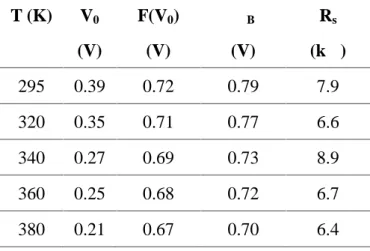
The current (semi log scale) versus temperature for the different voltages in reverse region is depicted in figure 4A. The current against temperature for the various voltages shows a linear variation and it decreases with an increase in voltage. The ZnOSchottky diodes measured at various temperatures. Traditionally, the method used to extract the ideality factor n and the barrier height BHfrom I-V characteristic of a Schottky diode is based on simple thermionic emission theory. However, this approach isnot valid when there exists a series resistance Rsin a real diode. It was found that linear regions for the semi-log I-V plots were slight and it is difficult to precisely extrapolate to zero voltage. Energy-band diagram of Al/ZnO/pSiSchottky diode is depicted in fig.4B. The influence of temperature on the Norde function is revealed as listed in table 2. Both the parameters V0, F(V0) and ΦB decreased when the temperature is increasing while the series resistance is highest (8.9 kΩ) for 340 K.
(kΩ) P mW/cm² 0 3.5 32 0.74 5.4 -40 1.9 42 0.79 2.1 1730 60 1.5 16 0.89 2.8 1945 80 1.1 2 0.86 1.4 3502 100 1.6 1.1 0.90 1.6 3891 T (K) 295 3.02 34 0.74 2.5 320 2.55 73 0.79 2.5 340 2.49 14 0.89 1.6 360 2.51 260 0.86 1.0 380 2.67 450 0.89 1.2 4. CONCLUSION
The Al/ZnO/p-Si/Al Schottky diode was fabricated by a facile technique controlling parameters like film and contacts thickness, vacuum pressure and temperature. Our device exhibits a good rectifying profile and a lower ideality factor <3.6. Height barrier is around 0.7 V. the photocurrent is evaluated at 2 mA, this obtained value leads us to us the as fabricated diode in photodiode application. Effect of light power and temperature on microelectronic parameters was clearly observed. Such device can be used in solar cells, photoconductor and photodiode.
Table 2. Norde parameters, height barrier, series resistance of Al/ZnO/pSi/Al diode at various heating temperatures for forward current range.
T (K) V0 (V) F(V0) (V) ΦB (V) Rs (kΩ) 295 0.39 0.72 0.79 7.9 320 0.35 0.71 0.77 6.6 340 0.27 0.69 0.73 8.9 360 0.25 0.68 0.72 6.7 380 0.21 0.67 0.70 6.4 5. ACKNOWLEDGMENTS
The work is included in the PNR projects under contract number 8/U311/R77 and U311/R81, supported by ‘‘Agencethématique de rechercheen science ettechnologie’’ (ATRST)
http://www.atrst.dz, and National administration of scientific research (NASR)
http://www.nasr.dz. This work is a part of CNEPRU project N° B00L02UN310220130011 supported by Oran University of Sciences and Technology www.mesrs.dz, and
www.univ-usto.dz. The first authors are grateful for the assistance of The Head of DUBTAM-Renewable Energy Research Laboratory and his staff
http://www.dicle.edu.tr/dubtamand the virtual library of SNDLhttps://www.sndl.cerist.dz.
6. REFERENCES
[1] Benhaliliba M, Benouis C.E, Aida M.S, Sanchez Juarez A and Yakuphanoglu F, J. Sol-Gel Sci. Technology (2010) doi 10.1007/s10971-010-2258-x.
[2] Benouis C.E, Benhaliliba M, Sanchez Juarez A, Aida M.S, F. Chami and Yakuphanoglu F. J. Alloys Compd. 490 (2010) 62-67.
[3] Ocak Y. S, Kulakci M, Turan R, Kilicoglu T, Gullu O, J. Alloys Compd.509 (2011) 6631-6634.
[9] Herran J, Fernandez I, Tena Zaera R, Ochoteco E, Cabanero G, Grande H, Sensors and Actuators B 174(2012) 274-278.
[10] Ozgur U, Alivov Y.I, Liu C, Teke A, Reshchikov M.A, Dogan S, Avrutin V, Cho S.J and Morkoç H, J. Appl. Phys.98 (2005) 041301.
[11]Sze S.M, Kwok K. Ng, Physics of Semiconductors Devices Wiley New York, 2007. [12]Karatas S, Yakuphanoglu F, Mater. Chem. Phys. 138 (2013) 72-77.
[13]Young S.J, Chang S.J, Ji L.W, Meen T.H, Hsiao C.H, Liu K.W, Chen K. J and Hu Z.S, Microelec. Eng. 88 (2011) 113-116.
[14] Zhang X, Hai F, Zhang T, Jia C, Sun X, Ding L, Zhang W, Microelec Eng. 93(2012) 5-9.
[15] Cheung S.K, Cheung N.W, Appl. Phys. Lett. 49 (1986) 85. [16] Norde H, J. Appl. Phys.50 (1979) 505218.
[17] Wurfel P, Physics of Solar Cells, 2005 Wiley.
How to cite this article:
Benhaliliba M. The photovoltaic properties of a good rectifying al/n-zno/p-si/al schottky diode used in solar cell. J. Fundam. Appl. Sci., 2017, 9(1), 605-617.