HAL Id: hal-01162066
https://hal.sorbonne-universite.fr/hal-01162066
Submitted on 9 Jun 2015
HAL is a multi-disciplinary open access
archive for the deposit and dissemination of
sci-entific research documents, whether they are
pub-lished or not. The documents may come from
teaching and research institutions in France or
abroad, or from public or private research centers.
L’archive ouverte pluridisciplinaire HAL, est
destinée au dépôt et à la diffusion de documents
scientifiques de niveau recherche, publiés ou non,
émanant des établissements d’enseignement et de
recherche français ou étrangers, des laboratoires
publics ou privés.
Impact of defect tolerance techniques on the criticality
of a SRAM-based Mesh of Cluster FPGA
Adrien Blanchardon, Roselyne Chotin-Avot, Habib Mehrez, Emna Amouri
To cite this version:
Adrien Blanchardon, Roselyne Chotin-Avot, Habib Mehrez, Emna Amouri. Impact of defect tolerance
techniques on the criticality of a SRAM-based Mesh of Cluster FPGA. ReConFig 2014 -
Interna-tional Conference on ReConFigurable Computing and FPGAs, Dec 2014, Cancun, Mexico. pp.1-6,
�10.1109/ReConFig.2014.7032508�. �hal-01162066�
Impact of defect tolerance techniques on the
criticality of a SRAM-based Mesh of Cluster FPGA
Adrien Blanchardon
1,2, Roselyne Chotin-Avot
1,2, Habib Mehrez
1,2, Emna Amouri
1,2 1- Sorbonne Universit´es, UPMC Univ Paris 06, UMR 7606, LIP6, F-75005, Paris, France2- CNRS, UMR 7606, LIP6, F-75005, Paris, France Email: adrien.blanchardon@lip6.fr
c
2014 IEEE. Personal use of this material is permitted. Permission from IEEE must be obtained for all other uses, in any current or future media, including reprinting/republishing this material for advertising or promotional purposes, creating new collective works, for resale or redistribution to servers or lists, or reuse of any copyrighted component of this work in other works. DOI: 10.1109/ReConFig.2014.7032508
Abstract—As device sizes shrink, circuits are increasingly prone to manufacturing defects. One of the future challenges is to find a way to use a maximum of defected manufactured circuits. One possible approach to this growing problem is to add redundancy to propose defect-tolerant architectures. But, hardware redundancy increases area. In this paper, we propose a method to determine the most critical elements in a SRAM-based Mesh of Clusters FPGA and different strategies to locally insert hardware redundancy. Depending on the criticality, using defect tolerance, area and timing metrics, five different strategies are evaluated on the Mesh of Clusters architecture. We show that using these techniques on a Mesh of Clusters architecture permits to tolerate 4 times more defects than classic hardware redundancy techniques applied on industrial mesh FPGA. With local strategies, we obtain a best trade off between the number of defects bypassed (37.95%), the FPGA area overhead (21.84%) and the critical path delay increase (9.65%).
I. INTRODUCTION
The increase of integration density according to Moore’s law is being slowed due to economic and physical limits. As manufacturing yield decreases, one of the future challenges is to find a way to use a maximum of manufactured circuits tolerating physical defects all over the chip [1] [2]. Compared to ASICs, FPGAs have attained a central focus due to their ability to integrate more complex applications, their flexibility and good performance. Considering that FPGAs based on nanotechnology may have a defect rate of 20% [3] [4], propose techniques to avoid these defects is necessary. Several studies examined the effect of redundancy techniques on the performance of FPGAs. These techniques can be classified into software-based and hardware-based techniques. Software-based techniques avoid defective resources using configuration tools [5] [6] [7] [8]. However, their efficiency relies on the ability of the tools to take into account the defects and the number of unused resources. Hardware-based techniques use spared resources in the architecture. Correct a defect is to bypass the defective element by the added one [9] [10] [11]. Hardware-based techniques can be implemented in FPGAs to increase their reliability. The studies in [12] and [13] showed that using hardware redundancy on the top level of the FPGA requires more area to tolerate the same number of defects than a hardware redundancy applied inside local interconnect. As theses techniques increase significantly the FPGA area, it is therefore necessary to apply a local redundancy inside the FPGA depending on the criticality of each block. The focus of
this paper is to present a method to determine the criticality of each block and to apply different local hardware-based tech-niques to prevent defects without much decrease performance. The remainder of the paper is organized as follows. Section II describes the architecture of the FPGA under study. Section III presents different defect-tolerant schemes applied at different levels in the FPGA. Section IV details the proposed method to determine the criticality of each block. Simulation results are presented in section V. Finally, section VI concludes this paper.
II. FPGAARCHITECTURE
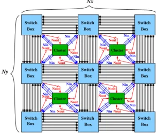
In FPGAs, the interconnect takes up 90% of the total area and is responsible of a large part of the circuit delay [14] [15]. To reduce these costs, we propose in [14] a Mesh of Clusters architecture (Fig.1). With this kind of architecture based on clustering, the total area can be reduced by 42% compared to the VPR Style clustered Mesh.
Nx Ny Nin Nout Nout Nin Nin Nout Nin Nout Nin Nout Nin Nout Nout Nin Nout Nin Nin Nout Nin Nout Nout Nin NinNout Nin Nout Nin Nout Nout Nin Nout Nin Switch Box Cluster Switch Box Switch Box Switch Box Cluster Switch Box Switch Box Switch Box Switch Box Switch Box Cluster Cluster
Fig. 1: Mesh of Cluster architecture
This architecture contains clusters placed into a regular 2-dimensional grid. Each cluster (Fig.2) contains Configurable Logic Blocks(CLBs) and Mini Switch Box (MSB) to connect them. Each Downward Mini Switch Box (DMSB) is used to connect all cluster’s inputs to the CLB’s inputs while the Upward Mini Switch Box (UMSB) connects all CLB’s outputs to the cluster’s outputs. All UMSBs outputs are also connected to the DMSBs as feedbacks to reuse CLB’s outputs and
connect CLBs together. This cluster architecture is generic, the number of inputs/outputs of a cluster is chosen in agreement with the Rent parameter [16].
Local Interconnect CLB CLB CLB CLB CLB CLB CLB CLB CLB CLB N N N N N Nout in clb clb clb clb UMSB DMSB DMSB DMSB DMSB
Fig. 2: Initial cluster
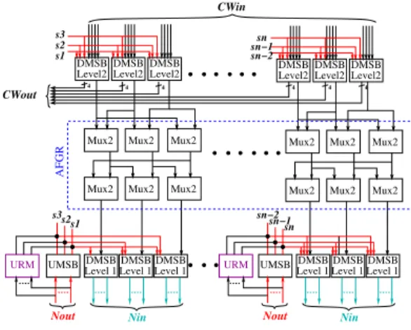
A Switch Box (Sbox)(Fig.3) is composed of UMSBs and DMSBs placed on 2 hierarchical levels (DMSB1 and DMSB2). Each DMSB2 is used to connect Sboxs together and to connect all Sbox’s inputs on DMSB1. Furthermore, DMSB1 has outputs connected to the adjacent clusters (Fig.1). Finally, UMSB connects adjacent cluster outputs to the DMSB1 and DMSB2. Thus, each cluster is connected to adjacent cluster and to adjacent Sbox. This Sbox architecture is generic, each MSB is composed of multiplexers N :1 (Mux) and each multiplexer is composed of multiplexers 2:1 (mux2). There are as many multiplexers (Mux) as MSB’s outputs.
4 4 4 4 4 4 s2 s3 s1 sn−2 sn−1 sn DMSB DMSB DMSB sn s3 s2 s1 sn−2 sn−1 DMSB DMSB DMSB DMSB DMSB DMSB DMSB DMSB DMSB UMSB 2 UMSB 2 2 2 2 1 1 1 2 2 2 1 1 1
Nout Nin Nout Nin
CWin
CWout
Fig. 3: Initial Sbox
III. HARDENING THEFPGA
The next paragraphs review how to adapt for the Sbox the different hardware-based techniques introduced in [17] which are based on hardware redundancy on MSB. To bypass a defect, its location is needed to configure the application. This is done with a map of all defected multiplexers after test and diagnosis [11].
A. Hardware redundancy in Mesh of Clusters architecture In a Mesh of Clusters architecture, if a signal is routed by a defective multiplexer in a MSB, the connection between this signal and its corresponding target is not possible. The presented techniques permit to solve this problem. To adapt the Fine Grain Redundancy technique (FGR) [12] for the Sbox of a Mesh of Clusters architecture, four levels of multiplexers (Mux) are added around all the MSB of the Sbox. As the FGR technique is useless if the nearest multiplexer is already
used by another input, the Improved Fine Grain Redundancy (IFGR) was proposed in [18] to avoid this kind of conflicts. This solution doubles the number of outputs per multiplexer that allows to use the second output in case of defect on the other one. Then, several techniques were proposed in [17] to improve defect tolerance of the cluster : Adapted Fine Grain redundancy (AFGR), Distributed Feedbacks (DF) [11] and Upward Redundant Multiplexer (URM). These techniques can also be applied on the Sbox (Fig.4).
4
Mux2 Mux2 Mux2
Mux2 Mux2 Mux2
Mux2 Mux2 Mux2
Mux2 Mux2 Mux2
4 4 4 4 4
DMSB DMSB DMSB DMSB DMSB DMSB
Level2 Level2 Level2 Level2 Level2 Level2
DMSB DMSB DMSB Level 1 Level 1 Level 1 sn−2 sn−1 sn UMSB s2 s3 s1 DMSB DMSB DMSB UMSB
Level 1 Level 1 Level 1 s3 sn−2 sn−1 sn s1 s2 URM Nout Nin URM Nout Nin AFGR CWout CWin
Fig. 4: Sbox with AFGR, DF and URM [17] The technique called AFGR was proposed to reduce the impact of FGR and IFGR techniques on the FPGA area. This technique consists in removing one of the output multiplexer level to reduce the area overhead and makes the input multi-plexer level common to all DMSBs (Fig.4 shows AFGR on DMSB1). With the technique called Distributed Feedbacks (DF), one or more feedbacks are connected to all DMSBs (as shown in Fig.4 with red bold lines). The technique called Upward Redundant Multiplexers (URM) permits to increase the defect tolerance of UMSBs by adding a multiplexer in parallel to the UMSB (illustrated in Fig.4).
IV. CRITICALITY
Our aim is to measure the impact of each aforementioned technique on the criticality of the different blocks inside the FPGA.
A. Definition
The FPGA can be modeled using a graph G = (N, A) such that :
1) all multiplexers inside the clusters and Sboxs represent the set of nodes N of the graph G.
2) all signals connecting multiplexers represent the set of arcs A such as (x, y) ∈ A.
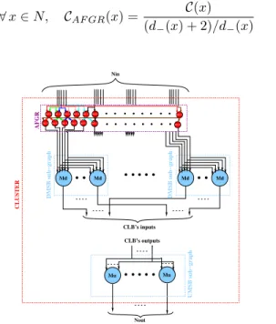
Each cluster and Sbox can be modeled using sub-graphs for DMSBs and UMSBs (illustrated Fig.5 for the cluster). The representation is the same for the Sbox. The criticality C of each node inside the cluster depends on the number of CLBs connected to this node compared to the number of existing paths to through it.
Mu Mu Md Md feedback Md Md feedback CLUSTER Nout Nin CLB’s inputs CLB’s outputs DMSB sub−graph DMSB sub−graph UMSB sub−graph
Fig. 5: Cluster’s nodes
We denote C ⊂ N the set of multiplexers inside the cluster and Dc ⊂ C (resp Uc ⊂ C) the set of multiplexers inside
DMSB (resp. UMSB). Then we have : ∀ x ∈ Dc, C(x) = 1 d+(x) ∗ d−(x) (1) ∀ x ∈ Uc, C(x) = Nclb d+(x) ∗ d−(x) (2) where Nclb represents the number of CLBs per cluster, d+the
number of outputs of this node and d− the number of inputs.
In a cluster of a Mesh of Clusters FPGA, we have :
∀ x ∈ Dc and ∀ y ∈ Uc, d−(x) > d−(y), Nin > Nclb, then
C(x) < C(y).
Similarly, the criticality of each node inside the Sbox depends on the number of inputs/outputs per Sbox compared to the number of existing paths to through it. We denote S ⊂ N the set of multiplexers inside the Sbox and D1s ⊂ S (resp.
D2s⊂ S and Us⊂ S) the set of multiplexers inside the MSBs
(resp. DMSB1, DMSB2 and UMSB2). Then we have : ∀ x ∈ D2s, C(x) = Nout/CWin d+(x) ∗ d−(x) (3) ∀ x ∈ D1s, C(x) = Nout/Nin d+(x) ∗ d−(x) (4) ∀ x ∈ Us, C(x) = Nin− Nout d+(x) ∗ d−(x) (5) where Nin and Nout represents the number of
in-puts/outputs per cluster and CWin the channel width. In a
Sbox of a Mesh of Clusters FPGA, we have :
∀ x ∈ Ds and ∀ y ∈ Us, Nin − Nout > Nout/Nin,
Nin− Nout> Nout/NCW in, d+(x) ∗ d−(x) > d+(y) ∗ d−(y),
then C(x) < C(y).
We can conclude that multiplexers in UMSB are more critical than in DMSB.
B. Impact of redundancy on criticality
1) Classic Fine Grain Redundancy (FGR): With FGR (Fig.6a), the number of outputs per nodes inside DMSB and UMSB increases. In fact, each node can connect all inputs to 3 times more outputs. Then we have :
∀ x ∈ N, CF GR(x) = C(x) 3 (6) OMUX OMUX MSB outputs MSB outputs IMUX IMUX IMUX IMUX IMUX
OMUX
OMUX OMUX OMUX OMUX OMUX OMUX OMUX Md Md OMUX MSB inputs Md Md
IMUX IMUX IMUX IMUX
a−FGR b−IFGR
OMUX
IMUX IMUX IMUX IMUX IMUX
OMUX
OMUX OMUX OMUX OMUX OMUX OMUX OMUX 2 Md Md 2 2 2 OMUX MSB inputs Md Md
IMUX IMUX IMUX IMUX
MSB with FGR sub−graph MSB with IFGR sub−graph
Fig. 6: MSB with FGR and IFGR
2) Improved Fine Grain Redundancy (IFGR): To adapt this technique to the Sbox and cluster architecture, the mul-tiplexer’s outputs inside each MSB are doubled (illustrated in Fig.6b). If the number of outputs per node inside MSBs is doubled, the criticality of each node is divided by 2 compared to FGR. ∀ x ∈ N, CIF GR(x) = CF GR(x) 2 = C(x) 6 (7)
3) Adapted Fine Grain Redundancy (AFGR): With AFGR, the number of inputs per node inside MSBs increases (Fig.7). In fact, each node can use 2 extra inputs from its neighbor. The criticality of each node with AFGR becomes :
∀ x ∈ N, CAF GR(x) = C(x) (d−(x) + 2)/d−(x) (8) Mu Mu Md Md Md Md Nout Nin CLUSTER CLB’s inputs CLB’s outputs IMUXIMUX
IMUXIMUXIMUXIMUXIMUX IMUXIMUXIMUXIMUX
IMUX IMUX IMUX AFGR UMSB sub−graph DMSB sub−graph DMSB sub−graph
Hardware redundancy
technique Sbox criticality Cluster criticality
Mu Md1 Md2 Mu Md
Without redundancy 1(ref) 0.086(ref) 0.033(ref) 1(ref) 0.1(ref)
FGR 0.33(-67%) 0.028(-67%) 0.011(-67%) 0.33(-67%) 0.033(-67%)
IFGR 0.16(-84%) 0.014(-84%) 0.0053(-84%) 0.16(-84%) 0.016(-84%)
AFGR 0.83 (-17%) 0.071(-17%) 0.027(-17%) 0.83 (-17%) 0.083(-17%)
DF 1 (-0%) 0.046(-47%) 0.017 (-47%) 1 (-0%) 0.053 (-47%)
URM 0.01 (-90%) 0.086(-0%) 0.033(-0%) 0.01 (-90%) 0.1 (-0%)
TABLE I: Impact on criticality
4) Distributed Feedbacks (DF): With this technique, the number of inputs per DMSB and per node inside DMSBs increases (Fig.8). The criticality of each node depends on the number of Distributed Feedbacks added (Ndf).
∀ x ∈ Dc∪ D1s∪ D2s, CDF(x) = C(x) (d−(x) + Ndf)/d−(x) (9) Mu Mu Md Md Md Md CLUSTER Nout Nin DF CLB’s inputs CLB’s outputs UMSB sub−graph DMSB sub−graph DMSB sub−graph
Fig. 8: Cluster with DF
5) Upward Redundant Multiplexer (URM): URM tech-nique is applied only on the UMSB and has an impact on the criticality of each node inside UMSB (Fig.9). The criticality of each node depends on the number of URM (Nurm) added
to the UMSB architecture.
∀ x ∈ Uc∪ Us, CU RM(x) =
C(x) 1 + NU RM
(10)
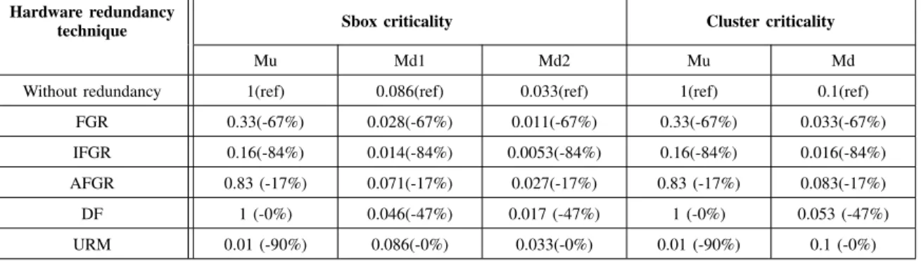
C. Conclusion
In this section, the impact of each technique on the criticality is calculated for a FPGA with a channel width CW in = CW out = 36, a cluster with Nclb = 10, Nin= 24,
Nout = 12 and 4 inputs per CLB. Table I presents the
criticality value using all aforementioned equation depending on the considering node and redundancy technique. In this table, a 1 represents a highly critical block and a 0 a not critical block. Table I shows that without redundancy the most critical blocks are the multiplexers inside UMSBs, then
Mu Mu Md Md feedback Md Md feedback CLUSTER Nout Nin URM CLB’s inputs CLB’s outputs UMSB sub−graph DMSB sub−graph DMSB sub−graph
Fig. 9: Cluster with URM
the multiplexers inside the cluster’s DMSBs. Finally, IFGR technique has the best impact on the DMSB multiplexer criticality (-84%) and URM on the UMSB multiplexer (-90%).
V. EXPERIMENTAL EVALUATIONS
In this section, our objective consists in evaluating the impact of different Local Redundancy Strategy (LRS) on the defect tolerance, area and timing of the FPGA depending on the criticality of the elements of the FPGA. Table I shows that multiplexers inside cluster’s DMSB and multiplexers inside UMSBs are the most critical elements inside a Mesh of Clusters FPGA. IFGR has the best impact on the criticality but the area highly increases [17]. To reduce the area overhead others techniques (FGR, DF and AFGR) with a lowest impact on criticality are used on DMSB. Table II shows 5 different strategies studied in the experiments.
Local Redundancy
Strategies
FGR IFGR AFGR DF URM
LRS1 X X
LRS2 X X
LRS3 X X
LRS4 X X
LRS5 X X
Hardware redundancy
technique
Number of defective multiplexer bypassed in the FPGA
FPGA area overhead
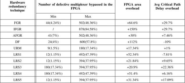
Avg Critical Path Delay overhead Min Max FGR 44(4.24%) 502(48.36%) +64.6% +29.7% IFGR / 878(84.58%) +150% +29.7% AFGR 41(7%) 502(48.36%) +30% +7.46% DF 24(4%) 600(57.8%) +112% -10% URM 9(1.5%) 180(17.34%) +17.34% +1% LRS1 12(1.15%) 492(47.39%) +52.34% -7.81% LRS2 12(1.15%) 394(37.95%) +21.84% +9.65% LRS3 180(17.34%) 394(37.95%) +20.9% +22.36% LRS4 180(17.34%) 492(47.39%) +51.4% +6.16% LRS5 12(1.15%) 394(37.95%) +31.34% +17.09%
TABLE III: Local redundancy techniques performance
A. Methodology
For each 20 MCNC benchmark [19], we determine the smallest architecture in terms of logic blocks number, to place and route all applications. For all simulations, this architecture correspond to a 36x36 FPGA with a channel width of 36, a cluster with 10 CLBs, 24 inputs (6 per crossbar down), 12 outputs. This cluster architecture correspond to the minimal architecture to place and route each benchmark with 10 CLBs per cluster. Then, defects are randomly injected on multiplexers in the FPGA interconnect to make the application not routable. A defect is modeled by undefined value (stuck-open) at the multiplexer output that makes the multiplexer unusable. This number of defective multiplexers corresponds to the defect tolerance of each technique. The number of mux2 added with each technique is compared to initial architecture to evaluate the area increase. Finally, the Critical Path Delay (CPD) of the application is determined for each technique and compared to the initial architecture. For all simulations, we considered that all clusters and Sbox inputs are fault-free. Configuration memory is protected against the defect by using error detection/correction codes [20] [21]. The design under study are the FPGA architecture enriched with all aforementioned strategies : LRS1, LRS2, LRS3, LRS4 and LRS5.
B. Defect tolerance, area and timing results
Table III presents the performance of the different tech-niques in term of tolerance, area and timing. DF, FGR, IFGR, AFGR and URM techniques add extra multiplexers inside all MSBs of the FPGA compared to Local Redundant Strategy (LRS). In fact, with LRS the redundancy is only applied on the most critical elements of the Sbox and cluster. Compared to hardware redundancy techniques, LRS reduces the defect tolerance (-18.65% avg) but the area and the CPD are also reduced (resp -52.58% and -18% avg). We can show that LRS1 and LRS4 techniques permits to bypass a high number of mux2 (47.39%) with a FPGA area overhead of about +52%.
On the contrary with LRS2, LRS3 and LRS5, the impact on the area overhead is reduced (resp. +21.84%, +20.9% and +31.34%) with a less number of multiplexers bypassed (37.95%). In conclusion, using local hardware redundancy on the most critical blocks inside the FPGA permits to tolerate lot of defects with an area overhead reduced compared to an hardware redundancy applied on all the FPGA. For the Critical Path Delay, LRS1 is the best solution (-7.81%) because new paths are added to the cluster that replace defective elements to limit the impact on the Critical Path Delay. Finally, the best trade off is for LRS2 with 37.95% of multiplexers bypassed, an area overhead of +21.84% and an increase of Critical Path Delay of +9.65%.
C. Mesh vs Mesh of Clusters Architecture
0 0,2 0,4 0,6 0,8 1 1 10 100 1000 Y ield
Number of defects (log scale)
Apex redundancy(CG R)(32x32) Apex redundancy (CGR)(256x256) FGR mesh(32x32) FGR mesh(256x256) LRS1 Mesh of Clusters(36x36) LRS2 Mesh of Clusters(36x36) LRS3 Mesh of Clusters(36x36) LRS4 Mesh of Clusters(36x36)
Fig. 10: Impact on FPGA yield
In this paragraph, we compared the FPGA yield to the number of defects (Fig.10) and timing (Fig.11) for industrial mesh FPGA [12] [13] with different redundancy techniques (FGR, IFGR) and all presented techniques on our Mesh of Clusters architecture using local redundancy strategies (LRS1, LRS2, LRS3, LRS4 and LRS5). The yield represents the
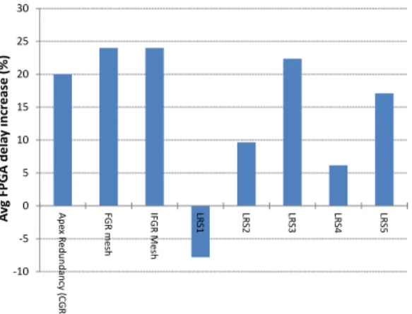
FPGA functionality after manufacturing. It shows that all tech-niques using local redundancy applied on a Mesh of Clusters architecture permits to tolerate around 4 times more defects than FGR,IFGR, CGR applied on a mesh-based industrial FGPA interconnect [12] [13] [9]. We can also compare all techniques using local redundancy applied on Mesh of Clusters architecture. Best results are obtained using LRS1 and LRS4 with around 492 defects tolerated. Finally, LRS2, LRS3 and LRS5 have the same impact with 394 defects tolerated. Fig.11, shows the impact of each method on the average Critical Path Delay overhead when local hardware redundancy is applied. Each proposed methods (LRS1, LRS2, LRS3, LRS4 and LRS5) reduce the CPD overhead compared to FGR and IFGR because, the hardware redundancy is not applied on the total FPGA architecture to limit the area overhead. As mentioned before LRS1 is the best solution (-7.81%). Finally, LRS permits the designer to fix a trade off between area, defect tolerance or delay. -10 -5 0 5 10 15 20 25 30 Ape x R edun dan cy (C GR) FGR mesh IF GR Mesh LRS1 LRS2 LRS3 LRS4 LRS5 A vg FPGA dela y incr ease ( %)
Fig. 11: Impact on Critical Path Delay
VI. CONCLUSION AND FUTURE WORK
In this paper, we determined the most critical blocks inside the FPGA to applied different local hardware redundancy strategies to the Mesh of Clusters topology. It permits to tolerate 4 times more defects than a classic hardware re-dundancy applied in a mesh architecture. Each method uses hardware redundancy in the FPGA local interconnect. How-ever our investigation indicates that the choice of defect tolerant techniques has a significant impact on area and critical path delay. With these strategies, we obtain the best trade off between the number of defects bypassed (37.95%), the FPGA area overhead (21.84%) and critical path delay (9.65%). Furthermore, with our techniques the designer can choose his trade off between area, defect tolerance or delay. For future works, it will be interesting to study the impact of Coarse Grain Redundancy techniques.
ACKNOWLEDGMENT
This work is a part of the project Robust FPGA ANR 11 INS-02, funded by The French National Research Agency, The Pole Systematic and The Pole Minalogic.
REFERENCES
[1] Rahul Jain, Anindita Mukherjee, and Kolin Paul. Defect-aware design paradigm for reconfigurable architectures. In IEEE Computer Society Annual Symposium on Emerging VLSI Technologies and Architectures, pages 6–pp. IEEE, 2006.
[2] Honey Goel and Daren Dance. Yield enhancement challenges for 90 nm and beyond. In Advanced Semiconductor Manufacturing Conference and Workshop, 2003 IEEEI/SEMI, pages 262–265. IEEE, 2003. [3] Helia Naeimi and Andr´e DeHon. A greedy algorithm for tolerating
defective crosspoints in nanopla design”. In International Conference on Field-Programmable Technology, pages 49–56. IEEE, 2004. [4] Nicola Campregher, Peter YK Cheung, George A Constantinides, and
Milan Vasilko. Analysis of yield loss due to random photolithographic defects in the interconnect structure of fpgas. In Proceedings of the 2005 ACM/SIGDA 13th international symposium on Field-programmable gate arrays, pages 138–148. ACM, 2005.
[5] Vijay Lakamraju and Russell Tessier. Tolerating operational faults in cluster-based fpgas. In Proceedings of the 2000 ACM/SIGDA eighth international symposium on Field programmable gate arrays, pages 187–194. ACM, 2000.
[6] Abderrahim Doumar, Satoshi Kaneko, and Hideo Ito. Defect and fault
tolerance fpgas by shifting the configuration data. In International
Symposium on Defect and Fault Tolerance in VLSI Systems. DFT’99, pages 377–385. IEEE, 1999.
[7] San Jose CA Xilinx. Easypath solutions. In http://www.xilinx.com/
products/easypath/, 2005.
[8] Raphael Rubin and Andr´e DeHon. Choose-your-own-adventure routing: lightweight load-time defect avoidance. ACM Transactions on Recon-figurable Technology and Systems (TRETS), 4(4):33, 2011.
[9] Altera Corporation. Apex redundancy. In
http://www.altera.com/products /devices/apex/features/apx-redundancy, 2005.
[10] John D. Corbett Xilinx. The xilinx isolation design flow for fault-tolerant systems. In http://www.xilinx.com/support/documentation/white papers /wp412 IDF for Fault Tolerant, 2012.
[11] A. Ben Dhia, S. Ur Rehman, A. Blanchardon, L. Naviner, M. Benab-denbi, R. Chotin-Avot, H. Mehrez, E. Amouri, and Z. Marrakchi. A defect-tolerant cluster in a mesh sram-based fpga. In in FPT, Kyoto, Japan, pp. 434-437 (2013).
[12] AJ Yu and Guy G Lemieux. Fpga defect tolerance: Impact of granularity. In International Conference on Field-Programmable Technology, pages 189–196. IEEE, 2005.
[13] AJ Yu and Guy GF Lemieux. Defect-tolerant fpga switch block and connection block with fine-grain redundancy for yield enhancement. In International Conference on Field Programmable Logic and Applica-tions, pages 255–262. IEEE, 2005.
[14] E. Amouri, A. Blanchardon, R. Chotin-Avot, H. Mehrez, and Z.
Mar-rakchi. Efficient multilevel interconnect topology for cluster-based
mesh fpga architecture. In International Conference on ReConFigurable Computing and FPGAs, 2013.
[15] Andre DeHon. Reconfigurable architectures for general-purpose com-puting. 1996.
[16] Joachim Pistorius and Mike Hutton. Placement rent exponent calcu-lation methods, temporal behaviour and fpga architecture evaluation. In Proceedings of the 2003 international workshop on System-level interconnect prediction, pages 31–38. ACM, 2003.
[17] A. Blanchardon, R. Chotin-Avot, H. Mehrez, and E. Amouri. Improve defect tolerance in a cluster of a sram-based mesh of cluster fpga using hardware redundancy. In in FPL, Munich, Germany, 201.
[18] AJ Yu and Guy GF Lemieux. Defect-tolerant fpga switch block and connection block with fine-grain redundancy for yield enhancement. In International Conference on Field Programmable Logic and Applica-tions, pages 255–262. IEEE, 2005.
[19] Lgsynth93 benchmark set: Version 4.0. In Technical report, Collabora-tive Benchmarking Laboratory, 1993.
[20] Charles W Slayman. Cache and memory error detection, correction, and reduction techniques for terrestrial servers and workstations. IEEE Transactions on Device and Materials Reliability, 5(3):397–404, 2005. [21] Fabrice Monteiro, Stanislaw J Piestrak, Houssein Jaber, and Abbas Dandache. Fault-secure interface between fault-tolerant ram and
trans-mission channel using systematic cyclic codes. In On-Line Testing
Symposium, 2007. IOLTS 07. 13th IEEE International, pages 199–200. IEEE, 2007.