HAL Id: hal-00991841
https://hal.archives-ouvertes.fr/hal-00991841
Submitted on 16 May 2014
HAL is a multi-disciplinary open access archive for the deposit and dissemination of sci-entific research documents, whether they are pub-lished or not. The documents may come from
L’archive ouverte pluridisciplinaire HAL, est destinée au dépôt et à la diffusion de documents scientifiques de niveau recherche, publiés ou non, émanant des établissements d’enseignement et de
Polarization-insensitive wavelength conversion of 40
Gb/s NRZ-DPSK signals in a silicon polarization
diversity circuit
Dragana Vukovic, Yunhong Ding, Hao Hu, Haiyan Ou, Leif Katsuo Oxenløwe,
Christophe Peucheret
To cite this version:
Dragana Vukovic, Yunhong Ding, Hao Hu, Haiyan Ou, Leif Katsuo Oxenløwe, et al.. Polarization-insensitive wavelength conversion of 40 Gb/s NRZ-DPSK signals in a silicon polarization diversity circuit. Optics Express, Optical Society of America - OSA Publishing, 2014, 22 (10), pp.12467-12474. �10.1364/OE.22.012467�. �hal-00991841�
Polarization-insensitive wavelength conversion
of 40 Gb/s NRZ-DPSK signals in a silicon
polarization diversity circuit
Dragana Vukovic,1,* Yunhong Ding,1 Hao Hu,1Haiyan Ou,1 Leif Katsuo Oxenløwe,1 and Christophe Peucheret1,2
1Department of Photonics Engineering, Technical University of Denmark, DK-2800 Kgs. Lyngby, Denmark 2FOTON Laboratory, CNRS UMR 6082, ENSSAT, University of Rennes 1, 22305 Lannion, France
*drvu@fotonik.dtu.dk
Abstract: Polarization insensitive wavelength conversion of a 40 Gb/s non-return-to-zero (NRZ) differential phase-shift keying (DPSK) data signal is demonstrated using four-wave mixing (FWM) in a silicon nanowire circuit. Polarization independence is achieved using a diversity circuit based on polarization rotators and splitters, which is fabricated by a simple process on the silicon-on-insulator (SOI) platform. Error-free performance is achieved with only 0.5 dB of power penalty compared to the wavelength conversion of a signal with well optimized input polarization. Additionally, data transmission over 161 km standard single-mode fiber (SSMF) is demonstrated at 40 Gb/s using optical phase conjugation (OPC) in the proposed circuit.
©2014 Optical Society of America
OCIS codes: (130.7405) Wavelength conversion devices; (070.4340) Nonlinear optical signal
processing; (190.4380) Nonlinear optics, four-wave mixing. References and links
1. B. Ramamurthy and B. Mukherjee, “Wavelength conversion in WDM networking,” IEEE J. Sel. Areas Comm.
16(7), 1061–1073 (1998).
2. K. Inoue and H. Toba, “Wavelength conversion experiment using fiber four-wave mixing,” IEEE Photon. Technol. Lett. 4(1), 69–72 (1992).
3. G.-W. Lu, T. Sakamoto, and T. Kawanishi, “Wavelength conversion of optical 64QAM through FWM in HNLF and its performance optimization by constellation monitoring,” Opt. Express 22(1), 15–22 (2014).
4. K. Inoue, “Polarization independent wavelength conversion using fiber four-wave mixing with two orthogonal pump lights of different frequencies,” J. Lightwave Technol. 12(11), 1916–1920 (1994).
5. T. Hasegawa, K. Inoue, and K. Oda, “Polarization independent frequency conversion by fiber four-wave mixing with a polarization diversity technique,” IEEE Photon. Technol. Lett. 5(8), 947–949 (1993).
6. J. Lu, L. Chen, Z. Dong, Z. Cao, and S. Wen, “Polarization insensitive wavelength conversion based on orthogonal pump four-wave mixing for polarization multiplexing signal in high-nonlinear fiber,” J. Lightwave Technol. 27(24), 5767–5774 (2009).
7. W. Astar, A. S. Lenihan, and G. M. Carter, “Polarization-insensitive wavelength conversion by FWM in a highly nonlinear PCF of polarization-scrambled 10-Gb/s RZ-OOK and RZ-DPSK signals,” IEEE Photon. Technol. Lett.
19(20), 1676–1678 (2007).
8. M. F. Huang, J. Yu, Y. K. Huang, E. Ip, and G. K. Chang, “Wavelength converter for polarization-multiplexed 100-G transmission with multilevel modulation using a bismuth oxide-based nonlinear fiber,” IEEE Photon. Technol. Lett. 22(24), 1832–1834 (2010).
9. J. M. Tang and K. A. Shore, “A simple scheme for polarization insensitive four-wave mixing in semiconductor optical amplifiers,” IEEE Photon. Technol. Lett. 11(9), 1123–1125 (1999).
10. C. M. Gallep, O. Raz, and H. J. S. Dorren, “Polarization independent dual wavelength converter based on FWM in a single semiconductor optical amplifier,” in Optical Fiber Communication Conference, OFC 2010, paper OWP2.
11. I. Brener, M. H. Chou, E. Chaban, K. R. Parameswaran, M. M. Fejer, S. Kosinski, and D. L. Pruitt, “Polarisation-insensitive wavelength converter based on cascaded nonlinearities in LiNbO3 waveguides,”
12. S. L. Jansen, D. Van den Borne, B. Spinnler, S. Calabro, H. Suche, P. M. Krummrich, W. Sohler, G.-D. Khoe, and H. de Waardt, “Optical phase conjugation for ultra long-haul phase-shift-keyed transmission,” J. Lightwave Technol. 24(1), 54–64 (2006).
13. P. Martelli, P. Boffi, M. Ferrario, L. Marazzi, P. Parolari, R. Siano, V. Pusino, P. Minzioni, I. Cristiani, C. Langrock, M. M. Fejer, M. Martinelli, and V. Degiorgio, “All-optical wavelength conversion of a 100-Gb/s polarization-multiplexed signal,” Opt. Express 17(20), 17758–17763 (2009).
14. H. Hu, R. Nouroozi, R. Ludwig, B. Huettl, C. Schmidt-Langhorst, H. Suche, W. Sohler, and C. Schubert, “Polarization-insensitive all-optical wavelength conversion of 320 Gb/s RZ-DQPSK signals using a Ti:PPLN waveguide,” Appl. Phys. B 101(4), 875–882 (2010).
15. S. Gao, X. Zhang, Z. Li, and S. He, “Polarization-independent wavelength conversion using an angled-polarization pump in a silicon nanowire waveguide,” IEEE J. Sel. Top. Quantum Electron. 16(1), 250–256 (2010).
16. M. Pu, H. Hu, C. Peucheret, H. Ji, M. Galili, L. K. Oxenløwe, P. Jeppesen, J. M. Hvam, and K. Yvind, “Polarization insensitive wavelength conversion in a dispersion-engineered silicon waveguide,” Opt. Express
20(15), 16374–16380 (2012).
17. T. Barwicz, M. R. Watts, M. A. Popovic, P. T. Rakich, L. Socci, F. X. Kartner, E. P. Ippen, and H. I. Smith, “Polarization-transparent microphotonic devices in the strong confinement limit,” Nat. Photonics 1(1), 57–60 (2007).
18. Y. Ding, L. Liu, C. Peucheret, J. Xu, H. Ou, K. Yvind, X. Zhang, and D. Huang, “Towards polarization diversity on the SOI platform with simple fabrication process,” IEEE Photon. Technol. Lett. 23(23), 1808–1810 (2011). 19. Y. Ding, B. Huang, H. Ou, F. Da Ros, and C. Peucheret, “Polarization diversity DPSK demodulator on the
silicon-on-insulator platform with simple fabrication,” Opt. Express 21(6), 7828–7834 (2013).
20. H. Fukuda, K. Yamada, T. Tsuchizawa, T. Watanabe, H. Shinojima, and S. Itabashi, “Silicon photonic circuit with polarization diversity,” Opt. Express 16(7), 4872–4880 (2008).
21. Y. Ding, H. Ou, and C. Peucheret, “Wideband polarization splitter and rotator with large fabrication tolerance and simple fabrication process,” Opt. Lett. 38(8), 1227–1229 (2013).
22. D. Dai and J. E. Bowers, “Novel concept for ultracompact polarization splitter-rotator based on silicon nanowires,” Opt. Express 19(11), 10940–10949 (2011).
23. Y. Ding, J. Xu, F. Da Ros, B. Huang, H. Ou, and C. Peucheret, “On-chip two-mode division multiplexing using tapered directional coupler-based mode multiplexer and demultiplexer,” Opt. Express 21(8), 10376–10382 (2013).
24. M. Pu, L. Liu, H. Ou, K. Yvind, and J. M. Hvam, “Ultra-low-loss inverted taper coupler for silicon-on-insulator ridge waveguide,” Opt. Commun. 283(19), 3678–3682 (2010).
25. Y. Ding, H. Ou, and C. Peucheret, “Ultrahigh-efficiency apodized grating coupler using fully etched photonic crystals,” Opt. Lett. 38(15), 2732–2734 (2013).
1. Introduction
All-optical wavelength converters (AOWCs) are key components to be employed in wavelength division multiplexing (WDM) optical communication systems in order to enable routing or resolve traffic bottleneck issues in networks nodes [1]. Modern optical networks require those components to have an ultra-fast response in order to process high-speed data signals. Furthermore, they should be suitable for processing signals employing phase modulation or high-order modulation formats utilizing the phase dimension, such as quadrature amplitude modulation. These two conditions can be fulfilled if all-optical signal processing relies on four-wave mixing (FWM). Consequently, AOWCs based on FWM have been widely investigated [2] and have regained interest over the past decade in the context of the conversion of advanced optical modulation formats [3].
However, the FWM process being strongly polarization-dependent, it requires a precise control of the states-of-polarization (SOPs) of the interacting waves (pumps and signal to convert), which is difficult to ensure in a real network node where the SOP of the signal may fluctuate randomly with time after propagation over an optical fiber link. Polarization-insensitive operation is therefore a required feature for the practical deployment of FWM-based wavelength converters. The problem is well known when optical fibers are used as the nonlinear medium and solutions based on either dual orthogonal pumps [4] or on a polarization diversity loop [5] have been proposed and routinely investigated over a variety of fiber types, including silica highly nonlinear fibers (HNLFs) [6], photonic crystal fibers (PCFs) [7], and bismuth-oxide HNLFs [8].
Being able to fabricate compact AOWCs is essential if they are to be used in optical cross-connects or other network elements with large channel counts. At the device level,
polarization-insensitive wavelength conversion has been demonstrated in semiconductor optical amplifiers (SOAs) [9,10] and periodically-poled lithium niobate (PPLN) waveguides [11–14]. Recently, polarization-insensitive wavelength conversion has also been described [15] and demonstrated in silicon waveguides [16], which constitute a very promising nonlinear platform thanks to their high nonlinear coefficients and strong confinement allowing compact-size devices to be fabricated, as well as their compatibility with complementary metal-oxide-semiconductor (CMOS) fabrication technology, enabling device integration. The drawback of the angle-pump scheme applied in [16] is the fact that the waveguides should be engineered so that they have similar dispersive properties for the TE and TM modes, which may restrict the possibilities to simultaneously achieve a large conversion bandwidth and high conversion efficiency (CE). Alternatively, the conversion bandwidth will be limited by that of the polarization mode that has the narrower bandwidth.
The polarization diversity (Pol-D) technique based on polarization splitters and rotators (PSRs) [17–20] has been demonstrated to be an efficient mean to reduce the polarization dependence of passive integrated circuits. In this paper, we propose and demonstrate on-chip polarization insensitive wavelength conversion using a Pol-D circuit for the first time. Since only one polarization needs to be processed after the first PSR, the scheme offers more freedom for dispersion engineering of the nonlinear silicon nano-waveguide in order to obtain broad-band high-efficiency wavelength conversion. Polarization-insensitive wavelength conversion is demonstrated for a 40 Gb/s non-return-to-zero differential phase-shift keying (NRZ-DPSK) data signal. Error-free performance of the converted signal is achieved with only 0.5 dB of power penalty at a bit-error-ratio (BER) of 10−9 compared to the case of an idler generated from an input signal with optimized fixed state-of-polarization. In addition, since the FWM conversion also realizes phase conjugation, a 40 Gb/s NRZ-DPSK signal is successfully transmitted over 161 km standard single-mode fiber (SSMF) using dispersion compensation by mid-span spectral inversion, thus demonstrating an application that requires polarization-insensitive operation.
2. Principle, design, and fabrication of the Pol-D circuit
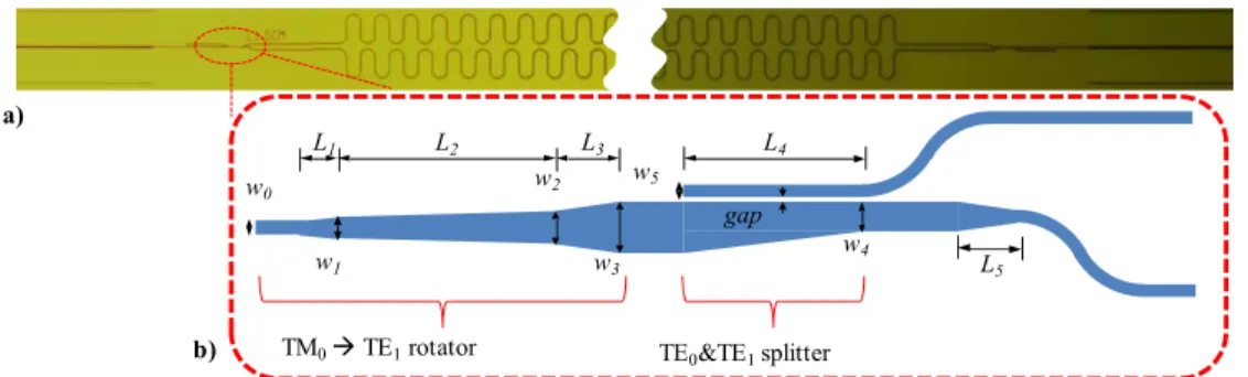
To achieve polarization-insensitive wavelength conversion, a silicon Pol-D circuit based on a PSR has been designed. The Pol-D circuit consists of two PSRs at the input and output of the chip that are linked by two identical Si nano-waveguides. The width, height and length of the waveguides were designed to be 500 nm, 250 nm and 1.5 cm, respectively. The 1.5 cm long waveguide consists of 90° bend sections with bend radius of 25 µm and straight sections. The first PSR splits the input TE0 and TM0 modes into two TE0 beams propagating in the two Si nano-waveguides. At the output of the waveguides, the two TE0 beams are combined back via the second PSR at the chip output. It should be noticed that the second PSR is flipped with respect to the first PSR, resulting in a low polarization dependent loss (PDL) for the whole circuit, regardless of the PDL value of the PSR itself. As a result, the total device exhibits a polarization independent transmission. The PSR is based on a tapered waveguide TM0-to-TE1 mode converter [21,22] followed by a tapered directional coupler (DC)-based TE0&TE1 mode splitter [23], as shown in Fig. 1(b). In the case of TE0 input, the light will propagate through the adiabatic taper without any change, while in the case of TM0 input the light will be converted to the TE1 mode during the adiabatic tapering [21,22]. In this design, air is employed as top cladding material to achieve an efficient TM0 to TE1 polarization rotation. The tapered waveguide is divided into three sections, starting from a single mode silicon waveguide with a width of w0 = 450 nm to w1 = 650 nm, and length of L1 = 10 μm, then a second tapering section from w1 to w2 = 750 nm with length of L2 = 150 μm, and finally a section from w2 to w3 = 850 nm with a tapering length L3 = 10 μm [21]. The TM0-to-TE1 mode converter is followed by a fabrication tolerant TE0&TE1 mode splitter [23] which consists of a narrow silicon waveguide 390 nm wide (w5), parallel-coupled with another wide tapered waveguide tapered from 850 nm down to 750 nm (w4). The coupling gap and length
(L4) are 100 nm and 30 μm, respectively. The two output ports of the TE0&TE1 mode splitter are finally both tapered to 500 nm with tapering length L5 of 10 µm, and connected to the two identical nonlinear silicon waveguides. All the details are shown in Fig. 1(b).
The entire circuit was fabricated on an SOI wafer with 250 nm top silicon layer and 3 μm buried silicon dioxide layer using a single step of E-beam lithography and inductively coupled plasma reactive ion etching. More details on the fabrication and design can be found in [19,21]. The input and output ports of the circuit were also equipped with silicon inverse tapers in order to reduce coupling loss to tapered fibers to 1.5 dB/facet. A microscope image of the whole device is shown in Fig. 1(a). The total insertion loss of the fabricated device was measured to be 13 dB with PDL lower than 1 dB. Considering coupling loss of 3 dB for the two facets and typical propagation loss of 4.2 dB/cm for the nonlinear silicon waveguides [25], the loss of each PSR was estimated to be around 1.6 dB.
b) a) w0 w1 w2 w3 L1 L2 L3 L4 L5 w4 w5 gap
TM0 TE1rotator TE0&TE1splitter
Fig. 1. (a) Microscope image of the whole polarization insensitive wavelength converter. (b) Schematic structure of the PSR.
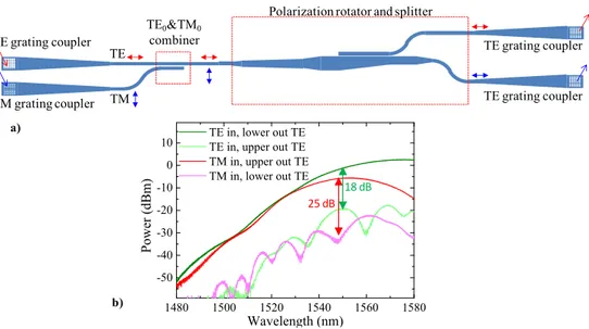
In order to measure the polarization properties of the fabricated PSR, a separate device was fabricated, as shown schematically in Fig. 2(a). This test device consists of two fully etched apodized TE and TM input grating couplers [24] followed by a directional coupler-based mode combiner. After being combined, both modes are passing through the same well-designed PSR as the one used in the Pol-D circuit and are out-coupled using two TE grating couplers. Figure 2(b) shows the measured transmission from TE and TM inputs to the TE outputs and the corresponding modal crosstalk, from the TE input to the lower TE output as well as from the TM input to the upper TE output. Polarization crosstalk lower than –18 dB and −25 dB are obtained for TE and TM inputs, respectively. The crosstalk induced by residual TM light is not shown in Fig. 2(b). However, it is negligible since a 150 µm long tapering length for the TM0-TE1 mode converter can guarantee a conversion efficiency higher than 99% [21].
3. Wavelength conversion experiment
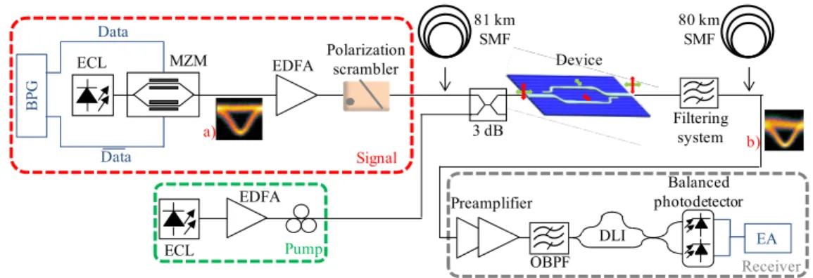
The experimental setup for polarization-insensitive wavelength conversion is shown in Fig. 3. The data signal was generated starting from a continuous wave (CW) external cavity laser (ECL) at 1549 nm and modulated in the DPSK format at 40 Gb/s using a standard Mach-Zehnder modulator (MZM) driven in push-pull operation by an NRZ pseudo-random binary sequence (PRBS) of length 215−1. The data signal was further amplified in an erbium-doped fiber amplifier (EDFA) such that the signal power at the input of the device was around 15 dBm.
TE0&TM0
combiner
Polarization rotator and splitter TE grating coupler
TM grating coupler
TE TE grating coupler
TE grating coupler TM
TE in, lower out TE TE in, upper out TE TM in, upper out TE TM in, lower out TE
1480 1500 1520 1540 1560 1580 -50 -40 -30 -20 -10 0 10 Power (dBm) Wavelength (nm) b) a) 18 dB 25 dB
Fig. 2. (a) Schematic structure of the device used for the characterization of the PSR. (b) Measured coupling efficiencies to the two output ports for TE0 and TM0 inputs.
In order to test the polarization sensitivity, the SOP of the signal was continuously changed using a polarization scrambler (PS).A CW pump was generated from an ECL at 1551 nm and amplified with another EDFA, leading to 21 dBm pump power at the input of the device. The separation between pump and signal was only 2 nm, leading to about 4 nm separation between signal and idler. However, this separation can be further increased since a large working bandwidth is expected for this type of PSR [22]. Within this bandwidth the conversion efficiency will be determined by phase-matching considerations, hence by the dispersion properties of the nonlinear waveguides. The SOP of the pump was adjusted using a polarization controller. The signal and pump were combined by a 3 dB coupler before being coupled into the device. Tapered fibers were used for coupling light in and out of the Pol-D wavelength converter. The total power at the input of the device was 22 dBm, leading to a slightly higher insertion loss of 15 dB compared to the linear case, caused by increased nonlinear losses in the waveguides. The optimum pump polarization was determined by minimizing the power variations of the idler when changing the polarization of the input signal. The minimum variation of the idler power was estimated to be around 2 dB. This optimization can also be performed simply by optimizing the eye diagram of the converted signal. After the device, the generated idler was filtered using three optical bandpass filters (OBPFs) of 3 nm, 1 nm and 0.8 nm bandwidths with an EDFA in between the second and third OBPF. The filtered idler was further input into a pre-amplified balanced receiver. The receiver consists of a 25 ps fiber delay line interferometer (DLI) and a balanced photodetector with 45 GHz bandwidth in order to perform demodulation and detection of the DPSK idler. The demodulated idler was further sent to a 40 Gb/s error analyzer (EA) for BER measurements.
In the transmission experiment, the generated signal was first transmitted over 81 km SSMF and coupled into the silicon chip together with the CW pump. The generated idler was filtered, amplified and transmitted over another 80 km SSMF span. Since the signal and idler have different wavelengths, they do not experience the same total accumulated dispersion in the fibers before and after the OPC, hence the choice of slightly different fiber lengths in the first and second transmission spans. The power levels of the signal and the pump at the input of the device were kept the same as in the wavelength conversion experiment. The transmission spans were placed before and after the wavelength converter, as indicated with arrows in Fig. 3.
ECL MZM Filtering system 3 dB EDFA BP G Polarization scrambler ECL EDFA Data Data OBPF Balanced photodetector EA DLI Preamplifier Receiver Signal Pump 81 km SMF a) b) 80 km SMF Device
Fig. 3. Experimental setup for polarization-insensitive wavelength conversion. Insets a) and b) show the eye diagrams of the signal at the transmitter output and of the converted idler, respectively. 81 km and 80 km SSMF were added before and after the wavelength converter in the mid-span spectral inversion experiment.
3.1 Experimental results
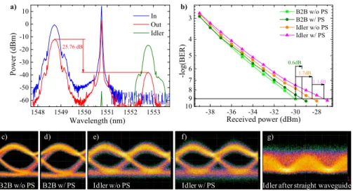
The spectra at the input and output of the device, as well as the spectrum of the filtered and amplified idler are shown in Fig. 4(a). For 21 dBm input pump power, the measured conversion efficiency, defined as the ratio between the idler power and the signal power at the output of the device, was measured to be −25.8 dB. All the spectra were saved while the polarization of the input signal was being scrambled. By switching off the polarization scrambler and optimizing the SOP of the signal to maximize the CE, a value of –23.5 dB was obtained. The performance of the converted signal (idler) was investigated through BER measurements as a function of the average received power, as shown in Fig. 4(b). Back to back (B2B) performances measured at the output of the MZM are compared with the BER of the converted signal when the input signal polarization was optimized and when it was scrambled. Error-free performance was achieved in both cases. The power penalty at a BER of 10−9 compared to the back-to-back case originating from the whole wavelength conversion scheme was 1.7 dB when the input signal had an optimized fixed input polarization. This power penalty caused by a reduced optical signal-to-noise ratio (OSNR) at the output of the converter could be decreased by having a higher conversion efficiency, which could be obtained using a higher input pump power. The reduction in idler sensitivity caused by polarization scrambling was additionally 1.1 dB. However, measuring the performance of the back-to-back signal after scrambling revealed a penalty of 0.6 dB compared to the fixed polarization case, due to a small polarization dependence in the receiver. Taking this penalty into account indicates that actually only 0.5 dB of penalty is caused by the imperfection of the PSR. As it can be seen in Fig. 2(b), the maximum polarization crosstalk between the two outputs of the PSR at 1550 nm was around –18 dB, which may cause this small power penalty. The polarization crosstalk could be improved by increasing the length of the adiabatic taper-based TM0-TE1 converter to obtain a higher mode extinction ratio. Clear and open eye diagrams of the demodulated converted signals in Figs. 4(e) and 4(f) show very small distortion compared with the eye diagrams of the corresponding demodulated input signals shown in Figs. 4(c) and 4(d) (without and with polarization scrambling, respectively). On the other hand, error free performance could not be achieved when the polarization scrambler was used with a single 1 cm long waveguide of the same design but without PSRs, as can be seen from the closed eye diagram in Fig. 4(g), showing the effectiveness of the demonstrated Pol-D scheme. The eye closure is clearly due to the action of the polarization scrambler and not to the fact that the reference waveguide is shorter, since approximately the same conversion efficiency as with the 1.5 cm waveguide with PSRs was measured.
Results obtained in the transmission experiment are shown in Fig. 5. The BER curves in Fig. 5(a) correspond to the back-to-back case, the case with wavelength conversion alone,
B2B w/o PS B2B w/ PS Idler w/o PS Idler w/ PS -38 -36 -34 -32 -30 -28 10 9 8 7 6 5 4 3 -lo g(BER) Received power (dBm) 0.6dB 1.7dB 1.1dB In Out Idler 1548 1549 1550 1551 1552 1553 -60 -50 -40 -30 -20 -10 0 10 Pow er (dBm ) Wavelength (nm) 25.76 dB
B2B w/o PS Idler w/o PS Idler w/ PS
c) e) f)
a) b)
Idler after straight waveguide g)
d)
B2B w/ PS
Fig. 4. (a) Spectra at the input and output of the device and spectrum of the filtered and amplified idler. (b) Bit-error-ratio (BER) curves for the back-to-back (B2B) and wavelength converted 40 Gb/s DPSK signals with optimized polarization and with the polarization scrambler (PS) turned on. Eye diagrams of the demodulated (c) non-scrambled B2B signal, (d) scrambled B2B signal, (e) idler when the input signal is not scrambled, and (f) idler when the input signal is scrambled. All eye diagrams are recorded for −29 dBm received power. (g) Eye
diagram of the idler converted in a straight 1 cm long silicon waveguide when the state-of-polarization of the input signal is scrambled.
and the case with transmission over 161 km SSMF and mid-span spectral inversion All cases are investigated for non-scrambled and scrambled data signals with a 27–1 long PRBS. Transmission over 161 km SSMF of the non-scrambled signal leads to an additional 1.3 dB penalty compared to the case with wavelength converter only. When the signal is scrambled, a penalty of 3.6 dB is observed. Additional penalty is introduced during the transmission due to the reduced OSNR combined with imperfections of the Pol-D circuit when the transmitted signal is scrambled. However, error free transmission is demonstrated, which is also seen from the open eye diagrams shown in Fig. 5(b) and 5(c) for non-scrambled and scrambled signal at the input of the link, respectively. The eye diagram in Fig. 5(d) represents a signal without phase conjugation after transmission over only 81 km SSMF.
B2B w/o PS B2B w/ PS Idler w/o PS Idler w/ PS Transmission w/o PS Transmission w/ PS -38 -36 -34 -32 -30 -28 -26 -24 10 9 8 7 6 5 4 3 -l og( B E R ) Received power (dBm) 1.3dB 3.6dB Transmission w/o PS
Transmission w/o OPC b)
d)
a)
c)
Transmission w/ PS
Fig. 5. (a) Bit-error-ratio (BER) curves for the transmission of a 40 Gb/s DPSK signal over 161 km SMF with and without polarization scrambler (PS) at the link input. Eye diagrams after transmission of the demodulated signals without (b) and with (c) polarization scrambler at the link input. Both eye diagrams are recorded for −25 dBm received power. (d) Eye diagram of a
4. Conclusions
We have demonstrated polarization-independent wavelength conversion of a 40 Gb/s NRZ-DPSK signal using FWM in a silicon device. The fabricated device shows polarization independent transmission thanks to a circuit which consists of two identical PSRs and two identical Si nano-waveguides where FWM occurs. Error-free performance is achieved for the wavelength converted signal when the input signal polarization is scrambled. Furthermore, taking advantage of the optical phase conjugation occurring during the wavelength conversion process, a 40 Gb/s NRZ-DPSK data signal was successfully transmitted over 161 km SSMF while being polarization-scrambled at the link input, achieving error free performance.
Acknowledgments
This work was supported by Villum Fonden through the “Nanophotonics for Terabit Communications” (NATEC) Centre and the Danish Council for Independent Research (project DFF – 1337-00152).