HAL Id: hal-00490938
https://hal.archives-ouvertes.fr/hal-00490938
Submitted on 10 Jun 2010
HAL is a multi-disciplinary open access
archive for the deposit and dissemination of
sci-entific research documents, whether they are
pub-lished or not. The documents may come from
teaching and research institutions in France or
abroad, or from public or private research centers.
L’archive ouverte pluridisciplinaire HAL, est
destinée au dépôt et à la diffusion de documents
scientifiques de niveau recherche, publiés ou non,
émanant des établissements d’enseignement et de
recherche français ou étrangers, des laboratoires
publics ou privés.
Design of InGaAs/InP 1.55µm vertical cavity surface
emitting lasers
Jean-Michel Lamy, Cyril Paranthoen, Christophe Levallois, Soline Richard,
Hervé Folliot, Nicolas Chevalier, Alain Le Corre, Slimane Loualiche
To cite this version:
Jean-Michel Lamy, Cyril Paranthoen, Christophe Levallois, Soline Richard, Hervé Folliot, et al..
De-sign of InGaAs/InP 1.55µm vertical cavity surface emitting lasers. International Conference on
Nu-merical Simulation of Optoelectronic Devices (NUSOD ’08), Sep 2008, Nottingham, United Kingdom.
p 1-2, �10.1109/NUSOD.2008.4668208�. �hal-00490938�
DESIGN OF InGaAs/InP 1.55µm VERTICAL
CAVITY SURFACE EMITTING LASERS
J.-M. Lamy, C. Paranthoën, C. Levallois, S. Richard, H. Folliot, N. Chevalier, A. Le Corre, S. Loualiche
UMR FOTON 6082 CNRS, INSA de Rennes, Campus Beaulieu, 35043 Rennes Cedex, FranceSoline.richard@insa-rennes.fr
Abstract-The design of an electrically pumped InGaAs quantum
well based vertical cavity surface emitting laser (VCSEL) on InP substrate is presented. Such optically pumped VCSELs have already been demonstrated. To design electrically pumped VCSEL, three simulations steps are needed: optical simulation gives access to the electric field repartition, to design the active zone and the Bragg mirrors. Thermal simulation is helpful to design metallic contacts while the energy band diagram is obtained by electrical simulation to design the buried tunnel junction useful for carrier injection. All these simulations are compared to experiment.
I. INTRODUCTION
Vertical cavity surface emitting lasers (VCSEL) operating at 1.55 µm have been shown to be cost effective light sources for the optical network. They present the opportunity to benefit from an efficient coupling with optical fibers thanks to their circular beam, a spectral purity, and a high modulation bandwidth (typically 2-5 Gb/s) [1]. However, highly reflective distributed Bragg reflectors (DBR) lattice-matched to InP present a poor thermal conductivity [2]. In the present work, we report on 1.55µm VCSELs with dielectric DBR. Such optically pumped VCSELs already have been demonstrated [3]. The same type of active zone and DBR is used to design electrically pumped VCSELs (Fig. 1). The optical design of the active zone and the DBR is presented in part II. Part III contains thermal modeling of optically and electrically pumped devices. The carrier injection is obtained using a buried tunnel junction (BTJ) presented in part IV.
II. OPTICAL DESIGN
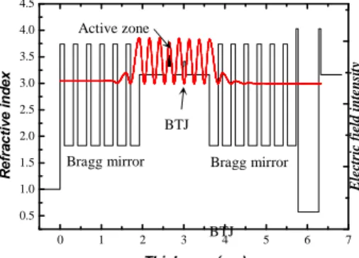
The optical design objectives consist in reaching a high reflectivity of the DBR and optimizing InP thicknesses to place the active zone at an electric field crest and the BTJ at a trough.
Figure 1. Electrically pumped VCSEL structure
Optical simulation algorithm contains two parts: from the optical properties of each layer of the structure (thickness, refractive index, absorption), the algorithm first part, based on propagations matrices, gives access to the electric field, the reflectivity spectrum. The second part characterizes the active zone. It gives access to the QW energy levels, the oscillator strengths to calculate gain, absorption or spontaneous emission spectra. The epilayer structure is then optimized to reach monomode VCSEL properties around λ = 1.55 µm.
The DBRs are realized by magnetron sputtering. The dielectric materials are amorphous silicon (a-Si) and amorphous silicon nitride (a-SiNx). Two ways are envisaged to reach such a reflectivity. A standard DBR is realized using 6 periods and presents a reflectivity value of 99.6% at λ = 1.55 µm. Thanks to a simulation based on propagations matrices using the refractive indexes of each layer, a hybrid DBR with 3 and half periods and gold layer is shown to have the same reflectivity. Such mirrors have been realized and their reflectivity measured by FTIR (Fourier Transform Infrared Reflexion) is in good agreement with simulation results.
The active zone, grown by molecular beam epitaxy (MBE), contains 6 InGaAs 7.2 nm large quantum wells (QW). Lattice matched alloy (In0.8Ga0.2As0.435P0.565 named Q1.18 because its gap
corresponds to λ=1.18 µm) is used as a 10 nm large barrier. The buried tunnel junction is realized in strongly doped (ND = NA =
5.1019 cm-3) lattice matched InGaAsP alloy (Q1.4). This alloy has
been chosen for its small gap to enhance tunneling properties avoiding absorption at λ = 1.55 µm. As shown on Fig. 2, the active zone and BTJ positions are optimized adjusting InP thicknesses. The total reflectivity of the structure presents a free spectral range of 50 nm: a monomode VCSEL is thus expected.
0 1 2 3 4 5 6 7 0.5 1.0 1.5 2.0 2.5 3.0 3.5 4.0 4.5 R e fr a c ti v e i n d e x Thickness (µm) E le ct ri c fi el d i n te n si ty
Figure 2. Electric field repartition in the structure
6QWs InP n+ Q1.18 (30 nm) Q1.18 (30 nm) InP p+ Q1.18 p+ (10 nm) Q1.4 p++(25 nm) Q1.4 n++(25 nm) InP n+ Active zone Bragg mirror Bragg mirror InP n+ Contact BTJ
Bragg mirror Bragg mirror
Active zone
BTJ BTJ
III. THERMAL ANALYSIS 10 20 30 40 50 1.566 1.568 1.570 1.572 1.574 1.576 1.578 1.580 1.582 0.22nm/mW 0.29nm/mW E m is si o n w a ve le n g th ( µ m ) Pump power (mW) conventional mirror hybrid mirror
Figure 3. Wavelenght shift as a function of pump power for VCSELs with conventional or hybrid DBR. Simulation (full line) is in good agreement with
experiment (squares and circles).
0 1 2 3 4 5 6 7 1500 1600 1700 1800 1900 2000 2100 2200 2300 2400 T h er m a l re si st a n ce ( K /W ) InP thickness (µm)
Figure 4. Electrical VCSEL thermal resistance as a function of InP thickness.
Heat dissipation is an important problem in VCSELs due to the small active zone compared to edge lasers [4]. The aim of thermal analysis is to design the metallic contacts and the epilayer structure to enhance thermal conductivity. A 2-dimension (with revolution symmetry) finite element model has been used to model optically and electrically pumped VCSELs. 2 optical structures have been fabricated, using standard and hybrid DBR. Their wavelength shift has been measured as a function of pump power as shown on figure 3. Considering a thermal shift of 0.1 nm/K for 1.55 µm wavelength, the VCSEL thermal resistance is evaluated to 2.9 K/mW for the standard DBR and 2.2 K/mW for the hybrid VCSEL. These values are in good agreement with simulation results. For electrically pumped VCSEL, the InP thickness effect on thermal resistance has been simulated as shown on Fig. 4. For a 200 nm InP thickness, the electrical VCSEL thermal resistance is 2.36 K/mW, almost the same value as for optical hybrid VCSEL.
IV. BURIED TUNNEL JUNCTION
In electrically pumped VCSELs, the BTJ allows carrier and optical confinement in the active zone. To fabricate the VCSEL structure shown in Fig. 1, a first MBE growth is performed until the Q1.4 layer, followed by the Q1.4 mesa chemical etching (a 15
nm InP layer is over-etched to ensure the current confinement). The end of the structure is re-grown by MBE. A self-consistent 1D Schrödinger-Poisson algorithm is used to verify the tunnel effect in the reverse BTJ and to avoid current leakage in the reverse InP junction outside the BTJ. If the depletion region is too large and reaches the laser active zone, electrical injection is no more confined. -6 -5 -4 -3 -2 -1 0 E n e rgy ( e V ) Active Zone Q1.18 153 nm InP p+ 30 nm BTJ InP n InP n InP n VB VB CB CB outside the BTJ
Figure 5. Simulation of the band diagram of the VCSEL in vertical direction, inside and outside the BTJ.
Figure 5 presents the bias voltage band diagrams obtained inside and outside the BTJ. The simulated structure corresponds to Fig. 1 except the active zone where quantum wells are not taken into account. Inside the BTJ, Q1.4 doping level is almost
ND = NA = 5.1019 cm-3, which allows a great tunnel effect
verified experimentally by I(V) characteristics. Simulation has shown that a voltage variation only modifies injection current in the BTJ and keeps the band curvature in the active zone constant.
Outside the BTJ, the InP p+ layer has to be thick enough so that a reverse polarization of the InP diode does not modify the active zone curvature. As the maximum p doping level of InP is NA = 2.1018 cm-3, Schrödinger-Poisson simulations have shown
that the minimum InP p+ thickness is 30 nm. First electrical measurements of the VCSEL cavities (without the DBR) have been performed on two samples with an InP p+ thickness of 15 nm and 240 nm. The first sample presents strong leakage current outside the BTJ while the second one avoids this problem. These first experimental characteristics are consistent with simulation results.
CONCLUSION
To design electrically pumped 1.55 µm VCSELs on InP, three useful steps of simulation have been presented, all consistent with experiment. Optical simulation gives access to the epilayer structure and to the DBR reflectivity. A 2D thermal model gives access to the thermal resistance of the structure and a simple 1D Schrödinger-Poisson calculation allows to understand why the first samples fabricated in the laboratory presented leakage current. An integrated VCSEL model including these three steps of simulation could be useful to improve this VCSEL design provided the results stay consistent with experiment.
REFERENCES
[1] M. B. Tayahi, S. Lanka, J. Wang, J. Catsten, L. Hofmann, and S. Sukanta, “High volume production of single mode VCSEL” Proc. SPIE, 6132, 613202, 2006
[2] A. Karim, S; Björlin, J. Piprek and J.E. Bowers, IEEE J. Sel. Top.
Quantum Electron. 6, 1245, 2000
[3] C. Levallois, A. Le Corre, S. Loualiche, O. Dehaese, H. Folliot, C. Paranthoën, F. Thoumyre, C. Labbé, J. Appl. Phys. 98, 043107, 2005 [4] M. Osinski, W. Nakwaski, IEEE J. Sel. Top. Quantum Electron.1, 681,