HAL Id: pastel-00761566
https://pastel.archives-ouvertes.fr/pastel-00761566
Submitted on 5 Dec 2012HAL is a multi-disciplinary open access archive for the deposit and dissemination of sci-entific research documents, whether they are pub-lished or not. The documents may come from teaching and research institutions in France or
L’archive ouverte pluridisciplinaire HAL, est destinée au dépôt et à la diffusion de documents scientifiques de niveau recherche, publiés ou non, émanant des établissements d’enseignement et de recherche français ou étrangers, des laboratoires
La croissance plasma de nanofils de silicium catalysée
par l’étain et l’indium et applications dans les cellules
solaires à jonctions radiales.
Benedict O’Donnell
To cite this version:
Benedict O’Donnell. La croissance plasma de nanofils de silicium catalysée par l’étain et l’indium et applications dans les cellules solaires à jonctions radiales.. Science des matériaux [cond-mat.mtrl-sci]. Ecole Polytechnique X, 2012. Français. �pastel-00761566�
Benedict O’Donnell
P
L A S M A G R O W N S I L I C O N N A N O W I R E S
CATALYZED BY POST
-
TRANSITION METALS
&
A P P L I C A T I O N S I N R A D I A L J U N C T I O N S O L A R C E L L SThèse
présentée en vue d’obtenir le grade de
Docteur de l’École Polytechnique
Spécialité « Science des Matériaux »
par
B
ENEDICT
O‘D
ONNELL
[email protected]
P
LASMA GROWN SILICON NANOWIRES CATALYZED BY POST
-
TRANSITION METALS
&
APPLICATIONS IN RADIAL JUNCTION SOLAR CELLS
Thèse à soutenir le 3 décembre 2012 devant le jury composé de:
D
R
.
S
ILKE
C
HRISTIANSEN
R
APPORTEUR
D
R
.
J
EAN
-C
HRISTOPHE
H
ARMAND
R
APPORTEUR
D
R
.
A
NTON
Í
N
F
EJFAR
E
XAMINATEUR
P
ROF
A
NNA
F
ONTCUBERTA I
M
ORRAL
E
XAMINATRICE
P
ROF
. T
HIERRY
G
ACOIN
E
XAMINATEUR
D
R
.
V
OLKER
S
CHMIDT
E
XAMINATEUR
D
R
.
M
ARC
V
ERMEERSCH
E
XAMINATEUR
A Carmen Gonzalez Martinez & Pere Roca i Cabarrocas, por darme ollos i ensenyar-me a veure.
Contents
LIST OF TABLES ... III
LIST OF FIGURES ... V
LIST OF ACRONYMS ... VII
1.
INTRODUCTION ... 1
1. Sustainable economics ... 2
2. The physics of photovoltaic energy conversion ... 4
3. PV markets and manufacturing costs ... 10
4. Conducting charges and trapping light in a-Si:H ... 16
5. Conclusion ... 21
2.
ORGANIZING DROPS OF METAL ... 29
1. Nanowire catalysts and surface science ... 30
2. Dewetting layers of evaporated tin ... 32
3. Reducing layers of metal oxides ... 35
4. Thin layers of tin and ITO over stable zinc oxide ... 46
5. Conclusion ... 51
3.
VLS GROWTH CATALYZED BY POST-TRANSITION METALS... 59
1. Nanowires and Vapour-Liquid-Solid growth ... 60
2. Practical considerations in choosing nanowire catalysts ... 62
3. Post-transition metals and plasma enhanced VLS... 67
4. Conclusion ... 75
4.
SN-CATALYZED SINW GROWTH ... 85
1. Sn-catalysts and plasma-assisted VLS fabrication conditions ... 86
2. Parameters influencing the nanowire growth rate ... 88
3. Straight and faceted SiNW growth ... 96
4. Conclusion ... 105
5.
RADIAL JUNCTION SOLAR CELLS ... 111
1. Introducing radial junction photovoltaics ... 112
2. Radial junctions grown at low temperature ... 115
3. Radial junctions grown at high temperature ... 125
4. Light trapping in radial junctions ... 131
5. Conclusion ... 138
CONCLUSION ... 145
APPENDIX: MEASURED AND NOMINAL TEMPERATURE ... 147
LIST OF PUBLICATIONS ... 149
ACKNOWLEDGEMENTS ... 151
List of Tables
Table 2.1: Plasma conditions for reducing SnO2 & ITO layers ... 36
Table 2.2: Plasma conditions for coating the Plasfil chamber with a-Si:H ... 41
Table 2.3: Metal drops formed from metal films of different thickness ... 52
Table 2.4: Metal drops formed under longer or higher power H2 plasmas ... 52
Table 2.5: Metal drops formed from TCOs reduced by H2 plasma under different temperatures ... 53
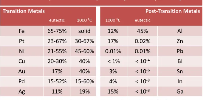
Table 3.1: Equilibrium solubility of Si in liquid metals ... 68
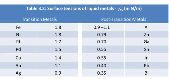
Table 3.2: Surface tension of liquid metals ... 70
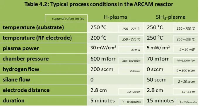
Table 4.1: Typical process conditions in the Plasfil reactor ... 87
Table 4.2: Typical process conditions in the ARCAM reactor ... 88
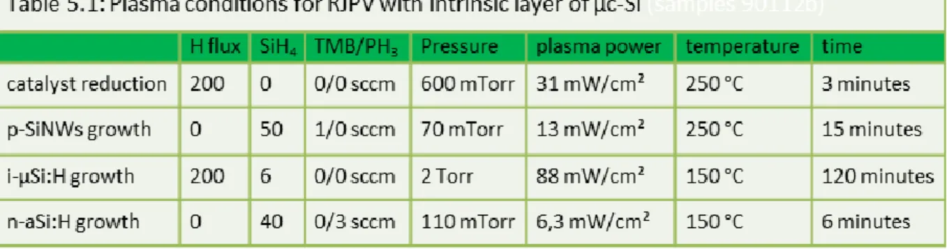
Table 5.1: Plasma conditions for RJPV with µc-Si:H absorbers ... 117
Table 5.2: Plasma conditions for removing SiNWs in a H2 plasma ... 118
Table 5.3: Plasma conditions for RJPV using an a-Si:H absorber ... 119
Table 5.4: ITO window layer sputtering conditions for superstrate RJPV. ... 121
Table 5.5: Plasma conditions for RJPV with different diameters and densities ... 123
Table 5.6: Plasma conditions for RJPV fabricated on straight SiNWs grown at 600 °C ... 126
Table 5.7: RJPV with different TMB concentrations ... 128
Table 5.8: Plasma conditions for RJPV with different lengths ... 131
List of Figures
1.1 - Global energy resources. ... 4
1.2 - The energetic decay of excited electrons. ... 6
1.3 - Schematic representation of the band diagram within the PN junction. ... 7
1.4 - The electronics of a solar cell. ... 8
1.5 - Increasing PV capacity and decreasing Feed-in Tariffs. ... 11
1.6 - Silicon PV manufacturing steps. ... 13
1.7 - Break-down of manufacturing cost per WP of polycrystalline silicon photovoltaic modules. ... 14
1.8 - Break-down of manufacturing costs per WP of thin-film silicon photovoltaic modules. ... 15
1.9 - Comparing the total cost of polycrystalline and thin-film silicon PV system installations. ... 15
1.10 - Atomic configuration and density of states in a-Si. ... 17
1.11 - Conventional light trapping in an a-Si:H solar cell. ... 19
1.12 - Light trapping in a radial junction solar cell. ... 20
2.1 - Tensile forces acting on a liquid drop. ... 31
2.2 - Metal drop formations for thicker layers of Sn. ... 32
2.3 - Diameters of drops formed by increasingly thick layers of Sn. ... 33
2.4 - Diameters of Sn drops formed on glass and crystalline Si substrates... 33
2.5 - Effect of H2 plasma at 250 °C on the formation of Sn drops. ... 34
2.6 - Effect of plasma power and duration on Sn drop formation. ... 34
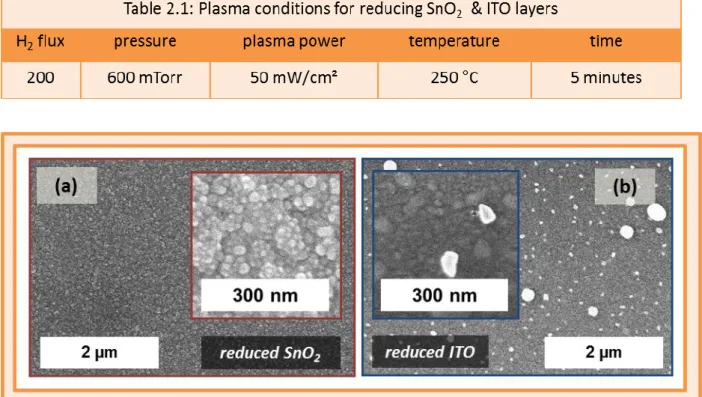
2.7 - SnO2 and ITO substrates exposed to a H2 plasma. ... 36
2.8 - Diameter of Sn drops reduced from SnO2 substrates in a H2 plasma. ... 37
2.9 - Diameter of metal drops reduced from ITO substrates in a H2 plasma. ... 38
2.10 - Metal drops reduced from ITO substrates during increasingly long H2 plasma exposures. ... 38
2.11 - Volume of metal reduced at the surface of SnO2 and ITO layers in a H2 plasma. ... 39
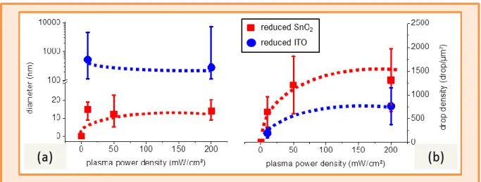
2.12 – Diameter and density of metal drops reduced from SnO2 and ITO layers in a H2 plasma. ... 39
2.13 - Effect of H2 plasma power density on the reduction of SnO2 and ITO. ... 40
2.14 – Effect of H2 plasma power on metal drops reduced from SnO2 and ITO layers. ... 41
2.15 - Contamination from sidewall Si deposition. ... 42
2.16 - Effect of H2 plasma temperature on metal drops reduced from SnO2 and ITO layers. ... 43
2.17 – Diameter and density of metal drops reduced from ITO and SnO2 layers as a function of temperature. . 44
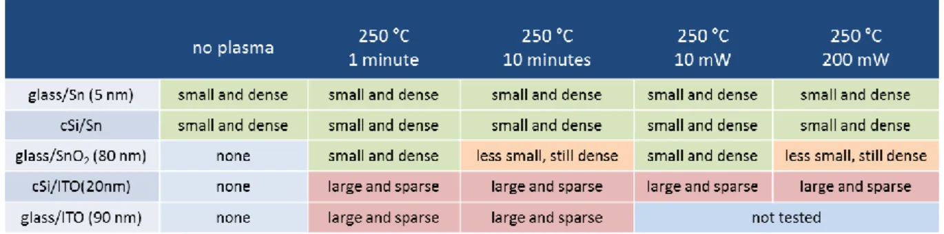
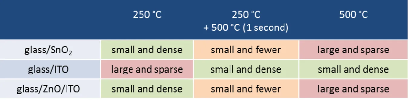
2.18 - Step-by-step response of glass/SnO2 substrates to heating and plasma reduction. ... 44
2.19 - Step-by-step response of cSi/ITO substrates to heating and plasma reduction. ... 45
2.20 - Step-by-step response of ZnO/ITO substrates to heating and plasma reduction. ... 46
2.21 - Metal drops reduced from increasingly thick ITO layers. ... 47
2.22 - Diameter and density of metal drops reduced from increasingly thick layers of ITO. ... 47
2.23 - Effect of reduction temperature on thin (1 nm) layers of ITO. ... 48
2.24 - Effect of temperature on metal drops reduced from layers of ITO. ... 49
2.25 - Surface features of ITO layers reduced in a H2 plasma. ... 49
2.26 - Sn drops formed on ZnO with increasingly thick layers and high reduction temperatures... 50
2.27 - Observations of nanowire growth on glass/ZnO substrates covered in wetting Sn. ... 51
2.28 - Lower density metal drops reduced from layers of ITO in lower temperature H2 plasmas. ... 54
3.1 - The VLS growth mechanism. ... 60
3.2 - Equilibrium solubility and degradation thresholds for various metals in silicon. ... 63
3.3 - Ionization energies and degradation thresholds of different metals in crystalline silicon. ... 64
3.4 - Summary of abundances, eutectic points and ionization energies in Si for potential SiNW catalysts. ... 66
3.6 – Surface tension equilibrium during SiNW growth. ... 70
3.7 - The risk of oxidation when growing Sn-catalyzed SiNWs. ... 72
3.8 - SiNWs grown using Sn, In and Bi catalysts. ... 73
3.9 – The distinction between transition and post-transition metals as SiNW catalysts. ... 74
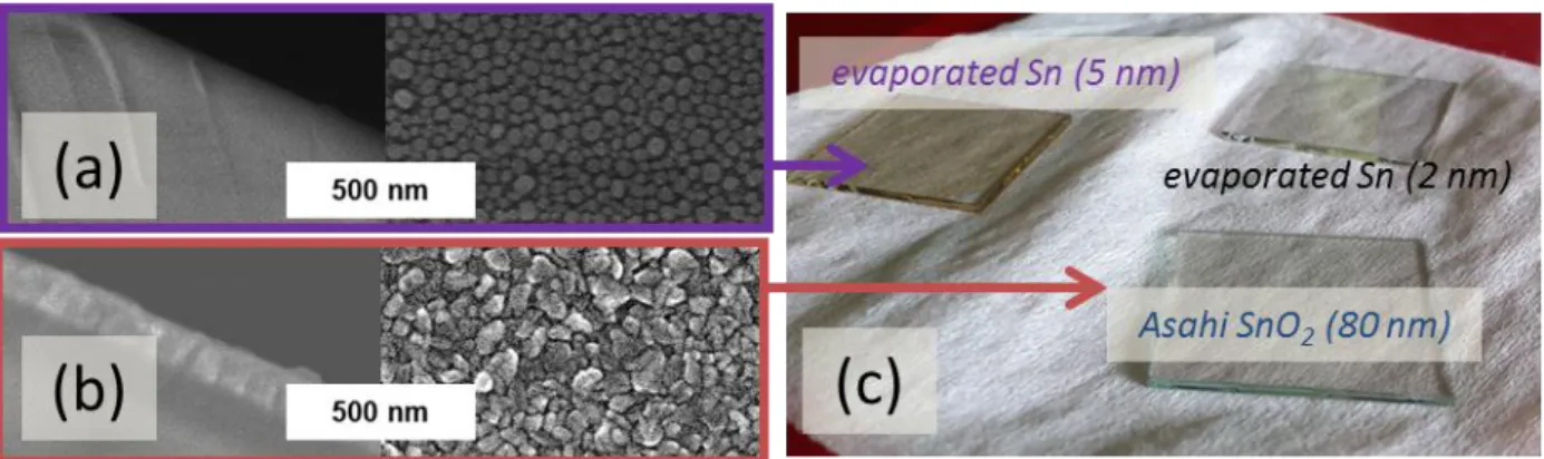
4.1 -- Arcam and Plasfil PECVD reactors. ... 86
4.2 - Substrates used in the SiNW morphology optimization studies. ... 87
4.3 - Sn-catalyzed SiNW length as a function of growth time. ... 89
4.4 - Diameter of Sn-catalyzed SiNW grown in the ARCAM reactor. ... 90
4.5 - Catalyst drops not found at the tip of Sn-catalyzed SiNWs grown at 600 °C. ... 90
4.6 - Density of Sn-cataylzed SiNWs and catalyst drops. ... 91
4.7 - Incubation period of Sn-catalyzed SiNWs grown in Plasfil. ... 92
4.8 - Effect of silane pressure on the growth of Sn-catalyzed SiNWs. ... 93
4.9 - Effect of hydrogen concentration on the growth rate of Sn-catalyzed SiNWs. ... 94
4.10 - Dimensions of Sn-catalyzed SiNWs grown under different H2 concentrations. ... 94
4.11 - Effect of plasma power on the growth rate of Sn-catalyzed SiNWs. ... 95
4.12 - Effect of temperature on the crystallinity of Sn-catalyzed SiNWs. ... 97
4.13 - Effect of temperature on the crystallinity of SiNWs grown with different catalysts. ... 97
4.14 - Effect of high temperature on the growth rate of Sn and In-catalyzed SiNWs. ... 98
4.15 - Absence of catalysts at the tip of In-catalyzed SiNWs grown at high temperature. ... 99
4.16 - Faceting over the sidewalls of In-catalyzed SiNWs grown at temperatures higher than 600 °C. ... 99
4.17 - Faceting over the sidewalls of Sn-catalyzed SiNWs grown at temperatures higher than 600 °C. ... 100
4.18 - Faceting on SiNWs of various diameters grown from catalyst which diffused about a localized Sn pad. 101 4.19 - Range of diameters of metal drops and SiNWs produced by a localized Sn pad. ... 101
4.20 - Faceting on Sn-catalyzed SiNWs grown over a temperature gradient. ... 102
4.21 - Transition from faceted to cylindrical growth in Sn-catalyzed SiNWs. ... 103
4.22 – Limiting diameters for faceting in Sn-catalyzed SiNWs. ... 104
5.1 – Sn-catalyzed SiNWs and radial PIN junction solar cell grown by PECVD. ... 112
5.2 - Fabrication steps for our first radial junction devices. ... 116
5.3 - Radial junction solar cells with µc-Si:H absorbers. ... 117
5.4 - Sn-catalyzed SiNWs exposed to a H2 plasma. ... 118
5.5 - Radial junction solar cells with a-Si:H absorbers... 119
5.6 – Radial junction solar cells in substrate and superstrate configurations... 120
5.7 - SR and J(V) characteristics of substrate and superstrate solar cell configurations. ... 121
5.8 - Substrates used for radial junction array density studies. ... 122
5.9 - Density of SiNW arrays according to different substrates. ... 123
5.10 - Optical absorptance of radial junction solar cells with different array densities. ... 124
5.11 - J(V) characteristics of radial junction solar cells with different array densities. ... 125
5.12 - Radial junction solar cells on intrinsic SiNWs grown at high temperature. ... 126
5.13 - Radial junction solar cells on p-type SiNWs grown. ... 127
5.14 - Radial junction solar cells with increasing TMB concentration during SiNWs growth. ... 128
5.15 - Conformal coverage of layers over Sn-catalyzed SiNWs deposited at 600 °C. ... 128
5.16 - Conformal coverage of ITO contacts on radial PIN junctions. ... 129
5.17 - J(V) characteristics of radial junction, planar and conventionally textured solar cells. ... 130
5.18 - Optical absorptance of radial junction solar cells grown on increasingly long SiNWs. ... 132
5.19 - J(V) characteristics of radial junction solar cells grown on increasingly long SiNWs. ... 133
5.20 – Optical losses at low wavelengths in our radial junction solar cells. ... 134
5.21 - Radial junction solar cells with increasingly thick ITO layers. ... 135
List of Acronyms
Units a-Si:H Hydrogenated amorphous silicon
c-Si Crystalline Silicon
CVD Chemical Vapor Deposition
FF Fill factor %
ITO Indium-Tin-Oxide
JSC Short-circuit current density mA.cm-²
PA-VLS Plasma Assisted Vapor-Liquid-Solid
PECVD Plasma Enhanced Chemical Vapor Deposition
PV Photovoltaic
RS Series resistance .cm²
RSH Shunt resistance .cm²
sccm Standard Cubic Centimeters per Minute
SEM Scanning Electron Microscopy
SiNW Silicon Nanowire
UHV Ultra-Hugh Vacuum (pressures < 10-6 mbar)
VLS Vapor-Liquid-Solid
VOC Open circuit voltage mV
Chapter 1: Introduction
Quote from Lady Windermere's Fan, Oscar Wilde, 1892.
1. Introduction
1.
SUSTAINABLE ECONOMICS ... 2
1.1. Volatile fuels ... 2
1.2. Unknown reserves... 3
1.3. The solar resource ... 3
2.
THE PHYSICS OF PHOTOVOLTAIC ENERGY CONVERSION ... 4
2.1. The equivalent circuit representation of the photovoltaic cell ... 7
2.2. How to read a current-voltage characteristic ... 8
2.3. What is a Watt peak? ... 9
3.
PV MARKETS AND MANUFACTURING COSTS ... 10
3.1. A history of photovoltaics ... 10
3.2. The photovoltaics sector in the 2010s ... 11
3.1. Breaking down the manufacturing costs of crystalline silicon PV ... 12
3.2. Short-cuts and hydrogenated amorphous silicon ... 14
4.
CONDUCTING CHARGES AND TRAPPING LIGHT IN A-SI:H ... 16
4.1. Light trapping and texturing ... 18
4.2. Silicon nanowires and the radial junction solar cell ... 20
5.
CONCLUSION ... 21
“We are all in the gutter, but some of us are looking at the stars.”
The frenetic activity of mankind is fed predominantly by fuels which are finite, located in politically sensitive areas and emit gases that destabilize the Earth climate. As the human species grows more numerous and wealthier, consumption of these risk-prone resources is set to accelerate. In this chapter, we explore the potential of photovoltaic solar energy conversion to meet future demands sustainably. The history of the technology is outlined to highlight the developments which have permitted its recent expansion. The most common industrial practices involved in their fabrication process are also described, in order to draw attention to some of the difficulties in lowering their cost and identifying how radial junction solar cells can contribute to the widespread adoption of photovoltaics.
Chapter 1: Introduction
1. Sustainable economics
When averaged over 2010, human activity consumed energy resources at the staggering rate of 16 TW.1 There are few forces in nature which compare to this figure. It surpassed the annual power output of lightning bolts (0.01 TW),2, 3 earthquakes (0.4 TW),4 waves (3 TW)5 and tides (3.7 TW).6 Considering that the payload of the 1945 Fatman nuclear bomb unleashed 1014 J,7 its scale may be glimpsed by considering that, each day, mankind employs enough energy to destroy every city of over 500 000 inhabitants it has ever built.8 Although daunting, this ravenous appetite for energy reflects highly desirable increases in food production, housing construction, travel, living standards... The grave threat shackled to our current energy consumption does not lie in its scale, but in its source.
1.1. Volatile fuels
Since the industrial revolution, human development has been powered predominantly by burning fossil fuels. These fuels are the remains of living organisms buried over millions of years in the planet crust. While alive, they stored energy from the Sun in chemical bonds which have gradually decayed into forms which include coal, natural gas and oil. These fuels present several advantages over living vegetation. Their energy density is generally higher, making it possible to store more Joules in a lighter load.9 Their production occupies little agricultural land. Their liquid or gaseous form can make them easier to handle. And they are substantially cheaper to “produce” than any crop.10 These advantages have historically outweighed some of their less flattering attributes. Reserves of fossil fuels are locally concentrated, leading to political tension between exporter and consumer countries (characteristically between the West and the Middle East or Eastern Europe and Russia) or over territorial ownership (as in the case of Darfur or the South China Sea).11 Their extraction and combustion lead to health hazards,12 acid rains,13 ground contamination,14 water contamination15 and are beginning to disrupt the world climate.16 In addition to these concerns, there is also the unsettling threat of their depletion.
Box 1: Fossil fuels and greenhouse gases.
The combustion of fossil fuels releases greenhouse gases (notably CO2, CH4 and N2O) which build up in the atmosphere and raise the average temperature of the planet by reflecting heat leaving its surface. Since the industrial revolution, the atmospheric concentration of these gases has soar to values unprecedented in over half a billion years.17, 18 Global temperatures have risen by 0.5 °C and are expected to increase by several degrees Celsius within the next five decades.19 These figures verge on the difference between current temperatures and those of the last ice age.20 Such rapid changes to the Earth climate threaten its biosphere with massive extinction.21, 22 They are already affecting weather patterns and drying agricultural land in regions prone to food shortages.23 They are intensifying extreme meteorological events such as tornadoes and they are causing mountain glaciers19 and ice sheets to melt, raising flood risks across entire countries.23 The complexity of the climate system leaves many disturbing questions unanswered. However the effects mentioned are
Chapter 1: Introduction
all set to worsen as more fossil fuels are burnt and the concentration of greenhouse gases increases in the atmosphere.
1.2. Unknown reserves
The amount of oil, gas and coal which remains to be recovered from the ground is unknown. The International Energy Agency estimates that, at current consumption rates, proven reserves (fuel deposits with a 90% chance of being profitably extracted, depending on future prices and technology) can supply the world with oil for the coming 40 years, gas for 60 years and coal for 200 years.24 Optimistic estimates with regards to progress in exploration, extraction techniques and energy prices could possibly boost these figures by a factor of 3 for oil, 4 for gas24 and 20 for coal.25 However, current consumption rates are far from static. The world population is growing fast and two thirds of it resides in rapidly developing economies in which patterns of energy consumption are booming from Third World to Western standards. Over the past three decades, oil, coal and natural gas consumption rates have increased by 30%, 90% and 100% respectively and energy demand will continue to increase in the decades to come.24
There are also considerable uncertainties regarding calculations of recoverable reserves. Although coal is plentiful, only a fraction of it has the energy content expected from the variants used today. There is little evidence as to how much of the rest will ever be energetically favorable to mine, and official sources have recently downgraded their estimates of useable reserves by as much as 90%.26, 27
Several disconcerting observations imply that global oil production may already have reached a tipping point. Despite massive investment in exploration, the size and number of newly discovered oil fields has dwindled over the past decades.24, 28 Stubbornly high energy prices since the turn of the millennium suggest that incremental advances (e.g. offshore drilling or hydraulic fracturing) are hard pressed to follow even current demand trends.29-31 Recent industry figures also indicate that the imbalance in the market is growing, with increases in global oil production lagging behind increases in consumption in 7 of the past 10 years.1
As the supply of fossil fuels contracts, their prices will rise, bringing fuels from previously unprofitable sources to the market. However, these substitutes will not prevent recession in sectors relying on cheap fuel. Such a shift from increasing to decreasing energy supplies is unprecedented in human history and bodes ill for economies which function on the prospect of sustained growth.32
1.3. The solar resource
The words of Oscar Wilde retain wisdom through the ages. How perverse to scavenge for toxic fossils in the bowels of the lithosphere, when the answer to the problem shines right above our heads. The Earth orbits a nuclear reactor which continuously radiates 90’000 TW of clean and ubiquitous power to its surface.33 This input raises storms, runs rivers and breathes life into an otherwise desolate rock. It dwarfs the already-colossal rate of human energy consumption thousands of times over. In fact each year the land and oceans absorb close to 3000 ZJ from the Sun. This is dozens of times larger than the proven reserves of all fossil fuels combined, and even several times their total resource base (Figure 1.1). This vast amount of energy is not cheap; it is free. However the machines that convert it
Chapter 1: Introduction
into the kind of energy we can use are currently expensive. One of the greatest challenges of our time is to find an economical way of harnessing it.
1.1 - Global energy resources.
Geometric representation comparing the scale of remaining energy resources.24, 25, 33, 34 The resource base includes all deposits geologically expected (but not necessarily discovered) and proven reserves are known deposits with a 90% chance of being profitably extracted. (1 zetajoule (ZJ) = 1021 J)
2. The physics of photovoltaic energy conversion
One way of tapping into the vast resource of solar energy is to convert it into electricity using photovoltaic cells. To understand the conversion process, let us define the nature of the energy we are harnessing, and what it is that we want to transform it into. Electricity manifests the redistribution of electrons as they minimize their potential energy. Photons, the elementary particles which compose light, can easily be converted into the potential energy of electrons by exposing them to an opaque material. When they interact, the electrons in the material can absorb the photons which excite them to higher energy states. However, the energy is generally lost within picoseconds to heat in the material. This process is illustrated in Figure 1.2.a, in which the electron cascades back to a state with lower potential energy by conferring the energy gained from the photon to phonons (i.e. vibrations in the atomic lattice). A photovoltaic cell must fulfill two essential conditions to convert the potential energy of its electrons into electricity. The first is to trap the electrons in states which will not decay for as long as it takes to harness their energy. The second is to transform this energy into a form which can be used.
Both these conditions can be met quite elegantly using semiconductors. Semiconductors are a category of materials which conduct electricity only when stimulated to do so (e.g. Si, Ge, GaAs,…). Their main characteristic is that the distribution of energy levels occupied by their electrons is interrupted by what is commonly referred to as a bandgap. At equilibrium, the highest energy state
Chapter 1: Introduction
Box 2: Alternatives
Our comparison has so far neglected the potential of other energy sources to contribute to the global energy mix. The following is a brief overview of the relative merits of biomass, nuclear, wind, geothermal, wave and tidal energy. The interested reader is referred to MacKay35 or Tester et al.5 for further information.
Biomass (in the form of wood, sugar cane, agricultural waste…) remains the fourth most widespread fuel used on Earth. In 2010, it provided 0.05 ZJ of potentially carbon neutral energy. In principle, biomass is free from the environmental and depletion constraints of fossil fuels and work is going into increasing its yield and profitability.36 In practice, large-scale adoption entails a risk of competing with food production for agricultural land (another commodity in short supply).
Nuclear fission is currently the most established and profitable alternative. However in its current form, it is also plagued with concerns regarding uranium fuel supplies.37, 38 Given adequate funding for development, breeder reactors could foreseeably overcome this obstacle. However, the technology would still suffer from issues of nuclear safety, proliferation and waste which, with each passing generation, seem less likely to be solved.39 Nuclear fusion is a commendable pursuit. But it remains too far removed in the future to deal with any imminent risks of fossil fuels.40
The share of wind energy has increased rapidly over the past two decades and grew to account for 0.2 TW of global power capacity in 2010.41 In certain regions, its price has even converged with that of nuclear and coal generated electricity.42, 43 There remains considerable uncertainty on the amount of power which could ultimately be recovered from the wind; however several academic estimates have placed the upper limit at dozens of terawatts.44, 45
Geothermal energy generation consists of extracting heat in the ground which originates predominantly from radioactive decay in the Earth crust. It is extracted by injecting water down boreholes and collecting heat or steam. Depending on the depth at which one drills, 10 – 50 mW/m² can be harnessed virtually anywhere on the planet. At tectonic fault lines (notably in Iceland, the Philippines…) geothermal energy is already a profitable business which contributed 0.01 TW to the global energy mix in 2010.46 However if used sustainably on a large scale, it would be hard pressed to contribute more than 2.6 TW to the global power output.35 Energy from the motion of water flows has been harnessed for millennia. Hydroelectric dams currently contribute 0.4 TW to the global energy mix,24 a handful of tidal dams add another 0.05 TW and the first prototypes for wave energy systems are being tested. However, the technical potential for hydropower is estimated at 1.9 TW 47 and the power driving global marine flows represents 6.7 TW,5, 6 (of which only a fraction can possibly be harnessed). While substantial, the scale of hydrological resources is insufficient to cater for global energy demand.
Chapter 1: Introduction
bind the material together). Because there are no energy levels directly above the valence band, photons with less energy than the bandgap cannot be absorbed by electrons in the material. Instead they shine through it as is demonstrated by glass and water which appear transparent because their bandgap exceeds the energy of visible light. In contrast, photons with energy greater than the bandgap can excite valence band electrons to a second continuum of energy states above the bandgap. Because electrons in these higher energy states can conduct electricity, the continuum of states is referred to as the conduction band. The energy barrier provided by the bandgap is of particular interest in photovoltaics because, to a limited extent, it works both ways. When excited electrons reach the lowest energy state in the conduction band, the bandgap makes low-energy phonon decay impossible (Figure 1.2.b) and the electrons remain excited until they release the energy in the form of a photon. In an indirect bandgap semiconductor such as silicon, this can take up to milliseconds. The timescale is long enough to carry the charges across the semiconductor to external contacts where the energy that they have gained from photons can be harvested.
1.2 - The energetic decay of excited electrons.
Schematic representation of electronic de-excitation in metals (a) and semiconductors (b).
The second condition can be met by using a PN junction to convert the excited electrons into a source of voltage. A PN junction is a semiconductor in which one extremity has been doped p-type and the other n-type. Doping is a process whereby atoms with a different number of valence electrons are incorporated into the semiconductor matrix. For instance, silicon can be doped n-type by adding phosphorous atoms to it. Because phosphorous has a valence of 5, one electron in each phosphorous atom will be unable to bond in the tetravalent Si crystal and will be free to diffuse through the semiconductor. Phosphorous is therefore known as an electron donor in silicon. If instead the dopant is boron, which has a valence of 3, an electron vacancy will be created in the silicon matrix (which can be represented as a positively charged quasiparticle known as a hole). Hence, boron is an electron acceptor in Si. Electrons and holes will diffuse across the interface between the p and n-type regions and recombine, depleting the region surrounding their interface of free charges. In doing so, the ions in the depletion region will remain locked in the crystal matrix,
Chapter 1: Introduction
of sunlight to the conduction band, they are subject to the field and drift towards the n-type region of the PN junction. Likewise, the holes they leave in the valence band drift towards the p-type region. Charges will continue to accumulate in this way until the electric field which they generate compensates the built-in field of the PN junction. The accumulation of charges can be used as a voltage source. By connecting the two extremities of the cell, electrons accumulated in the n-type region can circulate to the p-type region through an external circuit in the form of an electric current. It is useful to describe this process in terms of the band diagram of the device. The tendency of a semiconductor to incorporate or surrender electrons is expressed by the energy separating its conduction band from its Fermi level. When bringing p- and n-type doped semiconductors together, electrons flow from the n-doped region to the p-doped region (and vice-versa for holes) until the density of charge carriers reaches thermodynamic equilibrium. This aligns the Fermi levels between the two materials and establishes a gradient in the energy of the conduction and valence bands across the depletion region (Figure 1.3), preventing further electron diffusion from n-type to the p-type material. It is this gradient in the energy of the band states which causes the photovoltaic effect.
1.3 - Schematic representation of the band diagram within the PN junction.
When a photo-excited electron diffuses within the space charge region, it minimizes its potential energy by drifting to the n-type region (and vice-versa for holes). As more charges are excited and accumulate in either region of the cell, they bend the conduction and valence bands against the initial gradient of the PN junction. The accumulation of charges saturates when the bands are realigned to the extent that there is no longer an energetic gain for newly photo-excited electrons and holes to drift to separate extremities of the cell.
2.1. The equivalent circuit representation of the photovoltaic cell
There is a subtlety involved in extracting the energy from photogenerated electrons efficiently. To grasp this point, it is useful to represent the solar cell as a series of basic electronic components as
Chapter 1: Introduction
illustrated in Figure 1.4.a. The charges built up at the extremities of the cell can produce a current in an external circuit. This aspect of the PV cell is therefore modeled as a current source in the equivalent circuit. Resistive losses can be expected within the cell (arising from charge transport within materials and at the interfaces between different layers). These losses are summed up as a resistor placed in series with the current source. The PN junction also drives electrons towards the n-type layer, but prevents them from approaching the p-n-type layer. A diode placed in parallel with the external circuit represents this asymmetric behavior with respect to the direction of current flow. Last, the PN junction is not a perfect diode and charges can leak through it. There is therefore another path through which electrons can reach the p-layer, which is referred as the shunt path. It is represented by a resistor, also in parallel to the external circuit. Its resistance represents the quality of the junction (the higher the resistance, the fewer charges leak through the PN junction).
1.4 - The electronics of a solar cell.
Equivalent electric circuit (a) and J(V) characteristics of a photovoltaic cell (b).
As a general rule, the power output of a current source with a fixed voltage is maximized when connected to a lighter load. However, for very small resistances in the external electric circuit, resistive losses (RS) within the material and contacts of the cell will account for a larger share of the voltage drop and reduce the external power output. For large loads, as the voltage drop across the external circuit reaches values close to the break-down voltage of the diode, current leaks through the parallel loop rather than the external circuit in Figure 1.4.a. The optimum is a compromise between a load not too light to be overshadowed by resistive losses, but not too large to induce reverse currents through the junction.
2.2. How to read a current-voltage characteristic
To determine the optimum voltage and test the performance of a solar cell, J(V) (current-voltage) measurements are carried out. In this experiment, the temperature is maintained at 25 °C while
Chapter 1: Introduction
atmosphere when the sun is at a zenith angle of 48.2°. These standardized conditions are referred to as air mass 1.5 (AM1.5) and correspond to a radiative power input of 100 mW/cm² (with the same wavelength distribution as the solar spectrum). The p-type and n-type layers of the cell are connected to both a voltage source and current meter which apply a range of voltages to the cell to replicate the effect of loads with increasing resistivity and measure the current produced by the cell for each.
The current generated by the cell when no voltage is applied s referred to as its short-circuit current (Isc). The applied voltage at which the detected current is zero corresponds to the open circuit voltage (Voc) of the cell. The voltage at which the maximum current x voltage product is recorded is known as Vmax and corresponds to the optimal load for which the solar cell can deliver its maximal power output (the current at this point is known as Imax). The energy conversion efficiency can be determined by dividing Imax x Vmax by the power of incident radiation.The values of Isc and Voc are related to Imax x Vmax by a property known as the fill factor (FF) which can be deduced from the ratio of the product of Imax x Vmax over Isc x Voc. It is often more practical to normalize the current over the area of the cell which is tested and refer to the current density (J) in mA/cm² rather than the absolute current (I) in A.
The objective in optimizing solar cells is to achieve the highest possible energy conversion efficiency
. However, it is insightful to compare the values of VOC, Jsc and FF as these parameters offer information on what is contributing to (or diminishing) the performance of the cell. The open-circuit voltage is determined by the maximum density of charge carriers which can be separated by the PN junction. This depends largely on the bandgap of the material in the depletion region but also on a variety of other factors including the presence of recombination centers in the doped layers of the cell. The short-circuit current of the cell quantifies the rate at which it generates new charge carriers. It is notably correlated to the intensity of incident radiation and therefore limited by optical losses in the device. The fill factor primarily represents recombination across the PN junction and resistive losses within the materials of the cell (modeled in the equivalent circuit of Figure 1.4.a by two resistors, respectively in parallel and in series to the voltage source). The parameters are related to each other, and many common problems (contamination, defaults, excessive doping…) are liable to affect several of them at same time.
2.3. What is a Watt peak?
A Watt peak (Wp) is the unit adopted by the solar industry to quantify the maximal power output of a solar panel (its capacity) under AM1.5 testing conditions. The unit is not normalized with respect to the area of the solar panel (which needs to be taken into account to assess its energy conversion efficiency). Watts peak are rarely quoted in scientific research. However they are useful when calculating the total energy that a solar installation will produce over its lifetime, or the ultimate contribution of installed photovoltaic capacity to the global energy mix. The conditions under which photovoltaic cells operate outside the laboratory rarely coincide with AM1.5 norms. Practical considerations including night time, cloud cover and the angle of inclination of the sun typically lead to averaged annual power outputs of 20% the capacity of the solar panel.48, 49 This fraction is known
Chapter 1: Introduction
as the capacity factor. It applies with different degrees to all energy technologies, as nuclear reactors and fossil fuel plants do not always operate at full capacity either. In the case of photovoltaics, the capacity factor also depends on the region in which the panel is installed, as solar insolation varies across the globe.
3. PV markets and manufacturing costs
In addition to large-scale arguments relating to the future of the world energy supply, there is an immediate business incentive to developing photovoltaics: annual fuel exports are worth $2.3 trillion.50 Generating power is by far the vastest industrial endeavor ever to have occupied mankind. Seven out of the ten largest public companies in the world deal in fossil fuels51 (and are modest players in comparison with the state owned titans not listed on the stock exchange). Global exports in this sector tower over those in financial services ($0.27 trillion),50 agriculture ($1.4 trillion)50 and defense spending ($1.5 trillion).52 Given the scale of the market, even marginal profits in novel energy technologies could reap gigantic rewards. In this section, we assess the obstacles blocking the path of current PV manufacturing to these rewards. Paradoxically, some of the most promising paths to overcoming them can be found by looking, not at the encouraging predictions for future photovoltaic growth,53 but at the meanders of its past. A brief history of photovoltaics is therefore presented before describing the present status of the field and identifying how the following chapters of this thesis may contribute to its development.
3.1. A history of photovoltaics
The prospect of harnessing the energy of the Sun emerged at the tail end of the Enlightenment, when Alexandre Becquerel reported to the French Academy of Sciences that compounds of noble metals immersed in acid could generate a voltage when exposed to light.54 By the 1880s, scientists in the UK and America had shown that a solid state version of the device could also work using metal coated with selenium.55, 56 Interest in these photovoltaic systems remained largely scientific until the 1940s, when researchers at Bell Laboratories steered the field towards solidified silicon melts.57 These highly pure and ordered semiconductors were being developed for the nascent field of microelectronics. They brought energy conversion efficiencies up to an unprecedented 6 percent.58 However, due to their initial fabrication costs, applications remained limited to markets with exceptionally high energy prices. Fortunately, a niche market soon emerged with the advent of the aerospace industry. As of the 1960s, private companies, including Bell Laboratories, Texas Instruments and Sharp, were turning profits from powering satellites with crystalline silicon solar cells.
The oil crises of the 1970s radically changed the landscape of photovoltaics. Concerns in the West about the security of energy imports led to increased funding in renewable energy. Whereas research had previously focused on boosting the conversion efficiency of solar cells, it shifted to bringing down costs for utility-scale applications. Microscopically thin layers of a-Si:H59, CdTe,60, 61 CIGS62 and GaAs63 were developed as potentially economical alternatives to wafers of crystalline silicon. However cheaper materials invariably suffered from lower energy conversion efficiencies,
Chapter 1: Introduction
leading to overall electricity prices which remained higher than those of conventional power plants. By the 1980s, the price of oil had crashed and the price of photovoltaics had not. Although scientific advances continued throughout the following two decades, most notably in areas which interface with organic semiconductors64 and quantum physics65, government and industrial attention waned and solar cells remained largely confined to niche markets.
3.2. The photovoltaics sector in the 2010s
Since the turn of the millennium, the escalation of fuel prices and a growing perception of the risks of climate change23, 66 have revived enthusiasm for sustainable energy and led to the development of a booming photovoltaics industry (Figure 1.5.a). This sudden change of events results mainly from political commitment,67, 68 notably from the introduction of feed-in-tariffs.69 Feed-in-tariffs are laws which force utilities to buy back renewable energy at a price fixed by the government to allow its producers to recuperate the cost of their installation over its lifetime. The price of solar panels is therefore shared among all utility consumers through their electricity bills. This market distortion was designed to encourage investment and R&D in new energy technologies and reduce their manufacturing costs until they grow competitive.
1.5 - Increasing PV capacity and decreasing Feed-in Tariffs.
Cumulative capacity of global photovoltaic installations (a) and the feed-in-tariffs for residential PV systems and electricity prices (€/kWh) in Germany (b) over the past decade.
In many respects, the approach has been remarkably successful. Substantial private funds have been channeled into developing the technology, with demand for solar photovoltaic capacity growing on average by 40% each year over the past decade (Figure 1.5.a).53 When including system components and installations, the PV market has expanded from $2.5 to 71.2 billion over this period.70 As a bonus, it has added 70 GW of peak power capacity to the grid 53 and relieved the atmosphere from tens of megatons ofCO2.24, 53 Outstanding progress has been made towards reducing PV manufacturing costs, as the price of modules has halved with each 10-fold increase in global shipments. 71-73 Trends in electricity prices and feed-in-tariffs indicate that photovoltaics will become competitive in many European markets within the coming decade if the sector can sustain current rates of cost reductions
Chapter 1: Introduction
(Figure 1.5.b). However, with learning curves for established solar technologies saturating and margins across the industry at an all-time low, driving costs down further is likely to require technological innovation. In order to identify where this innovation is most needed, we present a brief overview of current PV manufacturing.
Box 3: The objective and cost of Feed-in-Tariffs.
Germany offers an insightful case study for the global potential of photovoltaics. Because it accounts for the lion’s share of global PV installations, political decisions there (i.e. the feed-in-tariffs it sets) have considerable influence on the entire photovoltaic sector. Its utility prices are not particularly high (as in most of the EU, they have remained between €0.10/kWh and €0.15/kWh since 2003) and its annual insolation is modest compared to most inhabited locations around the world. Nonetheless, the price at which its utilities are legally bound to buy solar generated electricity from residential installations has decreased over the past decade from €0.60 to €0.30/kWh without slowing the rate at which PV capacity is being installed within its borders (Figure 1.5). If these trends are sustained, solar energy could drop below German grid prices within the coming decade. Once they do, market forces will massively increase the installed capacity of photovoltaics and bring on a new paradigm in global energy generation. Risks of fuel depletion and climate change will be averted, and further cost-reductions in photovoltaics will provide cheaper energy to the benefit of the world economy. However, until they do, feed-in-tariffs constitute an economic burden on the countries implementing them in the form of increased electricity prices. Some governments have already been obliged to reassess legislation in view of financial constraints.74 Although widespread competitiveness is now well in sight (Figure 1.5.b), the future of photovoltaics hinges on political determination and the capacity for technological innovation over the coming decade.
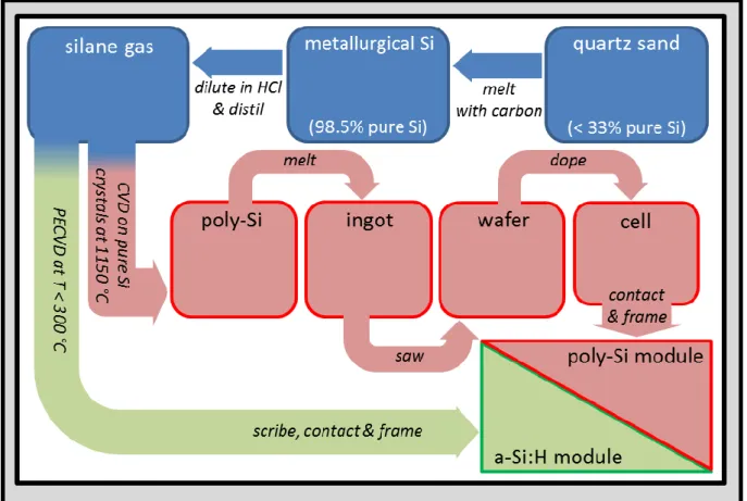
3.1. Breaking down the manufacturing costs of crystalline silicon PV
Over 80% of solar modules on the market in 2011 were made of crystalline silicon.70, 72This material is made from extensively purified and crystallized quartz. The feedstock is initially melted with carbon in an electric arc furnace to remove its oxygen atoms and form 98.5% pure “metallurgical” grade siliconwhich sells for $2-3/kg.75 To remove impurities, the metallurgical grade silicon is diluted in HCl and distilled in the form of chlorosilane vapors which condensate as polysilicon crystals.76 The polysilicon is then melted and gently solidified in the form of a multicrystalline ingot which can reach purities of 99.9999% and prices of $30/kg.71 The material can undergo further purification and melting cycles to ultimately form monocrystalline silicon. Each improvement in purity and crystallinity leads to better electronic properties but incurs extra costs. In 2011 the photovoltaic market was split evenly between polycrystalline and monocrystalline silicon modules.72 The crystalline silicon (whether poly- or monocrystalline) is shaped into ingots and sawed into 180 µm-thick wafers. The material wasted as saw dust during this step can account for up to half the crystalline silicon production. The wafers are doped to establish a PN junction and electrically contacted and connected to create a module. The module is typically encapsulated in a metal frameChapter 1: Introduction
between a sheet of plastic and glass. This manufacturing process for polycrystalline silicon solar cells is schematically illustrated in Figure 1.6.
The cost of each step is difficult to ascertain, but estimates from the NREL Internal Cost Model71 suggest that in a polycrystalline silicon module with a 15% energy conversion efficiency and a price of $1.25/Wp, manufacturing costs are generally divided four ways between purifying the polysilicon ($0.29/Wp), sawing the wafers ($0.32/Wp), making the cells ($0.34/Wp) and assembling them into a module (0.34/Wp).71
1.6 - Silicon PV manufacturing steps.
Manufacturing steps involved in the industrial production of crystalline and thin-film silicon photovoltaic modules.
Figure 1.7 shows that that the building material (the silicon wafer) accounts for roughly half the cost of the photovoltaic module. While other components of the cell may be replaced as the technology matures, the cost of its active layer raw materials offers an indication of the ultimate limit to which its manufacturing costs can be decreased. Attempts to use less refined silicon crystals77 and limit sawing losses78, 79 have been pursued for decades, but their commercial contribution remains marginal to date. Because wafer production is an established industry which has been producing integrated circuits for decades, there are arguably fewer prospects for incremental improvements to dramatically reduce its manufacturing costs.
Chapter 1: Introduction
1.7 - Break-down of manufacturing cost per WP of polycrystalline silicon photovoltaic modules.
Cost estimates for a 15% efficient polycrystalline silicon photovoltaic module fabricated in 2011 inferred from Goodrich71 and Gielen.80
3.2. Short-cuts and hydrogenated amorphous silicon
It is however possible to sidestep wafer manufacturing altogether by depositing silicon directly from the gas phase. This approach was pioneered by David Carlson59 during the 1970s. The gases in question (most commonly silane or silicon tetrachloride) are the same ones distilled from metallurgical grade silicon in Figure 1.6, but the approach obviates the subsequent high-cost crystallization steps. The gas molecules are cracked by plasma enhanced chemical vapor deposition, releasing Si atoms which bond with foreign substrates. The atoms form thin films of atomically disordered material, the most common of which is known as hydrogenated amorphous silicon (a-Si:H). In 2011, a-Si:H-based photovoltaics accounted for 600 MWp of installed capacity.72 Again, the cost breakdown of the technology is tricky to ascertain, but Figure 1.8 combines information from market80 and industry reports81 to offer some general guidelines.
The overall cost per Wp for a-Si:H-based modules ($0.8-1.3/Wp) can be lower than for crystalline silicon ones ($1.2/Wp).80 In addition, the cost of the raw material (silane and dopant gases) used in the active layers of the module is marginal.81 The two main expenses in a-Si:H modules are the depreciation of the equipment used to make the module (notably the plasma deposition reactors),82 and the cost of glass, TCO, metal and other materials required to encapsulate the cell ($0.4/Wp). Some of these materials could ultimately be replaced, for instance by depositing the module on sheets of plastic83 or roof tiles,84 and because a-Si:H has not yet benefited from the same learning curve as crystalline silicon, it offers brighter prospects in terms of reducing manufacturing costs.
Chapter 1: Introduction
1.8 - Break-down of manufacturing costs per WP of thin-film silicon photovoltaic modules.
Cost estimates for a single junction a-Si:H-based photovoltaic module in 2011 inferred from Gielen and Carlson.80, 81
1.9 - Comparing the total cost of polycrystalline and thin-film silicon PV system installations.
Cost estimates for residential photovoltaic systems (installed in Germany using Chinese modules) in 2011. Respective contribution of components inferred from Goodrich71 and Gielen.80
However, these modules suffer from a severe drawback in that their stabilized energy conversion efficiency is typically in the range of 5 – 10%,80 which is considerably lower than the 15% commonly obtained with crystalline silicon. This is important because installing and operating the photovoltaic module requires additional components and services which tend to scale with its surface area, not its power output. Wiring, mounting materials, inverters, batteries, commissioning, installing the panel, maintenance and land can account for 20 to 70% of the final PV system price.71, 80 Less efficient devices incur a higher installation penalty which decisively reduces their competitiveness (Figure 1.9). This is a key area where the photovoltaics sector stands to gain from further scientific research. Amorphous materials and thin-film devices present a wealth of unsolved and scientifically rewarding
Chapter 1: Introduction
questions which could lead to higher energy conversion efficiencies in a-Si:H modules and make their cost benefits more attractive.
Box 4: Alternative thin-film technologies
Hydrogenated a-Si:H is not the only promising new material for photovoltaics. In addition to potential advances in producing cheaper crystalline silicon,77-79 CdTe, CIGS and GaAs modules are also developing rapidly. All three boast higher energy conversion efficiencies than a-Si:H and two of them already occupy larger market shares. However, in all three cases, some of their raw materials (respectively, Te, In and Ga) are in sparse supply. If the dozens of terawatts of global power production are to eventually be supplied by photovoltaics, these technologies will either need to substitute elements of their active layers or engage in recycling operations of unprecedented scales.
Dye sensitized and organic solar cells are also promising technologies but are still tackling issues with chemical stability and are not yet producing modules on the scale of other thin-film materials. Their initial energy conversion efficiencies have reached the benchmark set by a-Si:H85 and the scope for reducing their manufacturing costs could possibly be greater. The issue of off-setting balance-of-system and installation costs by boosting energy conversion efficiency therefore applies to them all the more.
In brief, although the past sixty years have seen tremendous technological and industrial development of photovoltaic cells, the two have not always overlapped. Crystalline silicon, the material which dominates the PV market today, was inherited from scientific breakthroughs predating the space race. Although incremental advances have since improved the efficiency58, 85 and reduced the manufacturing costs of these devices considerably,71, 73 radical innovation will foreseeably be required to drive the cost of solar energy down to grid parity. Novel alternatives include modules based on PECVD deposited a-Si:H which can be produced at lower costs despite the comparatively early stages of their development. However, as the price of photovoltaic systems tends towards their installation costs, materializing the potential of a-Si:H will depend on our ability to improve its energy conversion efficiency. In the following section, some of the causes for the reduced efficiency of a-Si:H-based solar cells are explored and a possible solution is presented.
4. Conducting charges and trapping light in a-Si:H
The main distinction between crystalline and amorphous silicon resides in the arrangement of the atoms constituting the material. To make crystalline silicon, atoms are arranged under high temperatures so as to optimize their bonds in an aligned diamond cubic configuration which can extend over billions of nanometers (Figure 1.10.a). In contrast, because the temperature during silicon PECVD growth is considerably lower, there is less scope for surface diffusion or bond reconfiguration and the atoms generally bond at random. They still adopt covalent bonds, but there
Chapter 1: Introduction
is no order in their distribution beyond lengths of a few atoms (Figure 1.10.b). The short-range order does generate a band structure in the material with an optical bandgap close to 1.8 eV.86 However, it differs from the band structure of crystalline solids in that the conduction and valence band edges are not clearly defined (Figure 1.10.c). This is due to variations in bond angles between atoms, which lead to localized states in an energy range close to the conduction and valence band edges (called Urbach tail states). In addition, the atomic structure locks the occasional Si atom in a configuration which coordinates it to three or five neighboring atoms87 rather than four. The resulting dangling or floating bonds constitute recombination centers (localized states in the middle of the bandgap) which limit the charge diffusion and the doping efficiency of the material.
1.10 - Atomic configuration and density of states in a-Si.
Schematic representation of atoms in crystalline (a) and amorphous (b) silicon. Density of states in a-Si:H depicting the spread of the Urbach states into the bandgap due to disorder in the material and the presence of trap states at the center of the bandgap due to dangling bonds, based on Poortmans and Arkhipov88 (c).
Conduction and doping can be improved in PECVD deposited silicon by adding hydrogen during the growth process to passivate dangling bonds. This results in the formation of a silicon-hydrogen alloy referred to as hydrogenated amorphous silicon (a-Si:H). A fragmented form of crystalline silicon can also be produced by increasing the concentration of hydrogen and the plasma power during PECVD. Silicon atoms then deposit as crystallites embedded in an a-Si:H matrix with diameters reaching hundreds of nanometers and random crystallographic orientations. This material is referred to as hydrogenated microcrystalline silicon (µc-Si:H) and generally has superior conductive properties to a-Si:H, a lower deposition rate and an indirect bandgap. Because the disordered nature of a-Si:H relaxes the quantum mechanical selection rules, the bandgap of a-Si:H is pseudo-direct and the absorption coefficient of a-Si:H is generally larger than that of crystalline silicon.89
Chapter 1: Introduction
Layers of a-Si:H and µc-Si:H can be doped by adding trimethylboron (TMB) or phosphine (PH3) to the silane and hydrogen gas mix during plasma deposition. However, because of recombination centers in these materials, the doping efficiency is lower than in crystalline silicon, requiring higher dopant concentrations to drive the Fermi-level halfway towards the conduction or valence band edges. As this degrades electronic transport, a-Si:H and µc-Si:H solar cells are built by sandwiching an intrinsic layer (which absorbs light and generates charges) between a p-type and n-type layer (which generate the field to separate charge carriers). This architecture is known as a PIN junction. The efficiency of PECVD deposited silicon solar cells can be boosted by stacking a PIN µc-Si:H over a PIN a-Si:H junction in a tandem structure to optimize light absorption in their respective bandgaps.85
Another peculiarity of a-Si:H-based photovoltaics is that prolonged light exposure produces dangling bonds in their material which degrades conductivity.90 This phenomenon, known as the Staebler-Wronski effect, is reportedly less pronounced for thinner91 or more crystalline layers of silicon.92 For a recent review on the subject, we refer the reader to the doctoral research of Ka-Hyun Kim.93 The crucial point which has been tackled in the present thesis relates to the optimal thickness of the intrinsic layer in PECVD deposited solar cells. Although the majority of the above-bandgap solar spectrum can be absorbed in a-Si:H layers about a micron thick,94 minority carriers in the material only diffuse over lengths of a few hundred nanometers95 (compared to hundreds of microns in crystalline silicon).96 This leads to a delicate compromise between charge conduction and light absorption in a-Si:H-based PV devices. A similar question arises with respect to the thickness of intrinsic layers in µc-Si:H solar cells, although more on the grounds of whether gains in light absorption justify increased deposition durations (and hence manufacturing costs). Several drawbacks hindering energy conversion efficiency in cells produced with these promising, low-cost materials are tied to the thickness of their intrinsic layer. Thinning it could increase the electric field across the absorber, improve charge collection, reduce deposition times and minimize Staebler-Wronski degradation. The question is how to achieve this without jeopardizing light absorption in the cell.
4.1. Light trapping and texturing
We have seen that one of the major challenges in a-Si:H and µc-Si:H solar cells lies in making the light absorbing layer thin enough for charges to be collected before they recombine, yet thick enough to absorb the full flux of sunlight. The most common solution is to texture the substrate (typically a transparent conducting oxide) on which the cell is deposited in order to scatter incident light within the plane of the cell (Figure 1.11). This technique is known as light trapping. It relies on differences between the refractive indices of materials in the cell to cause incident light to diffract and reflect at interfaces. Texturing the substrate generally increases the angle of deviation from the initial photon trajectory and hence increases its mean free path through the light absorbing material of the cell.
Chapter 1: Introduction
1.11 - Conventional light trapping in an a-Si:H solar cell.
Schematic description (a) and scanning electron microscopy cross-section (b) of planar solar cell composed of p-type, intrinsic and n-type a-Si:H deposited on a layer of ZnO chemically etched to trap light.
There are several drawbacks to this solution. Texturing the transparent conducting oxide layer generally requires additional manufacturing steps. In the case of a ZnO transparent conductive layer, the vacuum process during which the ZnO is sputtered must be interrupted to dip it in a chemical etchant before it is returned to vacuum in order to deposit the subsequent layers of the cell. Another problem is that the random structures obtained on rough transparent conductive oxide layers continue to reflect part of the incident light and are transparent to a considerable fraction of lower energy photons. The approach also imposes an additional constraint on the transparent conductive oxide layer which must already be engineered for high optical transmission, chemical stability and high conductivity. These properties are often in competition (e.g. what improves the layer transparency can degrade its conductivity) and it would be preferable to relieve the layer from the burden of texturing.
One alternative is to texture the silicon itself. This approach has been used for decades to increase light trapping in crystalline silicon cells in which the cell surface can be inclined with respect to incident light by etching pyramids or grooves out of the wafer. A more radical variant of this idea is to incline the entire PN junction with respect to the angle of light incidence so as to maximize the surface texture of the cell without increasing the distance over which charge carriers drift to be separated. This has been achieved for instance by etching areas of ZnO layers over which conformal layers of silicon are deposited.98 However, these approaches all imply additional manufacturing steps which waste useable material. Ideally, the whole cell would be grown from the start in a three-dimensional configuration and with regions of different refractive indices penetrating through its entire thickness to maximize the effect of light trapping. Over the past five years, this ideal has grown increasing plausible with advances in the fields of silicon nanowire growth and radial junction solar cells.
Chapter 1: Introduction
4.2. Silicon nanowires and the radial junction solar cell
The objective of radial junction silicon solar cells is to absorb more light in thinner layers of material using highly textured surfaces. However the technique used in this case is to fabricate (e.g. p-type) doped pillars of silicon and cover them in intrinsic and (n-type) doped conformal layers of silicon (Figure 1.12). This is a particularly interesting approach for a-Si:H and µc-Si:H solar cells as pillars fitting this description can be fabricated directly by PECVD in the form of silicon nanowires. We will look closer into how silicon nanowires are made in Chapter 3. For now suffice it to say that, during chemical vapor deposition, drops of metal can locally enhance the deposition rate of silicon from the gas phase. This leads to the formation of vertical, cylindrical structures known as silicon nanowires. Arrays of these nanowires can present highly textured surfaces which have been observed to absorb light remarkably well.99-104 The advantage of using SiNWs to texture PECVD deposited solar cells lies in that remarkably textured devices can be produced in a single deposition run.
1.12 - Light trapping in a radial junction solar cell.
Schematic description (a) and scanning electron microscopy image (b) of a radial junction solar cell deposited over p-type PECVD-grown silicon nanowires designed for light trapping and covered in intrinsic and n-type layers of a-Si:H.
A full history of how radial junctions reached their current state of development is offered in Chapter 5. Here we simply highlight that at the time that we began to investigate this technology, numerous technical problems remained unsolved. The first attempts at making SiNW-based radial junction devices had led to low short-circuit currents,50, 105-108 leaving open to debate whether most of the light which they scattered was being absorbed in the cell rather than in surface states101 or in remnants of the metal particles that catalyze their growth. The cells also suffered from unexplained voltage losses compared to their planar counterparts, with open-circuit voltages typically reaching 300 mV.105, 106, 109, 110 These flaws raised serious questions over the practicality of SiNW-based radial junctions for photovoltaics - questions which we intend to answer in the following four chapters.