Open Archive TOULOUSE Archive Ouverte (OATAO)
OATAO is an open access repository that collects the work of Toulouse researchers and
makes it freely available over the web where possible.
This is an author-deposited version published in :
http://oatao.univ-toulouse.fr/
Eprints ID : 18042
To link to this article : DOI:
10.1016/j.microrel.2015.12.020
URL :
http://dx.doi.org/10.1016/j.microrel.2015.12.020
To cite this version :
Bensoussan, Alain How to quantify and predict
long term multiple stress operation: Application to Normally-Off
Power GaN transistor technologies. (2016) Microelectronics
Reliability, vol. 58. pp. 103-112. ISSN 0026-2714
Any correspondence concerning this service should be sent to the repository
administrator:
[email protected]
How to quantify and predict long term multiple stress operation:
Application to Normally-Off Power GaN transistor technologies
A. Bensoussan
1Institut de Recherche Technologique Saint Exupery, Department More Electrical Aircraft, Toulouse, France
a b s t r a c t
The present paper is implementing a numerical application of the Boltzmann–Arrhenius–Zhurkov (BAZ) model and relates to the statistic reliability model derived from the Transition State Theory paradigm. It shows how the quantified tool can be applied to determine the associated effective activation energy. The unified multiple stress reliability model for electronic devices is applied to Normally-Off Power GaN transistor technologies to quantify and predict the reliability figures of this electronic type of product when operating under multiple stresses in an embedded system operating under such harsh environment conditions as set for Aerospace, Space, Nuclear, Submarine, Transport or Ground application.
Keywords:
Wide band gap semiconductor III-nitrides
GaN GaN-on-Si Design-for-Reliability Reliability
Transition State Theory Quantum statistics
Maxwell–Boltzmann distribution
1. Introduction
The model of the Transition State Theory (TST) developed by E.
Wigner[1]and M. Evans and M. Polanyi[2]in 1938 was considered to
derive the unified reliability theory presented. Accordingly, the failure rates and reliability mathematics for Cumulative Distribution Function (CDF), Reliability function (R) and Probability Density Function (PDF) have been described when considering the TST concept. In former pa-pers we have demonstrated how multiple stresses applied, may impact
the effective activation energy suggested by the BAZ model[3,4]. We
will see here how to apply the pre-defined model to the case of a Gallium Nitride Normally-off high power transistor (Enhanced-mode) and a detailed numerical application. The quantified tool will be applied to determine the minimum value of stressor parameters named χ's and the equivalent single associated minimum effective activation energy to predict long term operation under multiple stresses in harsh environ-ment. The completed numerical application on a Normally-off transistor GaN reference GS66508P-E03 650 V enhancement mode manufactured by GaN Systems is proposed to support the methodology. The concepts of maximum rating limits and burnout conditions are key factors which will give insight to derive related stressors as parameters χi's and γ's, both statistically represented by a normal distribution law.
The paper is organized as follows: after a recall of the principle of the generalized BAZ model, we will take the example of a Normally-Off GaN Power transistor detailing from the data sheet the maximum rating limits and will show other dynamic maximum rating limits to be con-sidered in detail mainly related to the switching bias operation condi-tions (also related to design rules). Finally the BAZ model will be refined and adapted to this technology. A short discussion will recall the main highlights we have observed.
2. BAZ model and Transition State Theory
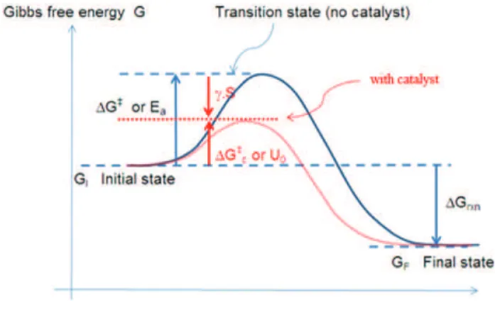
Shown inFig. 1, is a free energy diagram of why things generally
tend to degrade faster at higher temperatures as explained in chemistry
and Reliability Physics books (see for example J.W. McPherson[5]).
Stress-dependent activation energy observations seem to be general in nature (i.e., not confined just to a single failure mechanism or stress type), and works attempt to explore the conditions under which a stress dependent activation energy is theoretically expected. The generalized Eyring model presented by McPherson has been refined under the
BAZ model[3,4].
Fig. 1is simply related to the general model called Boltzmann–Ar-rhenius–Zhurkov (BAZ) also described by the Transition State Theory
(TST)[1,2]. We have seen the stress factor γ. S can precisely
counterbal-ance the Arrhenius activation energy Eafor a device at burnout due to an
overstress (i.e. the energy of the transition state with burnout catalyst effect is at the same level as the initial state energy). In this case this
E-mail address:[email protected].
1Permanent address: Thales Alenia Space France, Competence Center Electronics
(CCEL), Toulouse, France.
works for any failure mechanism that is thermally determined as a rate function described by the Maxwell–Boltzmann distribution.
We have expressed the BAZ model as the lifetime τ defined by the following equation: τ¼ τ0" exp Ea k " Teff" c χð i" γiÞ ! " ð1Þ
With a dimensionless energy factor parameter c(χi⋅ γi) given by:
c χð i" γiÞ ¼ 1−k " T eff
EA "
XM
i¼1ðχi" γi" SiBOÞ ð2Þ
where the SiBOis the corresponding maximum catastrophic burnout
failure limit related to each electrical stress parameter for i = 1 to M
(current, voltage and power), Teffis the absolute temperature that
could depend also on the applied stress χiwhen the Joule effect is
occur-ring, τ0is the time constant, and γiis the factor of loading characterizing
the weight of the level of stress. This equation is seen as the
generaliza-tion of the Eyring model as demonstrated in[2]. Indeed, when the stress
parameter is set to SiBOleading to a sudden catastrophic failure we have:
χi= 1 and c(1) = 0 allowing calculating γifor a combination of
stress parameters as: Ea¼ k " Teff"
XM
i¼1ðγi" SiBOÞ: ð3Þ
Because every χiis in the range [0; 1], this equation shows that the
activation energy is compensated by a linear combination of stressor energies associated with each parameter.
When considering the simplest configuration where the main
stress-or is the breakdown voltage characterized by a term χV, suppose other
stressors χjto be equal to 0. Eq.(4)for χV= 1 will allow determining
γVas:
γV¼
Ea
k " Teff" VBO ð4Þ
Combining Eqs.(4) and (2)leads to:
c χð V" γVÞ ¼ 1−χV: ð5:aÞ
We have seen similar equations can be obtained for other stressors when considered alone:
for pulse power dissipation2
c χð P" γPÞ ¼ 1−χP ð5:bÞ
for current
c χð I" γIÞ ¼ 1−χI: ð5:cÞ
Because the principle of superposition is not valid, it is understood that the situation is different when considering a multiple stressor configuration applied simultaneously.
Considering the situation of three stressors: a) χIrelated to current
limited by the maximum allowed current characterized by IBO, b) the
breakdown voltage characterized by a term χVand VBO, and c) stressor
χPrelated to power consumption related to the maximum allowed
dissi-pation characterized by PBO.
Saying Eqs.(5.a),(5.b)and(5.c)are constrained by the boundary
conditions defined for the burnout limits (subscribe BO), we obtained: c χð i" γiÞ ¼ 1−k " Teff
Ea " γ½ð I" χI" IBOþ γV" χV" VBOþ γP" χP" PBOÞ'
: ð6Þ
Merging Eq.(6)with Eq.(4), we were able to normalize burnout
parameters and we got an expression of coefficient c(χi; γi):
c χð i" γiÞ ¼ c χð I; χV; χPÞ ¼ 1−χI−χV−χP: ð7Þ
The simple schematic drawing given inFig. 2details contributions of
stressors when three stressors are simultaneously applied as per Eq.(7).
The next chapter will show how a numerical application on a Power GaN Normally-Off transistor enhancement mode GaN transistor is implemented.
3. A Normally-off transistor GaN: data sheet and maximum rating definitions
As an example, the data sheet given (at the date of this publication) in
Table 1defines the parameters extracted from a Power GaN Normally-Off transistor GS66508P-E03 650 V enhancement mode GaN transistor
(reproduced from data sheet GaN Systemswww.gansystems.com).
Generally, maximum rating limits are defined and are considered
with a given margin compared to burnout failure limits (MI, MVor MP
respectively for current, voltage and power dissipation).
Sudden catastrophic failures due to electrical overstresses can be characterized for each transistor lot. This consideration will help to define the sine qua non condition to consolidate the reliability model.
2 Pulse power dissipation or commutation losses needs (turn-on and turn-off energies)
to be considered when using such Normally-off transistors in their application because of the switching time conditions from off-state to on-state operation can stress the device close to the limit of its SOA in pulsed mode.
Fig. 2. Schematic of equivalent effective activation energy w.r.t. three stressor contributions.
Multiple stresses can be seen as a juxtaposition of stress amplitudes (not the superposition principle) leading to reduce proportionally the effective activation energy up to a zero value maximum limit (in this case the activation energy is exactly compensated by the cumulated stress factors). Let's consider the following notation for burnout conditions (also supposed to be described by a normal distribution) (seeFig. 3for labeling conditions compared to the Safe Operating Area (SOA)):
Off-state drain current VDSoff-BO(condition3)
• On-state drain current at saturation IDSon-BO(conditions1,2&4),
• Maximum power dissipation during on-off nominal operation PDS-DC-BO(conditions 5 and 6 to 8).
When conducting evaluation and qualification testing sequences as depicted in MIL Standards or similar, such DC stress tests are foreseen. We propose to implement such qualification test sequence and biasing
depicted inFig. 3 in the frame of the Robustness project we are
conducting. The results will be presented in another paper in a future study. But indeed, they have several drawbacks:
a) They are focused on validating simple stress conditions including high temperature stress superposed with a single DC bias stress at a time, b) They are based on the Arrhenius law considering accelerating factors managed by high temperature effects forgetting low temperature effects,
c) They generally don't address dynamic stress conditions (even RF or switching in operation) at high or low temperature.
SOA limits are defined for DC stresses but are half-finished when considering nominal operating conditions. They must be completed by switching stress conditions to be imposed to the designers. In order to highlight how the design rules must be taken into account, the next paragraph will provide such major inputs.
4. A Normally-off transistor GaN: reliability impact of turn-on/ turn-off switching voltage induced by commutation losses
Since Normally-off GaN transistors start to conduct significant
cur-rent at VGS(th) = 1.6 V, care must be taken to ensure a low impedance
path from gate to source when the device needs to be held off during dv/ dt in a rectifier function. As the temperature coefficient of the eGaN FET is positive throughout its range of operation, this means that when the temperature of a localized region of the device increases, its current car-rying capability is reduced causing the current to be dispersed to other areas of the die. This dispersion of the current equalizes the temperature of the die, and is known as “self-ballasting.” The power MOSFET, on the other hand, has a significant region of negative temperature coefficient operation (below 5.0 V on the gate) where there is no self-ballasting.
Table 1
Example of preliminary data sheet of GS66508P-E03 650 V enhancement mode GaN transistor. Reproduced from GaN Systemswww.gansystems.com.
Symbol Parameters Value Units
Absolute maximum ratings (at Tcase = 25 °C unless otherwise noted)
TJ Operating junction temp. − 55 to + 150 °C
TS Storage temperature range − 55 to + 150 °C
VDSmax-rating Drain-to-source 650 V
VGS Gate-to-source ±10 V
IDS(cont)25(or IDS-MR) Continuous drain current (Tcase = 25 °C) 34 A
IDS(cont)100 Continuous drain current (Tcase = 100 °C) 20
ID,pulse(or ID-pulse-MR) Pulsed drain current (Tcase = 25 °C) (note 1) 45 A
Note 1: Limited by saturation
Thermal characteristics (typical values unless otherwise noted)
RθJC Thermal resistance (junction to case) 0.5 °C/W
RθJA Thermal resistance (junction to ambient) 55 °C/W
Device mounted on PCB (see corresponding datasheet for detail)
Electrical characteristics (at Tcase = 25 °C unless otherwise noted)
Symbol Parameters Typ. value Units Conditions
BVDSS Drain-to-source breakdown voltage 650 V VGS = 0 V, ID= 3.3 μA/mm
RDS(ON) Drain-to-source on resistance 52 mΩ VDS= 7 V, TJ= 25 °C, ID= 9 A
VGS(th) Gate threshold voltage 1.6 V VDS= VGS,
ID= 7 mA
IDSS Drain to source leakage current 2 μA VDS= 650 V
VGS= 0 V, TJ= 25 °C
IGSL Gate to source leakage 200 μA VGS= 7 V,
VDS= 0 V
Vplat Gate plateau voltage 3 V VDS= 400 V
VSD Source–drain reverse voltage 3.0 V VGS= 0 V, TJ= 25 °C, ISD= 9 A
Fig. 3. Safe operating area of Normally-Off GaN transistor showing boundary conditions defined for χ and γ parameter determination.
Operation within this region creates localized hot spots within the die and, thus, limits the SOA capability of the die.
These considerations have been explained on literature by B. Cogo
et al.[6,7]and J. Brandelero et al.[8]. From these papers, power device
modeling published articles have shown turn-on turn-off switching voltage characteristics induced by commutation losses. Losses in the switches are usually the most important point to be considered in a con-verter design; however, switching losses are not always provided in datasheets. The following text is mainly inspired from large extract from the three papers.
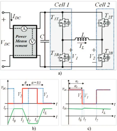
As implemented in[7], turn-on and turn-off energies could be
accurately determined separately for different switched voltages and currents by controlling the commutation of a full bridge in two different modes. The authors argue that due to the packaging of GaN EPC© devices, current measurement into device is not possible with a Rogowski probe or a current transformer without changing the power loop. This is also the case for almost all low voltage Silicon MOSFET packaging. Since the opposition method is a non-invasive method, it is suitable to be used to measure switching losses of “wide bandgap” devices. The opposition method consists of an association of two identi-cal converters supplied by the same source, one operating as a
genera-tor, the other as a receptor (as shown inFig. 4). Thus, a test bench
using the opposition method was implemented in[8]to characterize
switching energies, under actual working conditions, of an EPC1001 GaN power transistor. Consideration of such commutation (ripple)
induced stresses is presented in Fig. 5, showing an overview of
switching losses in a buck converter operating in two different modes: low current and high current ripple modes.
The authors have considered other losses as listed below: • Inductor losses,
• Transistor conduction losses, • Connection losses,
• Bus capacitor losses.
Taking into account such parasitic effects, we propose to introduce three (3) new stress factors at burnout failure limits which can be responsible for impact and degrade effective activation energy, including:
• Turn-off controlled commutation
o Energy turn-off dynamic switching Eoff-surge(energy factor χEoff-surge),
• Turn-on controlled commutation
o Transistor turn-on energy Eon_surge, which includes the reverse
recovery losses of the body diode (energy factor χEon_surge)
o Turn-on dynamic switching for VGS-surge(energy factor χVGSon_surge).
Recalling chapter II and these parasitic effects, we can express the energy factors as a juxtaposition of stressor parameters as listed in
Table 2each of them defined by their γ parameters and their associated
χ's bounded by their maximum rating limits calculated from Eqs.(4)
and(5.a),(5.b)and(5.c). To do so, activation energy related to the
Fig. 4. a) Circuit used in the proposed method to measure switching energy of transistors, b) typical voltage and current waveforms for the “turn-off loss measurement mode” and c) for the “turn-on loss measurement mode”.
ohmic contact (TiAl:GaN system based alloy) and Schottky contact (TiN:GaN system alloys) are considered for EPC technology.
As summarized by Del Alamo in 2009[9], relatively high activation
energies have been reported from 1.05 to 2 eV for GaN technologies. This paper highlighted an electrical degradation mechanism for GaN HEMTs that is associated with the strong piezoelectric nature of GaN and AlGaN. Under high voltage conditions, the high electric field that is produced introduces strong tensile stress in the AlGaN barrier layer that peaks right below the gate edge. This results in an increase in stored elastic energy inside the AlGaN. If exceeding a critical value, crystallographic defects are formed that are electrically active. The damage consists of dim-ples, cracks crystallographic damage on the drain side of the device right
next to the gate edge. These have shown the presence of prominent that ex-tent through the AlGaN but stop at the GaN interface and, in extreme cases, metal diffusion from the gate down the crack. In addition, the level of crystallographic damage correlates with the degradation in the electrical characteristics of the device.
Linking to Eq.(3), and as a preliminary analysis, let's consider the
activation energy associated with metallurgical diffusion mechanism as the main effect characterized by a value close to 2.1 eV. Of course this value must be assessed and confirmed on a given GaN technology process after a series of simple high temperature storage test sequences.
The effective junction temperature Teffmust also be related to the case
temperature and the thermal resistance of the junction case.
Fig. 5. Ideal Hard Switching (extracted from EPC WP009) for a) turn-off transition, b) turn-on transition, c) typical turn-off energy calculation (from[8]) based on switch voltage and current and d) measured switching energy for different switched currents and voltages, for the 100-V eGaN FET EPC1001.
Table 2
List of the 10 stressor parameters and related values used impinging on the effective activation energy applied to GS66508P-E03 650 V enhancement mode GaN transistor (assuming Ea
and Teff— see detail in text).
Parameter Maximum rating values (MR) DC limit BO DC BO values Dynamic biasing stressors
Surge BO limits Transient stressors Transient BO limits γ (Eq. 4) Calculated γ values at Teff= 298 K χi MR
1 Current IDSon 34 A IDSonBO 68 A γIDSon 1.20 50%
2 IDSon_dyn
(@ 10 μs)
45 A IDSon_sgeBO 90 A γIDSsge 0.91 50%
3 Voltage VDSoff 650 V VDSoffBO 900 V γVDSoff 0.091 50%
4 VGSon
(@ IDSonMR)
10 V VGSon_sgeBO
(@ 10 μs)
20 V γVGSon 4.09 50%
5 Power PDSonDC 235 W PDSonBO 470 W γPDSon 0.17 50%
6.1 PonDYN 402 @ 300 μs Pon300BO 574 W γPonDYN300 0.14 70%
6.2 750 W @ 100 μs Pon100BO 1072 W γPonDYN100 0.076 70%
6.3 2680 W @ 10 μs Pon10BO 3830 W γPonDYN10 0.021 70%
7 Energy EoffDYN 7 μJ Eoff_sgeBO 20 μJ γEoff_sge 4.09 35%
Calculated values for γ at Teff= 298 K (Eq. (3)) and χiMR(Eq. (4)) are
completed in Table 2 (assuming the Boltzmann constant k =
8.61733 ⋅10−5 eV⋅K−1) and E
a= 2.1 eV. These parameters are related
to burnout parameter limits from which we know they are character-ized by a Gaussian or Standard distribution law. Consequently each of them can be written in terms of mean and standard deviation factor as follows: fsd SiBOfailure $ % ¼ 1 σiBO" ffiffiffiffiffiffi 2π p " e− 1 2
SiBOfailure−SiBO σ iBO
' (2
ð8Þ
where siBO and σiBOare respectively the mean and the standard
deviation of statistical distribution law of every SiBOfailure.
5. BAZ model applied to Normally-off GaN transistor
As a result the related parameters χi's are statistically represented by
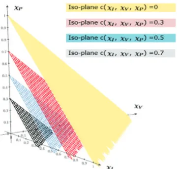
a similar distribution law andFig. 7represents a 3D-plot of such
normal-ized stress factor χivs the catastrophic burnout limit SiBO_failureof a
Normally-off transistor GaN. When a parameter failure limit is affected by the temperature as for example observed on breakdown voltage
decreasing when the temperature is decreasing[10], this effect can be
easily considered within the reliability model thanks to the γV
parameter.
In this example we have considered normalized stress conditions
and we can see the behavior of the coefficient c(χI, χV, χP) for three χP
values (from 0 to 0.5) and varying χIand χVfrom 0 to 1. Having such
a mapping, we need to consider that the χiparameters are limited by
their maximum rating values as given inTable 3and thus the value
achievable by the coefficient c(χI, χV, χP) is quantified when multiple
stresses are combined. Accordingly the related triplet (χI, χV, χP) can
be calculated and a new reliability criterion can be drawn which relates
simply as a single condition all constraints associated with Ea, all
derating limits (both statics and dynamics) and thermal condition. We
propose to set coefficient c(χI, χV, χP) verifying:
c χI;χV;χP
$ %
N30%: ð9Þ
This value is chosen in order to guarantee an effective activation energy greater or equal to 0.7 eV for a worst case wearout failure mechanism. In such a case, to demonstrate long term life in operation
for Space Application as shown inFig. 6, we will need to run sampling
devices under biasing for a 3000 hour endurance lifetest sequence at
Teff= 280 °C (to achieve 80% lot failure) in order to be equivalent to
30 years at Teff = 110 °C (for 0.1% failure). Note that this is equivalent
to MTTF (@110 °C) = 1.5 million hours or more than 170 years. Now, we can draw the major conclusion of this section that is: when multiple stresses are applied simultaneously, the derating parameters and their maximum rating limits values need to be set in order to counterbalance an equivalent activation energy not inferior to 30% of
Ea. Iso-planes c(χI, χV, χP) = constant, are shown inFig. 7and represent
combination of triplet rates to get a given value of c(χI, χV, χP) in view to
satisfy a foreseen activation energy goal.
The drawing inFig. 8 presents the methodology to determine
operating worst case conditions which can be supported by the device
under operating conditions and environmental multiple stressors in order to guarantee a time to failure rate of less than 1% after 30 years
at junction temperature lower or equal to 110 °C as shownFig. 6.
In the same spirit we defined the stressor energy concept (γ linearly proportional) and we can introduce a new concept for the internal en-ergy of a device to be a straightforward linear relation with the electrical mode under consideration. Gradual degradation or sudden catastrophic ones are evidenced and signed by electrical failure modes. In the follow-ing we will try to define the mathematics of this perception.
6. A numerical application example for a Normally-off GaN transistor
In the following we are assessing the multi-stress induced effect the reliability figures on a GS66508P-E03 650 V enhancement mode Normally-off GaN transistor. The Arrhenius activation energy due to
thermal stress only is assumed to be Ea= 2,1 eV.
Table 3
Electrical parameter limits for voltage and power stressors.
Parameter limits VDSoff PDSoff
@ Burnout (a) 900 V 470 W @ Maximum rating (b) 650 V 235 W @ Derating limits (c) 487.5 V 117.5 W Χioff(c)/(a) 54.2% 25%
Fig. 6. Probability of failure vs Teffand time t (assuming Eaeff= 0.7 eV). The lifetest
sequence proposed on top will demonstrate less than 0.1% failure at 110 °C after 34 years).
In order to assess the reliability model and to define the limits of the Safe Operating Area (SOA) we need to define some specific condition of endurance testing with high enough stress to accelerate failure mechanisms.
Future reliability test programs are designed in order to simulate and accelerate various failure mechanisms one at a time. Power converter equipment based on Normally-Off GaN transistors as shown in
Section 4are designed in order to minimize to a less extent the commu-tation losses. Switching conditions between off and on states with short transition time are implemented but such losses cumulated during operation may generate multiple stress behavior. In order to simulate such operation we can design a reliability test program with two
kinds of stress test at high VDSoff. The BAZ model proposed helps to
simulate such occurrence of multiple stress conditions and to take into account their interactions.
Let's consider two types of stresses imposed simultaneously: a. the off-state at VDS close to the breakdown voltage or close to
burn-out of the transistor: i.e. the Voltage stressor
b. the IDScurrent at high VDS induced during the switching time which
can be set under equivalent static condition to simulate the Joule effect induced by commutation losses: i.e. the Power stressor.
The following will explain how to handle these stresses in parallel and to assess the combined activation energy to be considered for accel-erating factor determination.
Space industry defines maximum rating and associated derating condition for safe operation in use as the following: voltage should
never exceed 75% of the maximum rating of any voltage (VDSor VGS)
and currents (IDS) and never exceed power dissipation greater than 50%
of the maximum rated power dissipation. In addition to that Tjunction
must remain lower than 110 °C during the flight mission.
As per data measurements performed of COTS samples on the GaN
transistor GS66508P-E03 650 V we obtained the followingTable 3:
Eq.(7)factor c(χi; γi), gives the value of this term when mechanisms
Voltage Stressor and Power Stressor are applied:
c(χi; γi) = 1 −54.2% −25% =20.8%..
When the two stressors are applied simultaneously at their derating limits, the effective activation energy is reduced to 0.437 eV. Such activation energy is reducing drastically MTTF foreseen for Space appli-cation and then even compliant to Space rules the MTTF is no more acceptable.
When stressor percentages are lowered by reducing VDSvoltage to
330 V and Pdiss to 140 W their contribution to the effective activation
energy is 33.6% of Ea(i.e. 0.7 eV) as shown inFig. 7. In other words
this model helps to assess the impact of the mission profile on the final activation energy expected and then assesses margin to Design for Reliability Space equipments. We need to be very careful when ap-plying Quality Standards which are not considering multiple-stressor impacts and new rules for HiRel application are recommended to be set accordingly.
7. The BATHTUB curve model
Considering N “good” devices of interest randomly selected from a homogeneous manufacturing lot. The term “good” means the devices are non-discernible, they are functional and their performance and elec-trical parameters are statistically normally distributed (Gauss or Normal statistics). Let's consider the most representative electrical parameters (biasing or leakage currents, biasing or breakdown voltages) to be a rep-resentative sensor of the healthiness of the devices. For the sake of sim-plicity, we focus on the failure mode used for reliability consideration which is the most representative electrical parameter. Such a parameter can be considered as a signature or saying a measure of the internal
energy ϵ as referred inFig. 9where for example be the pinch-off drift
of a GaAs MESFET technology plotted as a square root of time
degrada-tion mechanism (gate sinking metal diffusion in active layer). ThisFig. 9
is a schematic drawing of the TST and applied to the reliability of
electronic parts showing how the BAZ model is applying. Other mecha-nisms as Early Failure or Infant Mortality and Random Failures are positioned as they may occur earlier assuming different gradients of degradation time (assumed to be linear or super linear).
7.1. How to determine the distribution function or the probability for a device at energy state ϵ.
Because devices are characterized by their electrical parameters measured experimentally we have a physical indicator tool to quantify the energy change during aging and saying the drift of a parameter
failure mode ΔEFM/EFM0is directly linked to the internal energy as:
ε tð Þ ¼ −α1" kT ΔEFM t ð Þ EFM0 ! ð10:aÞ σεð Þ ¼ αt 2" σEFMð Þt ð10:bÞ
where EFM0is the electrical parameter measured at t = 0. ΔEFM(t) and
σ(t) are respectively the mean and the standard deviation of electrical parameter (Gaussian distribution) depending on aging time.
Eqs.(10.a) and (10.b)are supported by the fact that Free energy of a device is proportionally increasing with temperature; when the failure mode degrades. Consequently, the Free energy increases with time (the sign “−” is introduced because percentage of parameter drift is negative). Thus, the probability density function is now assumed to be a func-tion of the energy at time t described by a Gaussian distribufunc-tion law:
f ε;ð tÞ ¼ 1 σεð Þ "t ffiffiffiffiffiffi 2π p e− 1 2" ε−ε tð Þ σ ε tð Þ $ %2 : ð11Þ
Knowing this probability density function and recalling the set of equations we are able to model:
A) Wearout failures based on:
• The number of failed device at time t assumed to be Wearout failure:
NFailð Þ ¼t
Z∞
U0−γ"S
ρwearoutð Þ " fε wearoutðε;tÞ " dε: ð12Þ
• The number “Good” devices defined by:
NGoodð Þ ¼t
ZU0−γ"S
0 ρwearoutð Þ " fε wearout ε;
t
ð Þ " dε: ð13Þ
• The normalization when considering the total number of device is given by: NTð Þ ¼ Nt Goodð Þ þ Nt Failð Þ ¼t Z ∞ 0 ρwearoutð Þ " fε wearoutðε;tÞ " dε: ð14Þ B) Random failures:
• Random failure mechanisms can be discriminated versus time in Eqs. (12) to (14)considering that the appropriate distribution
Fig. 9. Effect of failure phases (Early, Random and Wearout) deduced from Transition State Theory.
function or probability that a device at energy state E is defined by a
function of energy frandom(E) and assuming the adequate density of
states, or the number of energy states per unit volume in the interval
ΔE is ρrandom(E).
C) Infant mortality model
• Infant mortality is defined by Eqs(12) to (14)considering that the
ap-propriate distribution function or probability that a device at energy
state E is defined by a function of energy finfant(E) and the adequate
density of state or the number of energy states per unit volume in
the interval ΔE is ρinfant(E).
Early failure, random failure and wearout mechanisms can be
discriminated with time thanks to Eqs.(12), (13) and (14)respectively
accommodated in order to depict the full bathtub curve. Doing so, the Instantaneous Failure Rate (IFR) λ(t) is defined by:
λ tð Þ ¼NNFð Þt Tð Þt ¼ Z ∞ U0−γ"S ρ ε;ð tÞ " f εð ;tÞ " d Z ∞ 0ρ ε; t ð Þ " f εð ;tÞ " d ð15Þ
with the corresponding superposition of failure mechanisms and their appropriate definitions.
All these equations are linked to the suitable densities of state ρinfant(E), ρrandom(E) and ρwearout(E). Appendix A is describing how
such densities of state can be calculated and quantified based on a Maxwell–Boltzmann statistical approach.
8. Discussion
The generalized BAZ model based on simultaneous multiple stress conditions has been presented and is fully depicted thanks to consider-ing absolute maximum ratconsider-ings and burnout limit normalization. The
methodology implemented for the GaN transistor process inSection 5
can be easily generalized to any type of electronic device for any failure mechanism that is thermally determined as a rate function described by the Maxwell–Boltzmann distribution.
To complete our study, here are some views related to advantages and comments of the proposed methodology.
To illustrate this, let's considering Hot Carrier Injection mechanism and impact ionization stress mechanism. They are mostly observed to have higher failure rates at low temperature than at high temperature. Hence, negative activation energy must be set for low temperature range while positive activation energy must be introduced for high tem-perature range.
The BAZ model is a single effective activation energy representing no more than one effective mechanism. For multiple activation energies, we have to consider that the multiple mechanisms are statistically inde-pendent and they must be dealt with a stochastic process. This will allow the total equivalent failure rate at any temperature and/or combi-nation of stresses to be a sum of FIT. This is exactly what the approach
proposed by J. B. Bernstein[11,12]is offering as related to the Multiple
High-Temperature Operating Life (M-HTOL) test. It can certainly be an outstanding combination with the BAZ model. This merging will be studied and developed in a future paper in preparation with J.B. Bernstein.
8.1. Advantages
The Transition State Theory was set in the generalized BAZ model. It helps to elaborate a useful tool aiming to develop a methodology to
define, quantify and predict the complete reliability Bathtub curve for any electronic device. Furthermore, it takes into consideration a combi-nation of multiple stress conditions merging intrinsic and extrinsic constraints and electrical modes. It provides a good simple support to model the catalyst effect induced by many stressors as for example ther-mal and dynamic biasing or radiation stresses. Anticipating combined effects due to various stressors, we have shown how efficient is the model applied to new emerging technologies as GaN processes: helping to quantify and reduce evaluation and qualification test time sequences. There is no need to conduct multiple stress test sequences rather it is proposed to perform only a simple storage stress associated to deep electrical characterization and develop a good knowledge of physics of failure (based on very detailed constructional analyses and failure anal-ysis methods).
The generalized BAZ model takes into consideration other stressors than temperature defining accelerating factor for DC and AC parameters in a simultaneous combined form. It is applicable to support low temperature acceleration models as well.
Finally, the model is easy to be implemented and consolidated and provides a useful tool for determining and recommending design rule consideration for breakthrough technologies: it covers Design for Reliability methodologies as required in the Prognostics and Health Monitoring (PH&M) paradigm.
The generalized BAZ model is an extension of the Arrhenius law not only applicable to diffusion and storage test stresses but also valid for other combined harsh environment stressors cumulated with temperature.
8.2. Other comments
Of course the generalized BAZ model is supported by the hypothesis that the internal energy of a device is perceived or observed by an elec-trical mode signature: either a leakage current of a performance param-eter. This is not always the case as some hidden failure mechanisms can be activated (i.e. not seen as continuous electrical degradation but rath-er as sudden catastrophic failure). This is noticed for latent (cumulated or not) effects (due to contaminants, ESD, EOS, increase of dislocation density, radiation as displacement damage DD for example) or even for crystal dislocation accumulation in active and non-active regions. When these physical and/or electrical precursors are not yet active, they can be later activated by temperature and electrical stressors.
In all these particular cases, the generalized BAZ model is failing or less accurate to predict failure and the end of life limit. If so, the Early Failure or the Random Failure stages of the Bathtub curve can be overestimated. On the one hand, one needs to identify failure analysis techniques or electrical characterization method to pinpoint electrical precursors to model the behavior of the reliability. On the other hand, it is necessary to collect and validate how the stressors are acting to ac-celerate the failure mechanisms expected.
These limitations of the generalized BAZ model will require some re-finement or new techniques of characterization to be instigated. We will address such considerations in our future studies and in particular for the case of small size node (lower than 30 nm) of Si semiconductor integrated processes called Deep-Sub-Micron (DSM) technologies. 8.3. Special care to be considered when applying this methodology — how to consolidate it?
Existing and new failure analysis techniques need to be controlled and implemented. Similarly, constructional analysis and knowledge of semiconductor physics modeling are pre-requisites in any case. These two prerequisites will let us understand failure mode created under dynamic operating conditions. The use of such emerging and non-stabilized technologies imposes careful implementation of adequate Design Rules. In particular, dynamic stress (switch off and switch on inducing losses) for implementation of GaN Power Switch transistor
devices is of particular concern and can be viewed in light of such gen-eralized BAZ methodology proposed. As a consequence, design and reli-ability simulation tools are important threads to be under control. Design rules as well as electrical and physical characterizations are key phases to be structured.
9. Conclusion
The principle of the generalized BAZ model exposed in Ref.[2]was
recalled. An example of a Normally-Off GaN Power switch transistor de-tailing from the data sheet the maximum rating limits was considered. We have seen how other dynamic maximum rating limits must be pon-dered in detail and in particular for switching bias operating conditions (also to be related to specific Design Rules to define).
The generalized BAZ model was refined and adapted to the GaN technology. As an example we have completed numerical Application on a Normally-off transistor GaN reference GS66508P-E03 650 V en-hancement mode manufactured by GaN Systems. The concepts of max-imum rating limits and burnout conditions have been useful to derive
key parameters as χi's and γ's, both statistically represented by a normal
distribution law. In particular such normalized stress factors χivs the
catastrophic burnout limit SiBO_failureof a Normally-off transistor GaN
were displayed. As a consequence, when multiple stresses are applied simultaneously, the derating parameters and their maximum rating limits values are imbricated to derive the equivalent effective activation energy.
To complete our approach, the BAZ Multiple Stress Model will be as-sociated with the approach proposed by J. B. Bernstein related to the
Multiple High-Temperature Operating Life (M-HTOL) test[11,12]. This
extension will be developed in a future common paper under preparation.
Finally this model helps to assess the impact of the mission profile on the final activation energy expected and then assess margin to Design for Reliability Space equipments. This gives reliability quantification
rule for effective Eaand related condition of stress to assess RUL
(Re-maining Useful Life) condition. We need to be very careful when apply-ing Quality Standards which are not considerapply-ing multiple-stressor impacts and new rules for HiRel application are recommended to be set accordingly. A short discussion was presented to recall the main ad-vantages, drawbacks and some special care to implement the methodology.
Acknowledgments
The study was conducted in the frame of Electronic Robustness con-tract Robustness Project IRT-008 managed by IRT Saint Exupery,
Toulouse (France) and sponsored by the following funding partners: Agence Nationale de la Recherche, Airbus Operations SAS, Airbus Group Innovation, Continental Automotive France, Thales Alenia Space France, Thales Avionics, Laboratoire d'Analyse et d'Architecture des Systèmes — Centre National de la Recherche Scientifique (LAAS-CNRS), Safran Labinal Power Systems, Bordeaux University, Institut Na-tional Polytechnique Bordeaux (IMS — UMR 5218), and Hirex engineering.
I would like to particularly thank Professor Ephraim Suhir for his ex-pertise and valuable advices on the reliability topics, who has inspired me for the orientation of this paper. Thanks are going to my colleagues Bernardo Cougo and André Durier (Project Manager) at IRT Saint Exupery, for the fruitful discussions we had on e-GaN FET implementa-tion and Power device modeling.
I would like to particularly thank Professor Joseph B. Bernstein, from Ariel University and Maryland University for the major comments and deep discussions we had during the final preparation of this manuscript and inspiring part of the conclusion of this paper.
References
[1] E. Wigner, The Transition State Method, 34Faraday Society (London) Trans, 1938 29–41.
[2]M. Evans, M. Polanyi, Inertia and Driving Force of Chemical Reaction, 34Faraday So-ciety (London) Trans, 1938 11–29.
[3]E. Suhir, Predicted Reliability of Aerospace Electronics: Application of Two Advanced Probabilistic Concepts, IEEE Aerospace Conference, Big Sky, Montana, March 2-9, 2013 (Paper 2037).
[4] A. Bensoussan, E. Suhir, Design-for-reliability (DfR) of Aerospace Electronics: Attributes and Challenges, IEEE Aerospace Conference, Big Sky, Montana, Paper 2013, p. 2057 (March 2-9, 2013).
[5] J.W. McPherson, Reliability Physics and Engineering, Time-to-failure Modelling, second ed.Springer-Verlag, New York, NY, USA, 2013.
[6]B. Cougo, J. Brandelero, H. Schneider, T. Meynard, Accurate switching energy estima-tion of parallel eGaN FETs for modern aircraft applicaestima-tions, Proc. IEEE Wide Bandgap Power Devices Appl. 2013, pp. 108–111.
[7]B. Cougo, H. Schneider, T. Meynard, High current ripple for power density and effi-ciency improvement in wide bandgap transistor-based buck converters, IEEE Trans. Power Electron. 30 (8) (August 2015) 4489–4504.
[8]J. Brandelero, B. Cougo, T. Meynard, N. Videau, A Non-intrusive Method for Measur-ing SwitchMeasur-ing Losses of GaN Power Transistors, IECON, Vienna, Austria, 2013.
[9] J.A. Del Alamo, J. Joh, GaN HEMT reliability, Microelectron. Reliability 49 (9–11) (2009) 1200–1206,http://dx.doi.org/10.1016/j.microrel.2009.07.003.
[10] R.L. Agarwal, et al., Temperature dependence of the breakdown voltage for reverse-biased GaN p–n–n+ diodes, Solid State Commun. Volume 117 (Issue 9, 13) (Febru-ary 2001) 549–553.
[11] J.B. Bernstein, M. Gabbay, O. Delly, Reliability Matrix Solution to Multiple Mecha-nism Prediction, Volume 54 (Issue 12) (December 2014) 2951–2955http://dx.doi. org/10.1016/j.microrel.2014.07.115.
[12] J.B. Bernstein, Reliability Prediction from Burn-in Data Fit to Reliability Models. Ariel University, Elsevier, ©2014http://dx.doi.org/10.1016/B978-0-12-800747-1.

![Fig. 5. Ideal Hard Switching (extracted from EPC WP009) for a) turn-off transition, b) turn-on transition, c) typical turn-off energy calculation (from [8]) based on switch voltage and current and d) measured switching energy for different switched current](https://thumb-eu.123doks.com/thumbv2/123doknet/3133137.89185/6.892.196.710.109.631/switching-extracted-transition-transition-calculation-switching-different-switched.webp)