HAL Id: hal-01005655
https://hal.archives-ouvertes.fr/hal-01005655
Submitted on 13 Jun 2014
HAL is a multi-disciplinary open access archive for the deposit and dissemination of sci-entific research documents, whether they are pub-lished or not. The documents may come from teaching and research institutions in France or abroad, or from public or private research centers.
L’archive ouverte pluridisciplinaire HAL, est destinée au dépôt et à la diffusion de documents scientifiques de niveau recherche, publiés ou non, émanant des établissements d’enseignement et de recherche français ou étrangers, des laboratoires publics ou privés.
Experimental validation of the ”FLoating Island”
concept: A 95 Volts Vertical breakdown voltage
FLIDiode
Stéphane Alves, Frédéric Morancho, Jean Michel Reynes, J. Margherita, I.
Deram, Karine Isoird
To cite this version:
Stéphane Alves, Frédéric Morancho, Jean Michel Reynes, J. Margherita, I. Deram, et al.. Experimen-tal validation of the ”FLoating Island” concept: A 95 Volts Vertical breakdown voltage FLIDiode. 7th International Seminar on Power Semiconductors (ISPS’04), Aug 2004, Pragues, Czech Republic. pp.47-50. �hal-01005655�
Experimental validation of the “FLoating Island” concept:
A 95 Volts Vertical breakdown voltage FLIDiode
S. Alves1, 2, F. Morancho1, J-M. Reynès2, J. Margheritta2, I. Deram2, K. Isoird1
1LAAS / CNRS, 7 avenue du Colonel Roche, 31077 Toulouse Cedex 4, France
Tel: 33 5 61336488, Fax: 33 5 61336208, e-mail: [email protected], [email protected], [email protected]
2Freescale Semiconducteurs France SAS, Av du Général Eisenhower, BP 72329, 31023 Toulouse Cedex 1, France
e-mail: stephane.alves@ freescale.com, jean-michelreynes@ freescale.com, joel.margheritta@ freescale.com, [email protected]
Abstract
In this paper, the “FLoating Island” concept has been implemented on silicon: a FLIDiode has been built for the first time. Experimental results confirm the predictive 2D simulations: this new diode exhibits an important breakdown voltage (about 95 Volts) with a N- epitaxial layer doping concentration (1.1 x 1016 cm-3) usually dedicated to 50 Volts devices. These measurements validate the “FLoating Island” concept and the efficiency of the original edge cell that will be used in the FLIMOS technology: it can be expected that the specific on-resistance of the FLIMOSFET will be drastically reduced compared to the conventional VDMOSFET.
Keywords: Floating Island, FLIMOS, Superjunction, Breakdown Voltage, Specific On-Resistance
INTRODUCTION
The power MOSFET is a very important device in many power electronics applications for its well-known intrinsic advantages: high input impedance, short switching time and thermal stability. The increase in electronic contents in today’s automobiles requires a higher voltage, and 42 V batteries will be the most satisfactory standard. The incentive of this work is to address the rising need of this class of MOSFETs in Automotive applications. Thus, 85V power MOSFET will be the emerging device of choice for these applications. In power electronics circuits, the power MOSFET is mainly used as a switch, in which the specific on-resistance RON,sp
and the breakdown voltage BVdss are the two most
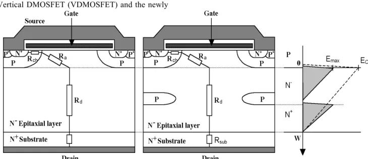
important parameters to be considered. Actually, to reduce the conduction losses in a MOSFET, its specific on-resistance must be reduced. The Vertical Double diffused MOSFET structure — VDMOSFET — (Fig. 1) is widely used as a power MOSFET. This structure is based upon the double diffusion of the P-body and N+ source regions using the edge of the polysilicon as a masking boundary. The voltage handling capability of this structure is given by the breakdown voltage of the “P-body/N-epilayer” junction, that is strongly dependent on the thickness and the doping of the
lower doped region (i.e. the N-epilayer region in the case of N-channel VDMOS transistors) [1].
Today, advances in process technology have improved transistor’s packing density and consequently transistor’s specific on-resistance. However improvements in specific on-resistance have been limited by material and breakdown voltage, which required a relative thick and lowly doped epitaxial layer. Recently, several MOSFET configurations have been proposed to reduce specific on-resistance while keeping a high breakdown voltage: P Floating Islands devices [2], [3], [4] and Superjunction devices [5].
P FLoating Islands unipolar devices — FLIMOSFET [2], Opposite Doped Buried Regions (ODBR) MOSFET [3] and P-buried layer Schottky Barrier Diode [4] — have recently caught the attention of many researchers because they are good challengers of Superjunction devices under 600 Volts [2]; furthermore, the technology needed to manufacture such as devices is less complex than the Superjunction devices technology [4].
In this paper, new Vertical N-channel
FLIMOSFETs dedicated to automotive
applications (12 V / 42 V dual batteries, i.e. below 100 V breakdown voltage devices) are proposed; these FLIMOSFETs comprise only one Pfloating island between drain and source: it will be shown that, even in low voltage applications, they exhibit a better ”specific on-resistance / voltage handling
capability” trade-off than the conventional Vertical DMOSFETs. Then, the “Floating Island” concept will be experimentally validated by the realization of a Floating Island Diode (FLIDiode).
FLOATING ISLANDS MOS PRINCIPLE Principle.
Schematic cross-sections of the conventional Vertical DMOSFET (VDMOSFET) and the newly
developed Vertical FLIMOSFET are shown in Fig. 1 and 2. The essential difference is the introduction of a P buried layer (called FLoating Island) in the N- epitaxial layer; this P buried layer is located under the PHV/N- plane junction in order to divide, under reverse bias conditions, the maximal electric field in two parts (Fig. 3), allowing the improvement of the breakdown voltage for the same N- epitaxial layer doping concentration.
In other words, to reach the same blocking voltage as with a conventional VDMOSFET, the N- epitaxial layer doping concentration of the FLIMOSFET can be strongly increased.
Device parameters.
For instance, when the voltage handling capability of the two devices is about 85 V, the N -epitaxial layer doping concentration required is equal to 5.5 x 1015 cm-3 for the conventional VDMOSFET and to 1.1 x 1016 cm-3 for the FLIMOSFET. Conventional VDiode Vertical FLIDiode central cell Vertical FLIDiode edge cell N- epitaxial layer thickness (µm) 4.75 4.05 4.05 N- Epitaxial layer resistivity (Ω.cm) 1.05 0.50 0.50 Floating P maximum doping concentration (cm-3) -- 10 17 1017 Lateral Floating P maximum doping concentration (cm-3) -- -- 1019
Table 1: Main device parameters of the conventional 91 Volts Diode and the Vertical 95 Volts FLIDiode.
RESULTS AND DISCUSSION
In order to validate the “Floating Island” concept, it has been decided to study and to realize a FLIDiode. This study concerns the reverse behavior of the FLIDiode compared to a conventional PN-N+ Diode. The main device parameters of the two Diodes are given in Table 1. Compared to the conventional Diode, the main
difference is the introduction of a P buried layer in the N- epitaxial layer.
Concerning the OFF-state, it should be noted that 2D simulations confirm what we expected (Fig. 4): the maximal electric field is divided in two parts located around the two junctions (i.e. the body/N-epilayer and the P-buried layer/ N-epilayer junctions); Figure 4 shows the doping concentration (Fig. 4a), electric field distribution (Fig. 4b) and potential distribution
Fig. 1: Conventional Vertical DMOSFET.
Fig. 2: Vertical FLIMOSFET with one FLoating P buried layer between drain and
source.
Fig. 3: Electric field distribution in the conventional VDMOSFET and in
(Fig. 4c) at breakdown in the central cell of the FLIDiode.
(a) (b) (c)
Fig. 4: FLIDiode : Doping concentration (a), Electric field distribution (b), and potential distribution (c) at breakdown.
The schematic cross-section of the edge cell of the FLIDiode is presented Figure 5.
Fig. 5: Edge cell of the Vertical FLIDiode.
In our study, the simulated FLIDiode breakdown voltage of the central cell is about 95 V (Fig. 4c); the breakdown voltage of the edge cell is also 95 V. At breakdown, this structure is in non punch through configuration. The breakdown occurs in the P+N- junction and the electric field is math linear by parts. The electric field is divided by the P+ floating islands. We can also observe that the potential is parabolic by parts, and is sustain by the N- layers. In fact, it can be observed that there is no voltage drop in the P+ floating islands.
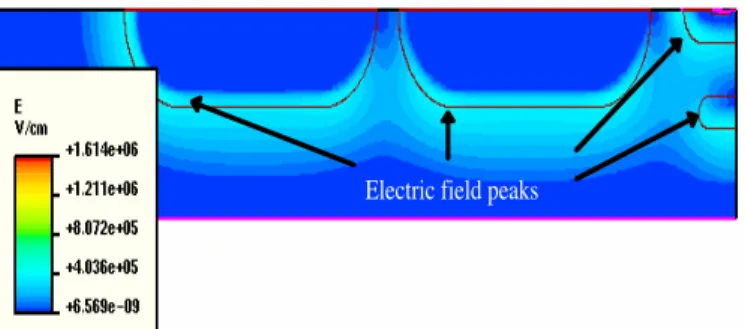
In the edge cell, two lateral P Floating Islands are introduced in the N- epitaxial layer and the positions of the two lateral P FLoating Islands have been optimized: the optimal position is obtained when the maximums of the electric field in the three FLoating Islands and at the PHV cylindrical junction are equal. Figure 6 presents the doping concentration for the edge cell of the Vertical FLIDiode. Figure 7 shows 2D simulation
of the electric field distribution at breakdown for the edge cell of the Vertical FLIDiode. The lateral FLoating Island depth is very important: the more the lateral FLoating Islands are deep, the more the potential lines are pushed away in the volume. Then the breakdown occurs at the PHV plane junction.
Fig. 6: Doping concentration for the edge cell of the Vertical FLIDiode.
Electric field peaks
Fig. 7: Electric field distribution at breakdown for the edge cell of the Vertical FLIDiode.
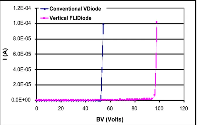
FLIDiodes have been implemented on silicon: Figure 8 shows the variation of the voltage handling capability versus the second epitaxial layer thickness: a wide operating area higher than 85 Volts is obtained.
Fig. 8: BVdss measurements vs 2nd epitaxial layer thickness.
This work validates the FLoating Island concept and the efficiency of the edge cell: this new Diode exhibits an important breakdown
voltage (about 95 Volts) with a N- epitaxial layer doping concentration (1.1 x 1016 cm-3) usually dedicated to 50 V devices.
Figure 9 shows the BVdss measurements of
the conventional Diode (50 Volts) and the Vertical FLIDiode (97 Volts), for the same N- epitaxial layer doping concentration (1.1 x 1016 cm-3).
0.0E+00 2.0E-05 4.0E-05 6.0E-05 8.0E-05 1.0E-04 1.2E-04 0 20 40 60 80 100 120 BV (Volts) I (A) Conventional VDiode Vertical FLIDiode
Fig. 9: BVdss measurements of the conventional Diode and the Vertical FLIDiode.
The Vf measurements presented Figure 10, shows
that the P FLoating Island is fully “transparent”, compared to the conventional Diode (50 Volts) and the Vertical FLIDiode (97 Volts). The P FLoating Island has no impact on the Vf.
1.E-12 1.E-11 1.E-10 1.E-09 1.E-08 1.E-07 1.E-06 1.E-05 1.E-04 1.E-03 1.E-02 1.E-01 1.E+00 0 0.2 0.4 0.6 0.8 1 1.2 V Diode (Volts) I Diode (A) Conventional VDiode Vertical FLIDiode
Fig. 10: Vf measurements of the conventional Diode and the Vertical FLIDiode.
The next step of this work is to implement this concept on Vertical MOSFET: with this high epitaxial layer doping concentration, it can be expected that the specific on-resistance of this new MOSFET will be drastically reduced compared to its equivalent conventional VDMOSFET [5], [6]. This Vertical MOSFET will use the same edge cell as the Vertical FLIDiode. The technology process is now in progress for the FLIMOSFET using more particularly multi-epitaxy layers (see the SUPREM doping profile, Fig. 11). This Vertical MOSFET will use the same edge cell as that of the Vertical FLIDiode.
Fig. 11: SUPREM profile of the new developed FLIDiode. ‘0 µm’ corresponds to the substrate / 1st epitaxial layer interface. ‘- 5.15 µm’ distance corresponds to the surface of the device.
FLIMOSFETs become interesting when increasing the breakdown voltage. For instance, for the same breakdown voltage (about 85 Volts), compared to the conventional VDMOSFET, it has been shown that the specific on-resistance of FLIMOSFET is strongly reduced (33 %) when using P floating squares [6].
CONCLUSION
In this paper, the “FLoating Island” concept has been implemented on silicon, and a FLIDiode has been built for the first time. These experimental results confirm the predictive 2D simulations: this new diode exhibits an important breakdown voltage (about 97 Volts) with a N- epitaxial layer doping concentration (1.1 x 1016 cm-3) usually dedicated to 50 Volts devices. These measurements validate the “FLoating Island” concept and the efficiency of the original edge cell that will be used in the FLIMOS technology: it can be expected that the specific on-resistance of the FLIMOSFET will be drastically reduced compared to the conventional VDMOSFET.
REFERENCES
[1] N. Cézac, F. Morancho, P. Rossel, H. Tranduc, A. Peyre-Lavigne, “A New Generation of Power Unipolar Devices: the Concept of the FLoating Islands MOS Transistor (FLIMOST)”, Proc. ISPSD’2000 (Toulouse, France), pp. 69-72, May 2000.
[2] X.B. Chen, X. Wang, J.K.O. Sin, “A Novel High-Voltage Sustaining Structure with Buried Oppositely Doped regions”, IEEE Trans. On Electron Devices, Vol. 47, n°6, pp. 1280-1285, June 2000. [3] W. Saitoh, I. Omura, K. Tokano, T. Ogura, H. Ohashi, “Ultra Low On-Resistance SBD with P-Buried Floating Layer”, Proc. ISPSD’02 (Santa Fe, USA), pp. 33-36, June 2002.
[4] T. Fujihira, “Theory of Semiconductor Superjunction Devices”, Jpn. J. Appl. Phys., Vol. 36, pp. 6254-6262, 1997.
[5] S. Alves, F. Morancho, J-M. Reynès, B. Lopes, “Vertical N-channel FLIMOSFETs for Future 12 V / 42 V Dual Batteries Automotive Applications”, Proc. ISPSD’2003 (Cambridge, England), pp. 308-311, April 2003.
[6] S. Alves, F. Morancho, J-M. Reynès, B. Lopes, “New Generation of Vertical MOSFETs for Future 12 Volts / 42 Volts Dual Batteries in Automotive Applications”, Proc. EPE’2003 (Toulouse, France), September 2003.