HAL Id: hal-01868496
https://hal.archives-ouvertes.fr/hal-01868496
Submitted on 5 Sep 2018
HAL is a multi-disciplinary open access
archive for the deposit and dissemination of
sci-entific research documents, whether they are
pub-lished or not. The documents may come from
teaching and research institutions in France or
abroad, or from public or private research centers.
L’archive ouverte pluridisciplinaire HAL, est
destinée au dépôt et à la diffusion de documents
scientifiques de niveau recherche, publiés ou non,
émanant des établissements d’enseignement et de
recherche français ou étrangers, des laboratoires
publics ou privés.
Diego Perez-Galacho, Laurent Bramerie, Charles Baudot, Mohamed Chaibi,
Sonia Messaoudene, Nathalie Vulliet, Laurent Vivien, Frederic Boeuf,
Christophe Peucheret, Delphine Marris-Morini
To cite this version:
Diego Perez-Galacho, Laurent Bramerie, Charles Baudot, Mohamed Chaibi, Sonia Messaoudene, et
al.. QPSK Modulation in the O-Band Using a Single Dual-Drive Mach–Zehnder Silicon Modulator.
Journal of Lightwave Technology, Institute of Electrical and Electronics Engineers (IEEE)/Optical
Society of America(OSA), 2018, 36 (18), pp.3935-3940. �10.1109/JLT.2018.2851370�. �hal-01868496�
Abstract— Keeping up with bandwidth requirements in next
generation short- and long-reach optical communication systems will require migrating from simple modulation formats such as on-off keying (OOK) to more advanced formats such as quadrature phase-shift keying (QPSK). In this work, we report the first demonstration of QPSK signal generation in the O-Band using a silicon dual-drive Mach-Zehnder modulator (DD-MZM). The performance of the silicon DD-MZM is assessed at 20 Gb/s and compared against a similar DD-MZM based on LiNbO3,
showing a limited implementation power penalty of only 1.5 dB.
Index Terms— Advanced modulation formats, coherent optical
communications, integrated optics, optical transmitters, silicon modulators, silicon photonics.
I. INTRODUCTION
ILICON photonics devices have shown impressive evolution from the first demonstration of active functions to high-performance transmitters and receivers [1-2]. Interestingly, the use of Si photonics for coherent communications in long haul network could pave the way for future large-scale industrialization of high performance and low cost optoelectronic transceivers [2]. Indeed, while today standards are based on 100-Gb/s transmission, future standards will require 200 or 400-Gb/s transponders, to meet
Manuscript received December XX, 2017; revised January XX, 2018. Published XX, 2018. This work was supported by the European project Plat4m (FP7-2012-318178), the European project Cosmicc (H2020-ICT-27-2015-688516) and the French Industry Ministry Nano2017 program.
L. Vivien and D. Marris-Morini are with the Center for Nanoscience and Nanotechnology, CNRS, Univ. Paris-Sud, Université Paris-Saclay, C2N-Orsay, 91405 Orsay cedex, France (e-mail: laurent.vivien@u-psud.fr; delphine.morini@u-psud.fr).
D. Pérez-Galacho was with the Center for Nanoscience and Nanotechnology, CNRS, Univ. Paris-Sud, Université Paris-Saclay, C2N-Orsay, 91405 Orsay cedex, France. He is now with the ITEAM research institute, Universitat Politècnica de València, Camino de Vera s/n, 46022, Valencia, Spain (e-mail: diepega@upv.es).
L. Bramerie, and C. Peucheret are with Univ Rennes, CNRS, FOTON – UMR 6082, F-22305 Lannion, France (e-mail: laurent.bramerie@enssat.fr; christophe.peucheret@univ-rennes1.fr).
M. Chaibi was with Univ Rennes, CNRS, FOTON – UMR 6082, F-22305 Lannion, France. He is now with Center for Nanoscience and Nanotechnology, CNRS, Univ. Paris-Sud, Université Paris-Saclay, C2N-Orsay, 91405 Orsay cedex, France (e-mail: mohamed.chaibi@c2n.upsaclay.fr).
C. Baudot, S. Messaoudène, N. Vulliet and F. Boeuf are with STMicroelectronics, 850 rue Jean Monnet, 38920 Crolles, France (e-mail: charels.baudot@st.com; sonia.messaoudene-ext@st.com; nathalie.vulliet@st.com; frederic.boeuf@st.com).
with the ever-growing demand triggered by multi-media and cloud-based applications [3]. State-of-the-art silicon on-off keying (OOK) modulators are currently reaching 50-Gb/s operation, [4-5], while higher modulation format such as
n-level pulse amplitude modulation (PAM-n), quadrature
phase-shift keying (QPSK), or 16-state quadrature amplitude modulation (16-QAM) allow to increase transmission rate up to 224 Gb/s [6-12]. As a major step forward, the phase efficiency of the modulators has recently been significantly increased [13-14]. While most of the reported work has been done in the C-band of telecommunication (around 1550 nm), silicon photonics systems are highly attractive for short-distance intra-data-center communications [15], where the O-band (around 1300 nm) is widely used. Despite the lower free-carrier dispersion effect at this wavelength in comparison with 1550 nm, high-performance devices have been demonstrated, showing 50-Gbit/s OOK modulation [16] or low-voltage operation [17]. As the volume of data exchanged inside data centers is continuously increasing, even higher data rates are still required. Developing higher-order modulation formats in the O-band of communications has thus recently received significant attention. 56-Gb/s PAM-4 [18], 112-Gb/s PAM-8 [9] and 200-Gb/s QAM-16 [19] were thus demonstrated.
While standard IQ modulators used for QPSK signal generation are based on nested Mach-Zehnder (MZ) modulator structures [6], a single dual-drive Mach-Zehnder modulator (DD-MZM) has been proposed as a simpler structure, allowing a reduction of the power consumption of the transceiver to generate the QPSK constellation [20]. This scheme has already been demonstrated using a LiNbO3 modulator [21]. Interestingly, this structure offers a better power efficiency and scalability in term of modulation format order that are key advantages for short-distance intra-data-center communications. In this context, we report the first demonstration of QPSK signal generation using a single dual-drive Mach-Zehnder silicon modulator operating in the O-band. As a first demonstration, 20-Gb/s operation is shown, with a large potential for increasing the data rate. Preliminary results of this work have been recently reported in [22]. They are here complemented by a more thorough experimental characterization of QPSK modulation at 10 Gbaud.
QPSK modulation in the O-band using a single
dual-drive Mach-Zehnder silicon modulator
Diego Pérez-Galacho, Laurent Bramerie, Charles Baudot, Mohamed Chaibi, Sonia Messaoudène,
Nathalie Vulliet, Laurent Vivien, Frederic Boeuf, Christophe Peucheret, and Delphine Marris-Morini
based on carrier depletion, using a PN diode embedded in the core of a silicon-on-insulator (SOI) waveguide. The cross section of the phase shifter and its SEM image are reported in Fig 1 (a) and (b), respectively. The rib waveguide is 300-nm high and 400-nm wide. A 50-nm slab is used and provides electrical connection to the highly doped part of the diode. Free-carrier concentration variation is obtained in the core of the waveguide. The PN junction interface is slightly shifted (25 nm) from the center of the waveguide to take benefit from the larger refractive index variation obtained by varying the concentration of holes in comparison with electrons [23]. The targeted doping concentrations are P = 5×1017 cm−3 and N = 1.4×1018 cm−3. Previous work based on the same phase-shifter design allowed demonstrating high modulation efficiency with VπLπ products of 0.95 to 1.15 Vcm for reverse bias from 1 to 4 V at 1310 nm wavelength [17].
The DD-MZM is schematically reported in Fig 1 (c). 2-mm long phase-shifters are embedded in both arms of a symmetric Mach-Zehnder structure. MMI couplers are used as input/output splitter and combiner. Metallic heaters form low-speed/high-efficiency static phase-shifters that are used to bias the interferometer by tuning the DC phase-shift Φ between both arms, as reported in Fig 1 (d). The modulator was fabricated using the 300-mm DAPHNE technological platform from STMicroelectronics [24]. The on-chip losses of the modulator are estimated below 3.8 dB, corresponding to 2.6 dB for the 2-mm-long active region, while losses below
using GSGSG coplanar waveguides.
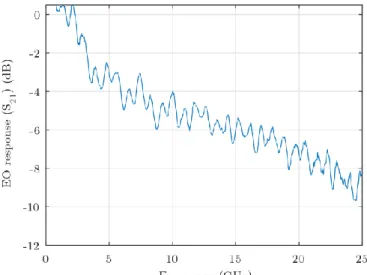
The device bandwidth has been characterized by applying an RF signal to one arm of the modulator, the obtained electro-optical response is shown in Fig. 2. It can be seen that the 3dB electro-optical bandwidth is 5 GHz, while the 6-dB bandwidth is 15 GHz. In comparison the RC cut-off frequency was estimated to be 21 GHz [17]. This result indicates that the electrical/optical signal velocity matching and impedance matching could be further improved. Due to this limitation we decided to focus the QPSK operation at 10 Gbaud. However, this device has the potential to operate at higher speeds of 25 Gbaud, either by improving the RF electrode design, or by
slightly reducing the phase-shifter length, which would increase the bandwidth, at the expense of a reduction of the phase shift per applied voltage.
III. EXPERIMENTAL SET-UP AND QPSK GENERATION
To generate a QPSK signal with a single DD-MZM [20], two independent binary modulating signals are applied to each of the phase-shifters in order to achieve a peak-to-peak phase modulation of π in each arm. At the same time, the phase-shift introduced by the heater is adjusted to operate the DD-MZM in the quadrature point (Φ=π/2). Compared to conventional QPSK transmitters based on IQ modulator architecture, the DD-MZM only required one constant phase-shift and a π phase modulation, hence an applied voltage of V, for each phase-shifter. On the other hand, the IQ modulator requires three constant phase-shifts, two for biasing the two MZMs to the null transmission point and another to set the phase between the two MZMs to quadrature. Furthermore, the IQ modulator requires peak-to-peak voltage differences of 2V to be applied to each nested MZM in order to implement the required π phase modulation. This in turns requires peak-to-peak voltages of V to be applied to the four phase-shifters for proper push-pull operation. Differential logic (data and inverted data) electrical data signals with proper timing
Fig. 1. Cross section of the silicon phase-shifter: (a) schematic and (b) SEM image. Architecture of a DD-MZM: (a) schematic and (b) actual layout.
Fig. 2. Normalized small signal electro-optical response as a function of the applied frequency.
alignment are also required. Finally, it can be noted that in the case of the DD-MZM, an applied peak-to-peak voltage below V will affect the shape of the constellation diagram while in the case of the IQ modulator, a reduced peak-to-peak voltage will be responsible for an increase of the optical loss. Theoretical QPSK eye and constellation diagrams obtained with IQ and DD-MZM modulators are represented in Fig. 3(a) and (b), respectively. It can be seen that the signal generated by the DD-MZM exhibits more intensity ripples than that of the IQ modulator, which are linked to symbol transitions. The areas where the intensity is constant, and which are therefore suited for sampling and phase recovery are represented in grey in the eye diagrams of Fig. 3. It can be seen how the temporal opening of the signal generated by the DD-MZM is reduced compared to the signal generated by the IQ modulator, making the DD-MZM more sensitive to symbol transitions. However, these drawbacks are compensated by a very much simpler hardware architecture and reduced driving voltages.
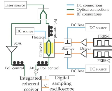
The experimental set-up used for QPSK modulation characterization is reported in Fig. 4. TE-polarized light from an O-band external cavity laser followed by a fiber polarization controller is coupled to the photonic integrated circuit using a single-polarization grating coupler (GC) with typical transmission around -6 dB. The same GC is used to couple the light out of the photonic circuit. Total fiber-to-fiber losses, including coupling and on-chip losses, are thus estimated around 17 dB. The laser source output power was kept to 14 dBm for all the experiments. Two 215−1 long de-correlated pseudo random binary sequences (PRBSs) at 10 Gb/s are used and amplified to reach a swing voltage Vpp of 7 V with DC bias of 4V. GSGSG probes were used at the input to apply the RF signals and at the output of the coplanar waveguide to connect 50-ohm terminations. DC tips were used to connect the heater and adjust the constant phase shift to bias the interferometer at a quadrature point (Φ=π/2). The modulated optical signal is then sent to a coherent receiver
through a variable optical attenuator in order to adjust the received power. For the purpose of this first demonstration, the same laser was used at the transmitter and as local oscillator (LO) at the receiver, thus implementing homodyne detection. A semiconductor optical amplifier (SOA) was used to amplify the LO signal. The I/Q signals of the receiver were fed to a 40-GSps digital sampling oscilloscope (DOS) with 16-GHz electrical bandwidth. Blocks of 105 symbols were acquired and then processed offline. An adaptive finite impulse response (FIR) filter with decision-directed least mean square (DD-LMS) tracking was used as digital signal processing. The processed samples were used to obtain the constellation diagrams and to compute the bit-error-rate (BER). The BER was evaluated over five blocks of 105 symbols.
IV. RESULTS AND DISCUSSION
High-speed measurements of the DD-MZM silicon modulator were performed using the described setup. In order to benchmark its performance, the same characterizations were also performed with a commercial 28-GHz LiNbO3 DD-MZM as well as a 25-GHz LiNbO3 IQ modulator.
The raw received constellation diagrams of the 20 Gb/s QPSK signals generated with the three modulators are represented on the left column of Fig.5. The raw constellation diagram of the signal generated by the silicon DD-MZM is shown in Fig. 5 (a), whereas Fig. 5 (b) and (c) correspond to LiNbO3 DD-MZM and IQ modulator, respectively. The constellations were obtained for a receiver input power of -22 dBm from 20000 samples after resampling, decimation to the baud rate, but without digital equalization. Four group of samples can be observed, which correspond to the four phase states of the QPSK signal. The particular shape of the constellations generated by the silicon and LiNbO3 DD-MZMs is due to the inherent trajectories in the complex plane between the four modulation states, which result in intensity ripples between consecutive symbols, in QPSK generation based on DD-MZMs. Therefore, the measured raw
Fig. 3. Eye and constellation diagrams of a QPSK signal generated with (a) an IQ modulator and (b) a DD-MZM.
Fig. 4. Experimental set-up for QPSK operation of the DD-MZM.
constellation diagrams have the expected shape predicted in Fig. 3 (b). Furthermore, the electro-optical bandwidth limitation of the silicon modulator is responsible for further fluctuations since the phase-shifters directly map residual voltage fluctuations to phase fluctuations. Thanks to its less complicated trajectories of symbol transitions, the raw constellation diagram obtained with the IQ modulator is cleaner. After DSP, classical QPSK constellation diagrams were obtained in the three cases, as represented in the right-side column of Fig. 5. The measured error vector magnitude (EVM) was 18% for the LiNbO3 IQ modulator, whereas for the silicon and LiNbO3 DD-MZMs, EVMs of 33% and 28% were obtained, respectively. The small EVM degradation observed in the silicon DD-MZM with respect to its LiNbO3 counterpart is related to intensity ripples induced by its lower electro optical bandwidth (15-GHz) compared to the LiNbO3 modulator (28-GHz) and by the intensity modulation associated to the free-carrier dispersion effect.
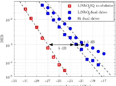
The measured BER performance of the three modulators is shown in Fig. 6 as a function of the receiver input power. It can be seen that a penalty of 5 dB occurs between the LiNbO3 IQ modulator and the LiNbO3 DD-MZM for a BER of 10-3. This power penalty is linked to the presence of intensity ripples that are inherent to this generation scheme, as explained previously. The silicon DD-MZM presents an outstanding low 1.5-dB extra penalty with respect to its LiNbO3 counterpart. This power penalty, as explained previously, is linked to the lower electro optical bandwidth of the silicon DD-MZM with respect to the LiNbO3 and to the
small intensity modulation present on the silicon DD-MZM. V. CONCLUSIONS
We have reported the first use of a silicon DD-MZM to generate QPSK signals in the O-band. This modulation scheme has been evaluated first on a LiNbO3 dual-drive modulator. A power penalty of 5 dB is obtained when compared with standard IQ modulation, linked to the presence of intensity ripples when generating the signal. Interestingly the additional power penalty when using the silicon dual-drive modulator is only 1.5 dB, due to a reduced electro-optical bandwidth of the tested device in comparison with the LiNbO3 modulator. Such penalty could be further decreased thanks to pre-emphasis of the electrical drive voltages or with an optical pulse carver [21,25]. Future works will be focused on improvement of the RF design to exceed the 6-dB electro-optical bandwidth of 15-GHz. 25-Gbaud (i.e. 50-Gb/s) QPSK modulation can thus be expected in the short term.
As a main advantage, this modulator scheme allows using only a single Mach-Zehnder interferometer, with 2×Vπ peak-to-peak voltage instead of 4×Vπ in a standard IQ modulator. Such reduction of the global power consumption to generate the QPSK signal, can be a key advantage for future short distance applications.
REFERENCES
[1] F. Boeuf, S. Cremer, E. Temporiti, M. Fere, M. Shaw, C. Baudot, N. Vulliet, T. Pinguet, A. Mekis, G. Masini, H. Petiton, P. Le Maitre, M. Traldi and L. Maggi, “Silicon Photonics R&D and manufacturing on 300-nm wafer platform,” J. Lightw. Technol., vol. 34, no. 2, pp. 286-295, 2016.
[2] P. Dong, Y.-K. Chen, G.-H. Duan and D. T. Neilson, “Silicon photonic devices and integrated circuits,” Nanophotonics, vol. 3, no. 4-5, pp. 215-228, 2014.
[3] J. Witzens, “Modulators make efficiency leap,” Nat. Photonics, vol. 11, pp. 459, 2017.
[4] P. Dong, L. Chen and Y.-K. Chen, “High-speed low-voltage single-drive push-pull silicon Mach-Zehnder modulators,” Opt. Express, vol. 20, no. 6, pp. 1094-4087, 2012.
[5] D. J. Thomson, F. Y. Gardes, J. M. Fedeli, S. Zlatanovic, Y. Hu, B. P. P. Kuo, E. Myslivets, N. Alic, S. Radic, G. Z. Mashanovich, G. T. Reed, Fig. 5. QPSK constellation diagrams at 10 Gbaud after and before DSP for
(a) silicon DD MZM, (b) LiNbO3 DD-MZM and (c) LiNbO3 IQ modulator (Prx = -22 dBm).
Fig. 6. Measured BER as a function of the average received power for QPSK signal generation.
“50-Gb/s Silicon Optical Modulator,” IEEE Photon. Technol. Lett., vol.
24, no. 4, pp. 234-236, 2012.
[6] P. Dong, C. Xie, L. Chen, L. L. Buhl and Y.-K. Chen, “112-Gb/s monolithic PDM-QPSK modulator in silicon,” Opt. Express, vol. 20, no. 26, pp. B624-B629, 2012.
[7] P. Dong, X. Liu, C. Sethumadhavan, L. L. Buhl, R. Aroca, Y. Baeyens and Y.-K. Chen, “224-Gb/s monolithic PDM-16-QAM modulator and receiver based on silicon photonic integrated circuits,” in Optical Fiber
Communication Conference/National Fiber Optic Engineers Conference 2013, pp. PDP5C.6.
[8] J. Ding, S. Shao, L. Zhang, X. Fu and L. Yang, “Silicon 16-QAM optical modulator driven by four binary electrical signals,” Opt. Lett., vol. 42, no. 8, pp. 1636-1639, 2017.
[9] M. Chagnon, M. Osman, M. Poulin, C. Latrasse, J.-F. Gagne, Y. Painchaud, C. Paquet, S. Lessard and D. Plant, “Experimental study of 112-Gb/s short reach transmission employing PAM formats and SiP intensity modulator at 1.3µm,” Opt. Express, vol. 22, no. 17, pp. 21018-21036, 2014.
[10] A. Samani, D. Patel, M. Chagnon, E. El-Fiky, R. Li, M. Jacques, N. Abadia, V. Veerasubramanian and D. V. Plant, “Experimental parametric study of 128 Gb/s PAM-4 transmission system using a multielectrode silicon photonic Mach Zehnder modulator,” Opt.
Express, vol. 25, no. 12, pp. 13252-13262, 2017.
[11] B. Milivojevic, S. Wiese, C. Raabe, A. Shastri, M. Webster, P. Metz, B. Chattin, B. Dama and K. Shastri, “Small-Size Silicon Photonic IQ Modulator and Low-Power CMOS Driver for Next Generation Coherent Transceiver,” in 18th European Conference on Network and Optical
Communications & 8th Conference on Optical Cabling and Infrastructure, 2013, pp. 181-184.
[12] A. Shastri, C. Muzio, M. Webster, G. Jeans, P. Metz, S. Sunder, B. Chattin, B. Dama and K Shastri, “Ultra-Low-Power Single-Polarization QAM-16 Generation Without DAC Using a CMOS Photonics Based Segmented Modulator,” J. Lightw. Technol., vol. 33, no. 26, pp. 1255-1260, 2015.
[13] T. Hiraki, T. Aihara, K. Hasebe, K. Takeda, T. Fujii, T. Kakitsuka, T. Tsuchizawa, H. Fukuda and S. Matsuo, “Heterogeneously integrated III-V/Si MOS capacitor Mach-Zehnder modulator,” Nat. Photonics, vol. 11, no. 8, pp. 482, 2017.
[14] J.-H. Han, F. Boeuf, J. Fujikata, S. Takahashi, S. Takagi and M. Takenaka, “Efficient low-loss InGaAsP/Si hybrid MOS optical modulator,” Nat. Photonics, vol. 11, no. 8, pp. 486, 2017.
[15] T. Pinguet, B. Analui, E. Balmater, D. Guckenberger, M. Harrison. R. Koumans, D. Kurcharski, Y. Liang, G. Masini, A. Mekis, S. Mirsaidi, A. Narasimha, M. Peterson, D. Rines, V. Sadagopan, S. Sahni, T. J. Sleboda, D. Song, Y. Wang, B. Welch, J. Wtizens, J. Yao, S. Abdalla, S. Gloeckner, P. De Dobbelaere and G. Capellini, “Monolithically integrated high-speed CMOS photonic transceivers,” in 5th IEEE
International Conference on Group IV Photonics, 2008, pp. 362-364. [16] M. Streshinsky, R. Ding, Y. Liu, A. Novack, Y. Yang, Y. Ma, X. Tu, E.
K. S. Chee, A. E.-J. Lim, P. G.-Q. Lo, T. Baehr-Jones and M. Hochberg, “Low power 50 Gb/s silicon traveling wave Mach-Zehnder modulator near 1300nm,” Opt. Express, vol. 21, no. 25, pp. 30350-30357, 2013. [17] D. Perez-Galacho, C. Baudot, T Hirtzlin, S. Messaoudene, N. Vulliet, P.
Crozat, F. Boeuf, L. Vivien and D. Marris-Morini, “Low voltage 25Gbps silicon Mach-Zehnder modulator in the O-band,” Opt. Express, vol. 25, no. 10, pp. 11217-11222, 2017.
[18] C. Xiong, D. M. Gill, J. E. Proesel, J. S. Orcutt, W. Haensch and W. M. J. Green, “Monolithic 56Gb/s silicon photonic pulse-amplitude modulation transmitter,” Optica, vol. 3, no. 10, pp. 1060-1065, 2016. [19] C. R. Doerr, L. Chen, T. Nielsen, R. Aroca, L. Chen, M. Banaee, S.
Azemati, G. McBrien, S. Y. Park, J. Geyer, B. Guan, B. Mikkelsen, C. Rasmussen, M. Givhechi, Z. Wang, B. Potsaid, H.-C. Lee, E. Swanson and J. Fujimoto, “O, E, S, C and L Band Silicon Photonics Coherent Modulator/Receiver,” in Optical Fiber Communication Conference
Postdeadline Papers 2016, pp. Th5C.4.
[20] K.-P. Ho and H.-W. Cuei, “Generation of Arbitrary Quadrature Signals Using One Dual-Drive Modulator,” J. Lightw. Technol., vol. 23, no. 2, pp. 764-770, 2005.
[21] D. Krause, J. C. Cartledge and K. Roberts, “Demonstration of 20-Gb/s DQPSK With a Single Dual-Drive Mach-Zehnder Modulator,” IEEE
Photon. Technol. Lett., vol. 20, no. 6, pp. 1363-1365, 2008.
[22] L. Bramerie, D. Perez-Galacho, C. Baudot, M. Chaibi, S. Messaoudene, N. Vulliet, L. Vivien, D. Marris-Morini, C. Peucheret, “20 Gbps QPSK Signal Generation using a Silicon Dual-Drive Mach-Zehnder Modulator
Operating in the O-Band,” in 43rd European Conference on Optical
Communication, 2017, pp. Th1C.2.
[23] R. Soref and B. R. Bennett, “Electrooptical effects in silicon,” IEEE J.
Quantum Electron., vol. 23, no. 1, pp. 123-129, 1987.
[24] C. Baudot, A. Fincato, D. Fowler, D. Perez-Galacho, A. Souhaite, S. Messaoudene, R. Blanc, C. Richard, J. Planchot, C. De-Buttet, B. Orlando, F. Gays, C. Mezzomo, E. Bernard, D. Marris-Morini, L. Vivien, C. Kopp and F. Boeuf, “Daphne silicon photonics technological platform for research and development on wdm applications,” in Proc.
SPIE 9891, 2016, pp. 98911D.
[25] W.-R. Peng, J. Chen, S. Y. Tsai, C. Tsao and S. Chi, “Evaluation of the inherent ripple effects on the performance of an optical DQPSK signal generated by using only one MZM,” in International Conference on
Photonics in Switching, 2006, pp. 1-3.
Diego Pérez Galacho received the MSc in
Telecommunication Engineering from Málaga University (Spain) in 2011. From 2011 until September 2013, he was working in the design of coherent receivers in III-V technology at the Photonics & RF research laboratory at Málaga University. In September 2013, he joined the Silicon Photonics research group at Paris-Sud University, where he worked on the development of silicon transceivers. In October 2016, he defended his PhD entitled “High speed optical modulation, advanced modulation formats and mode division multiplexing in Silicon Photonics” at Paris-Sud University. Since October 2017 he works in the Photonics Research Labs at Polytechnic University of Valencia developing optical links with Spatial Division Multiplexing for fronthaul mobile networks. His research interests comprise devices based on periodic structures and analog and digital optical communication systems including polarization diversity and space division multiplexing.
Laurent Bramerie biography not available at the time of
publication
Charles Baudot (Senior Member, IEEE) obtained his MSc
degree in microelectronics form Université Pierre et Marie Curie, Paris, France in 2004 and his PhD degree from Nanyang Technological University, Singapore in 2010. He joined STMicroelectronics in Singapore in 2005 as an R&D engineer to explore alternative technologies to silicon. In the course of that activity he worked on molecular electronics, carbon nanotube based electronics and printed electronics. In 2010 he moved to STMicroelectronics, France as an advanced R&D senior staff engineer where his activity is devoted to the development of advanced silicon photonic device and process integration.
Mohamed Chaibi biography not available at the time of
publication
Sonia Messaoudène received her Diploma of Higher
2009 she worked at Tronics, Crolles (France) on electrical and dynamic sensor testing. She currently works as a process integration technician at STMicroelectronics, Crolles (France) on the follow up of advanced silicon photonics process R&D.
Nathalie Vulliet received her M.Sc. degree in 1996 from INP
Grenoble, France. In 1989, she joined Thomson Semiconductors, Grenoble and worked on the electrical characterization of CMOS and BICMOS process development during 4 years. She was then involved in the reliability analysis of advanced CMOS technologies with SGS–Thomson Microelectronics (currently STMicroelectronics), Central R&D, Crolles, France. In 2002, she joined the Advanced Devices team to be involved in the collaborative R&D between STMicroelectronics and CEA–LETI working on the process development of multichannel advanced MOSFET. In 2011, she joined the Advanced Device Technologies team of the Silicon Technology Development department and since then she works on the process integration of silicon photonic technologies in the 300mm Crolles wafer foundry.
Laurent Vivien received the Ph.D. degree in physics from the
Polytechnique School, Palaiseau Cedex, France, in 2001. His Ph.D. Thesis was on nonlinear optical properties of carbon nanotubes for optical limiting.Between 2001 and 2003, he held a postdoctoral position with the Institute of Fundamental Electronics (IEF), Orsay, France, where studied single-mode and polarization-insensitive structures in silicon-on-insulators and the coupling from sub-micrometric waveguides to single mode fiber for optical telecommunication applications. Since 2003 he has joined the CNRS at the Institute of Fundamental Electronics where his activities are related to passive (waveguide, splitters, 90° turns, optical couplers) and active
interconnects and optical fiber communications.
Frederic Boeuf biography not available at the time of
publication
Christophe Peucheret received the graduate engineering
degree from Telecom Bretagne, Brest, France, the M.Sc. degree in microwaves and optoelectronics from University College London, London, U.K., and the Ph.D. degree from the Technical University of Denmark (DTU), Copenhagen, Denmark. He has been with the Department of Photonics Engineering at the Technical University of Denmark between 1997 and 2013. Since September 2013 he is with the FOTON Institute (Univ. Rennes, CNRS - UMR 6082), Lannion, France. His current research interests include the applications of silicon photonic devices to optical communication systems and interconnects.
Delphine Marris-Morini received her PhD from the
University of Paris Sud in 2004 on the development of high speed silicon modulators. She is now a Professor at Paris Sud University and she is also a junior member of the Institut Universitaire de France (IUF) since 2013. Her research interest includes efficient and high speed optoelectronic devices for silicon photonics. Recently she received an ERC starting grant (INsPIRE) on mid-IR photonics chips. She received the bronze medal from CNRS in 2013. She has published over 70 journal papers. She is in charge of the group of Micro and Nanophotonic devices on silicon since 2015.