T
T
H
H
È
È
S
S
E
E
En vue de l'obtention du
D
D
O
O
C
C
T
T
O
O
R
R
A
A
T
T
D
D
E
E
L
L
’
’
U
U
N
N
I
I
V
V
E
E
R
R
S
S
I
I
T
T
É
É
D
D
E
E
T
T
O
O
U
U
L
L
O
O
U
U
S
S
E
E
Délivré par l'Université Toulouse III - Paul Sabatier
Discipline ou spécialité : NANO-PHYSIQUE.
JURY
Louis PORTE, Professeur à l’Université Paul Cézanne Aix-Marseille III. William SACKS, Professeur à l’Université Pierre et Marie Curie Paris VI. Roland CORATGER, Professeur à l’Université Paul Sabatier à Toulouse.
Tomaso Zambelli, Habilité à Diriger des Recherches à l’Institut f. Biomedizinische Technik, Zurich.
Jacques VIGUÉ, Directeur de recherche CNRS à l'Université Paul Sabatier à Toulouse. Sébastien GAUTHIER, Directeur de recherche CEMES-CNRS à Toulouse.
Ecole doctorale : Sciences de la Matière
Unité de recherche : Centre d’Elaboration de Matériaux et d’Etudes Structurales (CEMES),
UPR 8011 CNRS
Directeur(s) de Thèse : Sébastien GAUTHIER
Rapporteurs : Louis PORTE et William SACKS
Présentée et soutenue par Miguel Angel VENEGAS DE LA CERDA
Le 30 Septembre 2008
Titre : Etudes expérimentales de surfaces et de films minces isolants par microscopie à sonde locale sous ultra vide
ECOLE DOCTORALE
SCIENCES DE LA MATIERE
DOCTORAT DE L’UNIVERSITE DE TOULOUSE III - Paul Sabatier. Discipline : NANO-PHYSIQUE, NANO-COMPOSANT,
NANO-MESURE.
Miguel Angel VENEGAS DE LA CERDA.
Etudes expérimentales de surfaces et de films minces isolants par
microscopie à sonde locale sous ultra vide
Thèse dirigée par Sébastien GAUTHIER
Date de la soutenance, le 30 Septembre 2008
Jury :
Louis PORTE, Professeur à l’Université Paul Cézanne Aix-Marseille III, IM2NP/ L2MP-Marseille, Rapporteur.
William SACKS, Professeur à l’Université Pierre et Marie Curie Paris VI, INSP/STMSG- Paris, Rapporteur.
Roland CORATGER, Professeur à l’Université Paul Sabatier, CEMES/GNS-Toulouse.
Tomaso Zambelli, Habilité à Diriger des Recherches à l’Institut f. Biomedizinische Technik, ETH-Zurich, Switzerland.
Jacques VIGUÉ, Directeur de recherche CNRS, IRSAMC/LCAR-Toulouse.
Sébastien GAUTHIER, Directeur de recherche CNRS, CEMES/GNS-Toulouse.
Dans ce travail de recherche nous avons réalisé des études expérimentales de surfaces et de films minces isolants par microscopie à sonde locale sous ultra vide à température ambiante. En particulier nous avons utilisé la microscopie à effet tunnel (STM) et la microscopie à force atomique en mode non-contact (NC-AFM). Nous présentons des résultats qui concernent deux systèmes : la surface isolante KBr(001) et le film mince isolant d'alumine formé par oxydation de la surface (110) d'un cristal de NiAl.
• Dans un premier temps, nous avons modifié la tête du microscope STM/AFM en changeant le dispositif de détection optique des oscillations du cantilever. L'amélioration importante apportée nous a permis de mener une série d'expériences sur la surface de clivage du cristal ionique KBr(001). Nous avons mis en évidence à partir d'images de marches monoatomiques acquises avec la résolution atomique des changements de contraste réversibles déclenchés par le passage de la pointe sur le bord de marche. Ces observations ont été interprétées en terme de déplacements atomiques à l'extrême apex de la pointe entraînant un changement de signe de l'ion terminal, qui détermine le type d'image observée. Cette hypothèse a été confirmée en analysant les courbes expérimentales donnant la force entre la pointe et la surface en fonction de la distance pointe-surface. Cette étude a été suivie de quelques tentatives pour imager des molécules organiques sur cette surface isolante.
• Le système Pd/Al10O13/NiAl(110) à été étudié par microscopie à effet tunnel. La
couche d'oxyde est formée par l'exposition à O2 à une température particulier
(~280°C) de la surface (110) d'un cristal de NiAl sous ultravide. Nous avons obtenu des images en résolution atomique qui nous ont permis de remonter à la structure atomique de la couche isolante d'alumine, de stœchiométrie Al10O13, ainsi que de l'un
des types de parois de domaine du film isolant. Nous avons également réalisé de mesures de façon à caractériser ses propriétés électriques à une échelle nanométrique. Ce substrat nous a ensuite servi à faire croître des agrégats métalliques de palladium dans différentes conditions. La répartition des îlots ainsi formés n'est pas homogène, certains défauts étant décorés par le palladium. La possibilité d'utiliser ce substrat pour réaliser des jonctions métal-molécule-métal planaires connectables à un système de mesure extérieur par la méthode du nano-stencil développée au CEMES a ensuite été envisagée.
Les perspectives ouvertes par ce travail dans le domaine de l'électronique moléculaire sont discutées dans la conclusion du manuscrit.
mots clés : Microscopie à effet tunnel, microscopie à force atomique, mode non-contact,
Exploring bulk insulating surfaces and thin insulating films, at the atomic level by UHV-SPM techniques.
In this research work we carried out experimental studies of insulating surfaces and insulating thin films surfaces by scanning probe microscopy techniques under ultra vacuum at room temperature. In particular we used Scanning Tunneling Microscopy (STM) and Atomic Force Microscopy in the non contact mode (NC-AFM). We present experimental results on two systems: the insulating surface KBr (001) and the thin insulating alumina film formed by oxidation of the (110) surface of a NiAl crystal.
• Initially, we modified the STM/AFM head by changing the optical device of the detection of the cantilever oscillations system. This crucial improvement enabled us to carry out a series of experiments on the (001) cleaved surface of the ionic crystal KBr at the atomic level. We have evidence obtained from atomic resolution images, that shows a change in contrast when the tip passes through a step edge. Where we could observe a systematic and reversible change in the contrasts of the image. These observations were interpreted in terms of the atomic displacements of the last extremity tip apex, involving the change of last ion sign. This change of ion determines the type of image observed at atomic resolution. This assumption was confirmed by analyzing the experimental curves giving the force between the tip and the surface according to the tip to surface distance. This study was followed of some attempts to images organic molecules on this insulating surface.
• The Pd/Al10O13/NiAl (110) system was explored by STM and scanning tunneling
spectroscopy (STS), where the oxide layer is formed by exposing the NiAl(110) surface to an oxygen atmosphere, while keeping the sample temperature at (~280°C) under ultra-high vacuum. The atomic resolution images obtained enabled us to go down into the atomic structure of the insulating alumina layer, with stoichiometry Al10O13. In addition, it could be possible to atomically resolve a unit cell of one type
of defects formed. We also carried out electrical measurements in order to characterize its electric properties on a nanometer scale. This substrate was then used to growth metal palladium aggregates under various conditions. The distribution of the small formed islands is not homogeneous; certain defects of the alumina film are being decorated by palladium aggregates. The possibility to use this substrate to carry out suitable experiment for interconnections of planar junctions involving a metal-molecule-metal junction onto an external measurement system may probably be considered. This can be held by the nano-stencil technique, developed in the GNS at CEMES
Prospects opened by this work in the field of molecular electronics are discussed in the conclusion part of the manuscript.
Keywords : Scanning tunnelling microscopy, atomic force microscopy, non contact mode,
LABORATOIRE DE RATTACHEMENT :
Centre d’Elaboration de Matériaux et d’Etudes Structurales (CEMES),
UPR 8011 CNRS
29 rue Jeanne Marvig (BP 94347)
31055 TOULOUSE Cedex 4 FRANCE
l’état d’Aguascalientes (CONCYTEA) pour tout le soutien qu’il m’a apporté. Grâce à cette
bourse de l’état d’Aguascalientes j’ai eu la possibilité de poursuivre mes études à l’étranger en nanosciences, merci beaucoup.
J’exprime tous mes remerciements aux rapporteurs, Louis PORTE et William SACKS, de s’être intéressé à ces travaux.
J’exprime tous mes remerciements aux membres du jury, Roland CORATGER,
Tomaso ZAMBELLI et Jacques VIGUÉ pour avoir accepté de faire partie du jury et pour avoir
pris de leur temps pour lire cette thèse.
Je voudrais aussi beaucoup remercier M. Jean-Pierre LAUNAY, directeur du Centre
d’Elaboration des Matériaux et d’Etudes Structurales (CEMES), pour m’avoir aidé à tout
moment et pour cette grande opportunité d’avoir fait mon doctorat au CEMES. Je suis très reconnaissant envers Christian JOACHIM pour deux raisons:
Tout d’abord pour sa motivation constante, son énergie transmise, ses conseils, son attention, sa patience, son amitié, et son courage qu’il m’a consacrés avec grande sympathie, toujours et depuis notre rencontre aux États Unis à Nanotech2003. Merci de m’avoir transmis ces éléments clés qui m’ont donné la force de poursuivre mes études dans le domaine fascinant des nano sciences.
En second, car grâce à lui j’ai eu la belle opportunité de venir en France poursuivre mes études dans un des meilleurs groupes de recherche du monde en Nano Sciences, le GNS.
J’exprime toute ma reconnaissance et mes plus sincères remerciements de manière très particulière à mon directeur de thèse, M. Sébastien GAUTHIER. Grâce à sa patience, sa compréhension, son attention, ses orientations, sa motivation, ses conseils, et ses efforts j’ai pu finir cette thèse. Merci à lui qui dans les moments les plus difficiles et critiques de ce travail m’a toujours apporté tout son soutien et son aide. Grâce à ses nombreux enseignements et connaissances, ce travail a acquis la qualité scientifique nécessaire. Merci toujours !
Je remercie spécialement de tout mon amour ma femme Jessy, qui a toujours été avec moi et m’a toujours soutenu dans les moments les plus durs de cette aventure, à qui je dédie tous mes efforts. Ainsi qu’à ma famille pour tout son soutien.
Merci à David MARTROU pour ces apports et conseils partagés pendant la partie expérimentale de cette thèse.
Mille mercis à Haiming GUO pour m’avoir enseigné à travailler l’Ultra Vide d’une façon toujours très sympa et très attentive.
Je remercie également Jose ABAD, « Départamento de Física, Centro de Investigación Optica y Nanofìsica-CIOyN », de l’Université de Murcia en Espagne pour tout ses apports qui ont été d’une grande aide pour les expériences en AFM.
Je dois exprimer mes remerciements les plus sincères à Olivier GUILLEMET pour ses conseils de préparation d’échantillons et déposition de molécules qu’il m’a toujours donnés d’une façon très amicale et sympathique, sa précieuse aide, dans mes études expérimentales en microscopie de champ proche sous ultra vide, a été de grand aide.
Je remercie vivement Jérôme POLESEL pour les petites conversations très enrichissantes, son travail de thèse m’a toujours apporté des éléments indispensables pour la compréhension de la machinerie d’AFM en mode dynamique.
Je dis merci à Henri- Pierre JAQUOT pour ses conseils en chimie qu’il m’a donné toujours avec grande sympathie.
Je remercie à Christophe DESHAYES pour sa précieuse collaboration dans les images en SEM des Cantilevers, et à Théophile Noël pour sa collaboration dans les études préliminaires pour l’implémentation de la Diode super luminescent.
A E. Meyer, L. Nony pour leurs précieuse conseils et orientations pour effectuer le changement du système optique, je les dis merci beaucoup.
Un grand merci à tous ceux qui m’ont accueilli au CEMES ainsi qu’à tout le personnel du laboratoire. Je voudrais remercier dans son ensemble le groupe GNS ainsi que le CEMES pour ce grand accueil et le soutient lors de l’élaboration de ce travail.
Et finalement merci à tout le monde pour les petites aides qu’ils m’ont toujours offertes.
Dedicada a Jessy con todo mi amor:
por todo su gran apoyo, esfuerzo, paciencia,
comprensión y amor.
Que sin su soporte, no hubiéramos sobrevivido en Toulouse.
1. General Introduction 19
1.1. Antecedents: the nano-stencil technique……….………….………19
1.1.1. Molecular electronics………19
1.1.2. Connecting a single molecule……….…..…..…..20
1.1.2.1. The STM metal-vacuum-molecule-substrate junction………...…20
1.1.2.2. Mechanically Breakable Junction……….……...21
1.1.2.3. The CNT–MB–CNT covalent junction approach.……….………….21
1.1.2.4. The 4-ISPM Interconnects approach.………….……...22
1.1.3. The Nanostencil technique………....24
1.2. Contributions of this work………....…27
1.2.1. Non – Contact Atomic Force Microscopy……….…...…27
1.2.1.1. NC-AFM history………...………...27
1.2.1.2. NC-AFM principle……….29
1.2.1.3. Optical beam deflection sensor………...32
2. Optimization of the AFM beam deflection sensor 35
2.1. Introduction………...….35
2.2. Sensitivity of the optical beam method………...….36
2.3. Source of noises………..……38
2.3.1. The shot noise……….………..……39
2.3.2. The Johnson noise………..………...…40
2.3.3. The optical source noise……….…...…40
2.3.3.1. Laser noises………...……….…40
2.3.4. The cantilever thermal noise………..….….….41
2.4. Modifications of the RT AFM Omicron head……….…….………...42
2.4.1. The superluminescent laser diode………...…43
2.4.2. The single mode optical fiber………....…44
2.4.3. The focusing optics……….…..…46
2.4.4. New characteristics of the beam deflection sensor……….…...47
2.5. Noise spectral analysis………...……48
2.5.1. Estimation of the equivalent input noise of the new beam deflection system……….………..52
Contest
2.6. Sensitivity measurement and amplitude calibration………..…54
2.7. Conclusions and perspectives………..………...…..…56
3. NC-AFM study on KBr(001) 59
3.1. Introduction……….……….…..59
3.2. Experimental methods……….……….….60
3.2.1. Force spectroscopy………..……..………..…..61
3.2.1.1.Extraction of the force from ∆f(z) using the Sader-Jarvis formula...61
3.2.1.2.Description of the technique………...64
3.3. Results………...……..……66
3.3.1. Two types of atomic resolution images……….……...………66
3.3.2. Atomically resolved force curves………...…..…………67
3.3.3. Spontaneous tip polarity reversal………...70
3.3.4. Tip polarity reversal on a monoatomic step………...……….…..71
3.3.5. Potential energy surfaces of the two-level system………….……….…….….73
3.3.6. Tip polarity reversal on two successive monoatomic steps.……….74
3.3.7. Discussion of the topography results………..……….….78
3.4. Force spectroscopy with the bistable tip………..………...….…79
3.5. General discussion………..………...82
3.6. Conclusion……….………...84
4. The Pd/Al10O13/NiAl(110) system 87
4.1. Introduction………....…87
4.2. The NiAl(110) intermetallic alloy……….…..…..88
4.2.1. Preparation procedure……….……..……89
4.3. The alumina film formed on NiAl(110)……….………...……90
4.3.1. Preparation procedure……….……..………90
4.3.2. The oxide film meso scale morphology………....……..…….….91
4.3.3. Intermediate scale images………..………...93
4.3.4. Structural relation between the alumina unit cell and the NiAl(110) substrate………..94
4.3.5. Higher Resolution image, with three domain boundaries………….……...….95
4.3.6. Atomic resolution image of the oxide film surface…………...…….……..….97
4.3.8. Interpretation of the atomic resolution image of domain A…....….…………99
4.3.9. The IA-Anti Phase Domain Boundary atomistic model……….………...….100
4.3.10.Interpretation of the atomic resolution image of the IA – APDB…..…..…...101
4.3.11.Meshing the surface with the repetitive pattern………..……101
4.4. Scanning tunneling Spectroscopy measurements………...103
4.4.1. Introduction………...103
4.4.2. Determination of the electronic gap for a 1700 L alumina film………...104
4.4.3. Apparent thickness of the oxide film as a function of the imaging bias voltage……….………...….105
4.4.4. STS measurements in the gap of two different oxides………...…108
4.5. Palladium growth…………..……….……….……110
4.6. Conclusion………..………….…….111
5. Conclusions and perspectives 113
5.1. Conclusions…..……….………113
5.2. Perspectives ………..………….………..……115
5.3. Molecules visualization attempts………..……….…………115
5.3.1.1.Deposition by sublimation under UHV………….………...……115
5.3.1.2.Deposition from a chloroform solution…………...………..116
5.3.2. Nano manipulation………...………...……118
6. References 123
CHAPTER 1
General Introduction
Introduction
This chapter is divided into two parts. The first one is dedicated to introduce the reader into the domain of interest. The different methods that have been recently developed to electrically connect a molecule between electrodes will be shortly discussed. In particular, we will go more into detail in the developments made in the GNS group. We will show some achievements already performed and what are the future goals to be achieved. In the second part of this chapter, we present an overview of how this thesis has contributed to some of the goals exposed in the first part. The experimental results that will be developed all along this thesis are then briefly presented.
1.1 Antecedents: The nano-stencil technique.
1.1.1 Molecular electronics
The constant miniaturization of the electronic components driven by the needs of the microelectronics industry has shown tremendous progress in the construction of smaller and smaller electronic devices. A common component normally used as a building block of an electronic circuit is the transistor, which recently could be considerably reduced in size in the sub-micrometer range, with a gate thickness below 50 nm and limited to 15 nm [Stephen2006]. However, this miniaturization of electronic components is starting to be affected by technological and fundamental limits, from where other miniaturization
Chapter 1 General Introduction
community are being developed in order to propose molecules as new candidates for nano-meter sized building blocks with the goal of integrating them into future electronic components. To achieve this goal, new challenges need to be tackled. In particular, it is required to develop methods to connect single molecules to macroscopic conductive electrodes. In the following, we discuss the most interesting approaches to address a single molecule being explored nowadays.
1.1.2 Connecting a single molecule.
1.1.2.1 The STM metal-vacuum-molecule-substrate junction.
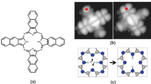
Figure 1.1: LT-STM image showing the switching of a single naphthalocyanine molecule on NaCl/Cu(111) by tunnelling current. From [Liljeroth2007].
The most flexible and easy way to electronically access and to contact a single molecule today in Ultra High Vacuum (UHV) conditions has been rendered possible thanks to the incoming of Scanning Probe Microscopy (SPM) techniques and surface science developments. In particular, Scanning Tunnelling Microscopy (STM) can perform experimental studies of organic molecules deposited on the following substrates: metallic surfaces, insulating films grown on metallic substrates, semiconducting surfaces and/or insulating films on semiconducting substrates. A very nice example can be found in [Liljeroth2007] that shows the experimental study of a single naphthalocyanine molecule (fig. 1.1a) deposited on a NaCl(100) bi-layer previously grown on top of Cu(111). Interestingly, it was found that this molecule displays a two-state behavior due to a tautomerization involving the displacement of two hydrogen atoms from one pair of nitrogen atoms to the other in the central cavity of the molecule (shown in fig. 1.1c). This activation was produced by a tunnelling current injected with the STM tip in the red spot of fig. 1.1b. The corresponding STM images show how these proton transfers affect the LUMO orbital, inducing a transition between a high- and a low
current state. This experiment shows an important progress for novel molecular logic devices with functional molecules. One major drawback of this STM-based approach is that it is limited to two electrodes and the geometry of connection cannot be chosen at will.
1.1.2.2 Mechanically Breakable Junctions.
Figure 1.2: The mechanically breakable junction schematic with (a) the bending beam, (b) the counter supports, (c) the notched gold wire, (d) the glue contacts, (e) the piezo element,
and (f) the glass tube containing the molecular solution.
Another approach described in 1997 by M. Reed and J. Tour [Reed1997], shows an experiment at room temperature with a mechanically controllable break junction (MCB) (Fig. 1.2). In this approach, a notched metal wire is glued onto a flexible substrate and is fractured due to the bending of the substrate by a piezo element. This mechanism can establish an adjustable tunnelling gap. A large reduction factor between the piezo elongation and the electrode separation ensures an inherently stable contact or tunnel junction. The wire contacts are atomically sharp when broken, as demonstrated in the conductance quantization observed on the I(V) characteristics of the junction. In the experiments reported here, benzene-1,4-dithiol molecules were adsorbed from a solution on the surface of the two gold electrodes of the break junction. This results in the formation of a self-assembled monolayer (SAM) on the gold electrodes. Characteristic features, detected on the I(V) characteristics of the junction were attributed to the presence of one or a few molecules positioned between these electrodes. One major drawback of this approach is that it is not possible to image the junction in order to establish its precise structure.
1.1.2.3 The CNT–MB–CNT covalent junction approach.
The idea is to use carbon nanotubes as intermediate electrodes to connect a molecule. Carbon nanotubes have lengths in a range (several thousands of nm) which makes them easy to
Chapter 1 General Introduction
connect to metallic electrodes and diameters (1 to 2 nm) that are close in dimensions to smaller objects, like molecules.
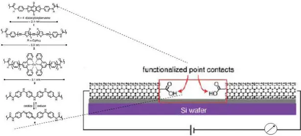
Figure 1.3: A molecular bridge composed of two or three molecules connected between two single wall carbon nanotubes.
In the work reported by Nuckolls and co-workers, single wall carbon nanotubes (SWNT), deposited on a substrate are locally cut by oxidation. This cut produces a 10 nm gap and leaves the terminations of the SWNT with specific ending chemical groups (carboxylic acid groups). These carboxylic acid groups can then create covalent bonds with the oligoaniline type molecules of the solution in which this system is subsequently introduced. These molecules serve as molecular bridge connectors in between the 10 nm gap of the nanotube [Nuckolls2006]. Note that the gap is not small enough to be occupied only by a single molecule but by a bridge of two or three of them, furthermore the precise structure of the junction is not known.
The next approaches have the ambition to avoid the drawbacks of these methods by combining the visualization and manipulation capabilities of STM or AFM with a planar architecture.
1.1.2.4 The 4-ISPM Interconnects approach.
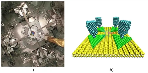
Another strategy currently being developed is based on the facilities provided by the commercial UHV four independent scanning probes microscope (4-ISPM), from Omicron Nanotechnology [Omicron2008a], in combination with recent surface science progress [Yang2007].
The 4-ISPM (figure 1.4a) is integrated in a common stage and equipped with a scanning electron microscope. The entire equipment is a sophisticated analytical instrument, designed for local and non-destructive four point contact for electrical measurements and in situ function tests of mesoscopic devices.
Using the four tips of this device to directly connect a single molecule is not possible, due to the size of the tips. One needs to use intermediate electrodes. An approach based on the manipulation of gold islands on MoS2 was recently proposed [Yang2007]. It is illustrated in
figure 1.4b. Four islands are used to connect a single molecule. It is important that the islands have a small height, to allow STM or AFM imaging in the inter-electrode area. This is the case for the gold islands that are grown on MoS2. In addition, it turns out that these islands
can be manipulated so that the relative position of the four electrodes can be adapted to the molecule to be connected.
This strategy faces two major challenges:
Addressing the islands will require building ultra sharp tips.
Finding metal/substrate systems where the substrate has the desired electronic properties (it should ideally have a large band gap) and the metal grows in a 2D mode to get large islands with a small height is a difficult task because, generally, for thermodynamic reasons, metals tend to grow 3D on these low energy surfaces (note that MoS2 is a
semiconductor, but with a rather low gap of ~1.2 eV [Lauritsen2004]).
a) b)
Figure 1.4: a) The four STM tips stage, with the sample in the center and b) atomistic view of the proposed interconnection.
Chapter 1 General Introduction
The next approach is similar to the present one, except that fixed electrodes are used instead of four mobile STM tips. It develops the idea of using intermediate scale electrodes. For this reason, it suffers from the same limitations concerning the metal/substrate system.
1.1.3 The Nanostencil technique.
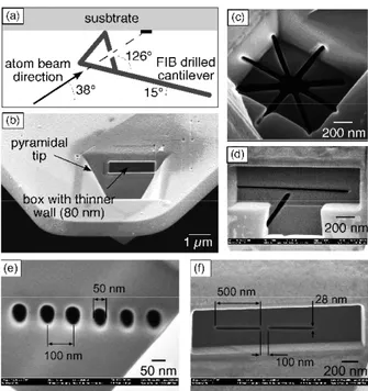
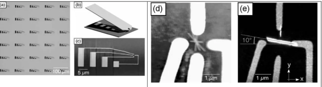
The nanostencil technique consists in using a stencil deposition mask embedded in an AFM cantilever to make nanoelectrodes (figure 1.5a). As shown in figure 1.5b, a membrane is managed in the side of the hollow tip of a cantilever by Focused Ion Beam (FIB). Different patterns can then be drilled by FIB (figure 1.5c to f).
Figure 1.5: (a) Schematic view of the geometrical configuration for the AFM nanostencil technique. (b) Scanning electron microscopy image showing a recessed box in the rear face of
AFM tip, which was first thinned down to 80 nm by FIB. (c)-(f) different patterns drilled in the AFM tip wall. From [Guo2007].
Such a cantilever can be used in a static or dynamic way. In the static nanostencil technique, the pattern defined by the aperture in the tip is simply replicated on the surface, with a determined deformation, due to the geometry (figure 1.5a) and in certain cases to surface diffusion. In the dynamic nanostencil technique, the sample is moved in a predefined way during the deposition through the cantilever aperture, in order to draw the desired pattern on the substrate surface. A very important specificity of this technique is that the surface can be imaged by AFM before and after the fabrication of the device, with the tip that was used for
the fabrication. This is crucial to achieve nanometer scale alignment between two stencil levels.
One major drawback of this technique is that the aperture in the cantilever tends to clog rapidly. The only way to limit this phenomenon is to minimize the amount of deposited material, hence the size of the deposited pattern. This is done by combining two stencil lithography steps. The first one uses a static micro stencil mask built in a thin silicon nitride membrane to fabricate micro-electrodes (figure 1.6a). This is done on a special post in the preparation chamber. The deposited micro electrodes connect a small area (figure 1.6d and e), where the subsequent stenciling step can be performed, to micro pads (figure 1.6c) which will be connected to the I(V) measuring device outside the UHV chamber. This last connection is established by a movable array of conducting microcantilevers.
Figure 1.6: (a) Optical microscopy image of a static stencil silicon nitride membrane with microelectrodes patterns. (b) 3D view of the microelectrodes protected by the shadow of the
AFM cantilever. (c) Contact AFM image of Au microelectrodes deposited on a SiO2 substrate
through a static stencil mask, size: 73µm × 39µm. (d) and (e) A star and two wires have been
deposited in the region delimited by the micro-electrodes. From [Guo2007].
Figure 1.6 shows the schematic view of the setup developed by modifying a variable temperature AFM/STM Omicron head [Omicron2008b]. The sample is placed on an X-Y piezo-actuated table from Piezosystem Jena (Germany) equipped with capacitive sensors to linearize the displacement in a 100 x 100 µm2 area. This table allows to accurately position the cantilever with respect to the microelectrodes for dynamic stencil deposition. Note that this table is also useful for large scale AFM imaging, beyond the range of the piezo ceramics of the omicron head (5 x 5 µm2). We would like to mention that we had the opportunity to collaborate in this project with a personal contribution that consisted in the conception and construction of the electronic interface used to move this table.
Chapter 1 General Introduction
decreasing diameters. In addition, a micro-comb made with an array of ten metallic cantilevers (xyz µPS), can be brought in contact with the micro-pads of the micro-electrodes thanks to a X-Y-Z micro positioning stage in order to electrically connect the nanodevice to external measuring instruments [Ondarçuhu2000].
Figure 1.7: The nanostencil machine. On the left, a picture of the X-Y piezo actuated table, mounted on the VT AFM head. On the right, a schematic diagram of the experimental setup. The substrate is mounted on the X-Y nano-positioning stage; the collimated metal vapor beam
is guided from the evaporator to the substrate through the apertures in the AFM cantilever.
The X-Y-Z micro positioner (xyz µPS) is used to position the microcantilever array with the
help of an optical microscope.
The size of the patterns that can be fabricated by the dynamic nanostencil method are presently limited to a few 10 nm. That is the reason why, as for the preceding method described in 1.1.2.4 intermediate electrodes have to be used, as illustrated in figure 1.8.
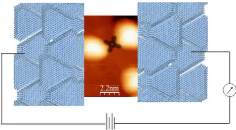
Figure 1.8: This figure suggests how a molecule could be electrically addressed using Pd clusters grown on an alumina/NiAl(110) substrate.
This figure is built on an STM image of Pd islands grown on a thin alumina layer on NiAl(110), a system that will be studied in chapter 4.
1.2 Contributions of this work
This work reported in this thesis participated in the development of the nanostencil project along two directions:
• Improvement of the AFM
It is very important to visualize all the steps of the fabrication of the device by imaging. The only technique able to image single molecule on insulating substrate is AFM in the so-called Frequency Modulation (FM-AFM) or Non-Contact mode (NC-AFM). This technique is briefly presented in the next part of this chapter.
• Investigation of Pd/alumina/NiAl(110)
As already mentioned, the nanostencil technique requires finding a suitable metal/insulator system. The ideal system would exhibit a two-dimensional, epitaxial growth of a crystalline metallic deposit. Unfortunately, the growth mode for most metal/insulator system is 3D, mainly because the surface free energy of insulators is usually much lower than that of metals. Nevertheless, one can hope to achieve 2D growth even in these conditions if kinetic limitations come into play. We have chosen to investigate the alumina/NiAl(110), which is made by oxidation of NiAl(110), because it was reported that Pd grows on this surface in the form of flat crystalline islands [Yoshitake2006, Hanssen1999], which, as already suggested (figure 1.8) could be used as intermediate scale electrodes to electrically address a molecule. The results which have been obtained from STM and STS measurement on this insulating layer as well as preliminary studies of Pd deposition on it are reported in chapter 4: "The Pd/Al10O13/NiAl(110) system".
1.2.1 Non–Contact Atomic Force Microscopy
1.2.1.1 NC-AFM history
Since its invention in 1986 [Bining1986], Atomic Force Microscopy has developed beyond all expectations. It is nowadays used in many scientific and technological domains to
Chapter 1 General Introduction
ultra high vacuum (UHV) to liquids. This success relies heavily on the availability of
microfabricated force sensors, which convert the force felt by a sharp tip positioned in the
vicinity of the sample into a displacement, which can be measured by different techniques. These sensors have generally a diving board, cantilever beam geometry. Today, a large number of different cantilever types, differing by their resonant frequency f0, stiffness k, and
quality factor Q are commercially available (figure 1.9).
AFM was originally used in the static mode, where the quasi-static deflection of a low k cantilever (typically 0.1 N/m) is used to get a topography of the surface. While this mode can produce nice images displaying the atomic periodicity of crystalline surfaces, it is not capable of true atomic resolution except under very special circumstances [Giessibl1992]. The low k necessary to improve the force sensitivity makes the static mode prone to jump-to-contact instabilities and the tip-substrate interaction is generally quite strong, due to long-range van der Waals forces that press the tip against the substrate.
a) b)
Figure 1.9: A typical NC-AFM cantilever chip, from Nano science Instruments, a) The entire chip top view and cross section views, in b) a zoom on the cantilever, top view and side view.
In dynamic modes, which were developed to limit this tip-surface interaction, the cantilever is vibrated near its resonance frequency. There are two basic methods for dynamic operation: amplitude-modulation (AM-AFM) and frequency-modulation (FM-AFM) or NC-AFM. In AM-AFM [Martin1987], the cantilever is driven at a fixed, near-resonance frequency. The changes in the amplitude and the phase of the oscillator while the tip scans over the sample surface are then used as imaging signals. Designed originally to use long-range forces (electrical or magnetic forces) for intermediate scale imaging (10 nm resolution), this mode was later used at closer distance, to reach the repulsive tip-sample interaction regime. This "Tapping Mode" [Zhong1993] is now used routinely for most ambient conditions AFM investigations. It allows to get true atomic resolution [Erlandsson1997], but is limited by its
inherent slowness: the time scale for amplitude changes in AM-AFM, given by τ~2Q/ω0, is proportional to Q. But the performance of cantilevers, limited by their thermal noise, is inversely proportional to Q. Increasing Q in AM-AFM improves the signal-to-noise ratio, but
in the same time, leads to prohibitively long acquisition times.
The solution to this problem was proposed by Albrecht and co-workers [Albrecht1991] in the founding paper of FM-AFM. In this method, the cantilever is embedded in a positive feedback loop that oscillates at the cantilever resonance frequency while another loop maintains its oscillation amplitude at a pre-set value. In contrast to the AM method, where the frequency is externally fixed, the resonance frequency of the cantilever in the FM method varies under the influence of the tip-sample forces. The time scale for these variations is only limited by the time scale of the oscillation itself (~1/f0). The FM technique is thus potentially
much faster than the AM method.
True atomic resolution was first obtained in NC-AFM by Giessibl [Giessibl1995], and Kitamura and Iwatsuki [Kitamura1995] in 1995. It has now been achieved on a wide variety of surfaces (metals, covalent or ionic semiconductors, covalent or ionic insulators) and the technique, after been used in UHV for a long time, is now adapted to ambient conditions and to liquids, especially for applications in biology [Fukuma2007].
1.2.1.2 NC-AFM principle
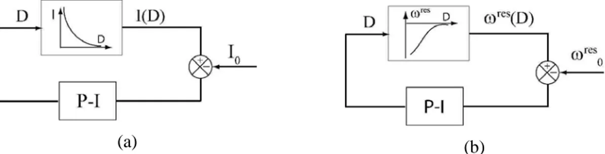
NC-AFM is compared to STM in figure 1.10. In STM, one uses the tunneling current I to keep the tip-surface distance at a constant value while scanning the surface with the tip. This is achieved by a feedback loop in which the tunneling current is compared with a preset value I0, and the resulting error signal I - I0 is used to act on the tip position D via a
Proportional-Integral (P-I) corrector and a piezoceramic actuator (figure 1.10a). The excellent resolution of STM stems from the exponential dependence of the tunneling current on the distance.
(a) (b)
Chapter 1 General Introduction
At this level of description, NC-AFM works in a similar way. Instead of using the I(D) characteristics of the tunneling junction, one relies on the ωres(D) curve of an oscillator that uses the cantilever as its frequency determining element. The resonant frequency of the oscillator ωres depends on the force exerted by the substrate on the tip that in turn depends on the tip-substrate distance, as illustrated by the curve in figure 1.10b. ωres(D) is compared to a preset value ωres0 and the resulting error signal ωres - ωres0 is used to act on the tip position D.
The complexity of NC-AFM comes from the way this oscillator is implemented. In the following, we built it step by step.
The cantilever can be considered as a one degree of freedom harmonic oscillator, described by a harmonic transfer function Cl(ω) (figure 1.11) that writes:
) ( 1 ) ( ) ( ) ( 0 2 0 2 2 0 ωω ω ω ω ω ω ω Q j k F z Cl + − = = (1.1)
where ω0is the resonance frequency of the cantilever, k its stiffness and Q its quality factor.
Figure 1.11: Block representing the harmonic transfer function of the cantilever
The block diagram of figure 1.12 shows how the NC-AFM oscillator is built. The cantilever is inserted in a positive feedback loop including a block of harmonic transfer function G(ω).
Figure 1.12: Block diagram of the NC-AFM oscillator
The global transfer function reads then:
) ( ) ( 1 ) ( ) ( ) ( ) ( ω ωω ω ω ω G Cl Cl F z T − = =
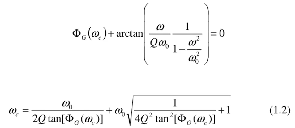
This system will oscillate at ω = ωc if: 1−Cl(ω)G(ω)=0, that is:
0 ) ( ) ( 1 ) ( ) ( = Φ + Φ = c G c Cl c c G Cl ω ω ω ω
where ΦCl and ΦG are the arguments of Cl(ω) and G(ω). Using the second condition and equation (1.1), one obtains:
( )
0 1 1 arctan 2 0 2 0 = − + Φ ω ω ω ω ω Q c G and: 1 )] ( [ tan 4 1 )] ( tan[ 2 0 2 2 0 + Φ + Φ = c G c G c Q Q ω ω ω ω ω (1.2)This relation shows that, in general, ωc, the resonant frequency of the oscillator differs from ω0, the resonant frequency of the cantilever. The phase of the controller G fixes ωc. This
oscillator is a phase-controlled oscillator [Dürig1997]. In addition, for an arbitrary phase setting ΦG, ωc depends on the quality factor Q. This means that if the tip-substrate force is
non-conservative, but becomes dissipative, "topographic" information, which is supposed to be carried by the conservative force will be mixed with "dissipation" information carried by the non-conservative component of the tip-substrate force. Relation (1.2) shows that the only setting which can decouple the "topographic" and "dissipation" channels is ΦG =π/2. In this case, ωc = ω0, the resonant frequency of the oscillator coincides with the resonant frequency
of the cantilever.
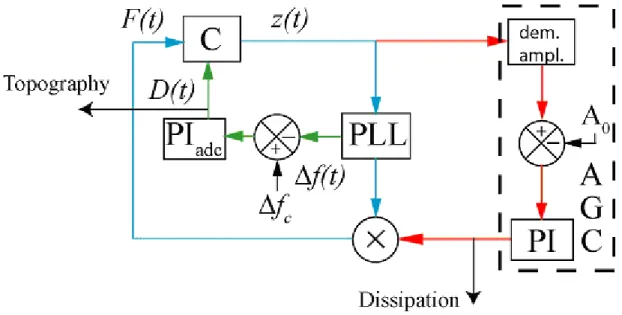
But with this phase setting, the system described by the diagram of figure 1.12 is not stable; it is then necessary to control the oscillation amplitude, as shown in figure 1.13.
Figure 1.13: Implementation of the amplitude controlled positive feedback NC-AFM oscillator
Chapter 1 General Introduction
second to synthesize a sinusoidal carrier at the oscillation frequency and with a phase satisfying the ΦG =π /2 condition mentioned previously. The second loop, in red, includes an amplitude demodulator. The oscillation amplitude A is measured and compared to a preset value A0. The error signal A - A0 is filtered by a P-I corrector and then multiplied with the
carrier produced by the PLL to produce the excitation force necessary to maintain the oscillation amplitude at A0. From this excitation force, it is straightforward to extract the
energy which is dissipated to maintain the oscillation amplitude at A0. It includes two parts,
the first one that corresponds to the energy dissipated in the cantilever, due to the finite value of the Q factor and the second one that corresponds to the non-conservative component of the tip-substrate interaction force.
Combining this oscillator with the distance regulation loop presented in figure 1.10b gives finally the diagram for the complete control system shown in figure 1.14. It is seen that two images are simultaneously produced: A "topographic image" built from the piezo position D necessary to maintain the frequency shift at ∆fc and a "dissipation" image built from the
excitation force necessary to maintain the amplitude at A0.
Figure 1.14: Complete diagram of the NC-AFM
1.2.1.3 Optical beam deflection sensor
Several methods have been proposed and developed to detect the cantilever deflection: the original electron tunneling method [Binnig1986], optical interferometry [Rugar1989], piezoelectrical detection [Giessibl2002], piezoresistive detection [Tortonese1993] or optical
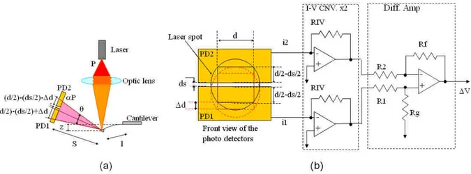
beam deflection [Meyer1988]. Our setup is based on the Optical Beam Deflection (OBD) method, illustrated in fig. 1.15.
Figure 1.15:.The optical beam deflection method.
A light source (laser or light-emitting diode) is focused by an optical system of lenses onto the back of a cantilever. The reflected light goes to a photo-detector sensor that is split into four quadrants. The small displacements of the extremity of the cantilever are magnified by an optical lever effect. By combining the electrical signals from the four quadrants of the photodiode, it is possible to measure the vertical deflection of the cantilever, but also its lateral torsion, which is related to the friction of the tip on the substrate.
At the beginning of this thesis, the RT Omicron AFM head was equipped with a light emitting diode (LED). Previous experiments had convinced us that the performance of this head was severely limited by this light source, mainly because of its large size, leading to the impossibility to properly focus it on the cantilever. It was then decided to replace the LED by a superluminescent laser diode. The way this modification was performed and the characterization of the resulting improvement in the performance of the AFM head are reported in detail in chapter 2: "Optimization of the AFM beam deflection sensor".
Following this instrumentation work, experiments were carried on a reference surface for NC-AFM: KBr(001). The initial goal was to test the new setup, but the work went much farther. The main result is the demonstration that the atomic contrast observed in the dissipation images of KBr(001) is related to an adhesion hysteresis phenomenon, which involves a two-level system localized near the apex of the tip. This demonstration is based on the observation of a reversible change in the polarity of a particular tip when crossing monoatomic steps
Chapter 1 General Introduction
∆f(z) curves with the same tip. These studies are described in chapter 3: "NC-AFM study on
KBr(001)".
These experiments were followed by different attempts to adsorb and image molecules on the same surface. Preliminary observations, which are far from being understood, but which could suggest other, more precise and controlled experiments are briefly discussed in the last chapter: "Conclusions and perspectives".
CHAPTER 2
Optimization of the AFM beam deflection sensor
2.1 Introduction
In this chapter, we describe the modifications that were made on the RT STM/AFM head from Omicron [Omicron1997] during this thesis. The experiments performed with the optimized setup are described in chapter 3: "NC-AFM study of KBr(001) ".
In 2.1, we derive an analytical expression giving the sensitivity (in Vm-1) of the beam deflection sensor in terms of the different parameters of the device. This expression is useful to discuss how the sensor can be optimized. But it is not enough to optimize the sensitivity. Noise should also be considered, as what we are interested in is to improve the signal to noise ratio. The different sources that contribute to the noise of the instrument are discussed in 2.2. The modifications of the RT STM/AFM head are described in 2.3. Measurements of the noise spectrum of the cantilever displacement were performed in order to characterize quantitatively the new optical beam deflection system. They are presented and analyzed in 2.4. We show that, once the stiffness of the lever is known (part 2.5), this analysis provides a non-destructive method to measure the sensitivity of the instrument that is useful to calibrate the oscillation amplitude of the cantilever, which is an essential experimental parameter for NC-AFM.
Chapter 2: Optimization of the AFM beam deflection sensor
2.2. Sensitivity of the optical beam method
Fig. 2.1: a) Optical beam deflection set-up, b) front view of the photo-detectors and scheme of the pre-amplification electronics.
The basic set-up of the Optical Beam Deflection (OBD) method is illustrated in fig. 2.1, [Sarid1991, Fukuma2005]. A light source (laser or light-emitting diode) is focused by an optical system of lenses onto the back of a cantilever. The reflected light goes to a photo-detector sensor that is split in two parts, PD1 and PD2. l is the length of the lever, S the distance from the end of the lever to the photo detectors, d × d the surface of the optical spot on the photo-detector, P the optical power at the entrance of the system, and α the power attenuation coefficient due to imperfections in the optical path (figure 2.1a). The efficiency of the photo-detector is given by its responsivity η (in A/W), which is the conversion coefficient between the incident optical power (in W) and the generated electrical output current (in A). The photo-induced currents i1 and i2 produced by PD1 and PD2 are converted into voltages V1 and V2 by two transimpedance amplifiers whose gain G is given by the resistor RIV, G=−RIV.
Finally a voltage ∆V =V1−V2 is produced by a difference amplifier (figure 2.1b).
The deflection of the lever under the influence of a downward force F is given by [Sarid1991]:
(
y l)
EI Fy y z 3 6 ) ( 2 − =Where y is the coordinate along the length of the cantilever, E the Young’s modulus, and I the area moment of inertia. The angle at the extremity of the lever is then given by:
EI Fl dy dz l y 2 2 − = = = θ
The spring constant of the cantilever, defined as k =−F/z depends on the Young’s modulus according to EI =l3k/3. With these expressions, the angular deflection of the optical beam
θ
2 can be related to the cantilever linear deflection z by 2θ =3z/l. The linear displacement of the reflected optical beam in the photo-detector plane reads then ∆d =(3S/l)z=βz, where the amplification factor β =3S/l can easily reach 1000, with the typical values
l=0.1 mm and S= 20 mm.
When z=0, the optical spot is centered on the photo-detector. Then P1+P2=αP with
P1=P2=αP/2. In general, when the cantilever is deflected:
(
)
− + = − ∆ + = ) ( 6 1 2 2 1 2 1 ds d l Sz P ds d d P P α α and(
)
− − = − ∆ − = ) ( 6 1 2 2 1 2 2 ds d l Sz P ds d d P P α αThen the power imbalance ∆P=P1−P2 reads ∆P=6αPSz/ld, considering that ds << d (ds
is typically of the order of 20 µm, while d is usually in the millimeter range). Finally, the cantilever deflection z is detected at the output of the preamplifier by:
z ld Sz P R V V V = − =− IVηα =σ ∆ 1 2 6 (2.1)
This expression of the sensitivity σ (in Vm-1) suggests that in order to increase the displacement sensitivity of the technique, d should be as small as possible. But usually, this quantity cannot be chosen at will, as shown by Sarid [Sarid 1991]. The light beam should be focused on the cantilever, whose width is in the range of 20 µm. The spot on the photodiode is then affected by diffraction effects. For the purpose of estimation, one can use the Airy's formula, which gives the diameter q of the spot produced at a distance R from a screen with a circular aperture of diameter a illuminated by light of wavelength λ: q=1.22Rλ/a. For a light beam spot on the cantilever of diameter a, the far field diffraction limited spot size on the photo-detector is given approximately by: d =Sλ/a. Then:
z l a P R V IV λ ηα 6 − = ∆
Note that this new expression is independent of the distance S from the lever to the photo-detector.
All the parameters that influence the displacement sensitivity of the method appear in this expression. To increase the sensitivity, one can:
• Increase the light source power P. Current sources have powers in the mW range. A limitation is the heating of the cantilever by the absorbed light.
Chapter 2: Optimization of the AFM beam deflection sensor
• Increase α, the light transmission coefficient of the system. This includes minimizing reflections at the different interfaces, optical absorption by the different components and using reflective (metallized) cantilevers.
• Use an efficient photodiode, with a as high as possible value for the responsivity η. There is not much to gain here, as most of the Si PIN photodiodes used for AFM have comparable responsivities, which, depending on the wavelength, vary between 0.4 and 0.7 A/W.
• Maximize a, the size of the light spot on the cantilever to minimize the diffraction which tends to enlarge the size of the spot on the photo-detector. Of course a should stay below w, the width of the cantilever.
• Minimize l, the length of the cantilever. The length of typical commercial cantilevers varies between 100 µm and 200 µm. This choice is related to the desired resonance frequency of the cantilever.
• Minimize λ, the wavelength of the light used. Usual diodes used in AFM cover a range of wavelengths between about 600 nm and 1000 nm.
• Increase the gain RIV of the preamplifier.
Sensitivity is of course an important parameter for the instrument, but it cannot be used without considering in the same time the noise that will inevitably perturb the measurements. Optimizing the sensitivity can lead to an increase of the noise. In the following, we consider the main sources of noise that affect the measurements in NC-AFM.
2.3. Sources of noise
Two types of noise can be distinguished in NC-AFM, the thermal noise of the cantilever, and the noise of the deflection sensor. The thermal noise of the cantilever is a fundamental noise arising from the thermal fluctuations of the cantilever. It is intrinsic, and does not depend on the type of deflection sensor used. The most important noises present in the OBD method according to [Fukuma2005] are the Johnson noise of the conversion resistors of the preamplifier, the shot noise of the photo-detectors and the noise of the optical source. In the following, we discuss first the noise of the OBD sensor, then the thermal noise of the cantilever. To get the expressions that will be used to interpret the experiments discussed in the following of this chapter, we need first to introduce the Omicron preamplifier, which in
contrast to the basic preamplifier shown in figure 2.1 uses a four-quadrants photodiode (figure 2.2).
Figure 2.2: The Omicron Pre-Amplifier electronic circuit with the four-quadrants photo-detector used in the AFM/STM RT-UHV head.
Each of these four quadrants has its own I-V converter. Three different signals can be extracted from different combinations of their outputs A, B, C and D:
• The friction signal, related to the lateral displacement of the optical spot on the photodiode, given by 5× [(A+B) – (C+D)].
• The average (A+B+C+D)/4, which reads:
4 /
IV
total PR
V =ηα (2.2)
• The topography signal, 5×[(B+D)-(A+C)] expressed from (2.1) as:
z ld S PR VFN IV 6 5ηα = (2.3) or: z V z V ld S VFN = total = µ total 120 (2.4) where µVtotalis the displacement sensitivity.
2.3.1 The shot noise
The shot noise affecting an electrical current is related to the discreteness of the electron charge. It appears each time the discrete nature of electrons has to be taken into account in the description of the phenomenon. For instance, it affects the tunneling current across a barrier, but not the current in a good conductor. In the case of photo-detection, the electrons
Chapter 2: Optimization of the AFM beam deflection sensor
contributing to the photocurrent are generated by discrete events, described as the absorption of a photon of the incident light.
The current shot noise Power Spectral Density (PSD) of the photocurrent I is expressed asSIshot
( )
f =2eI, where e is the magnitude of the electron charge [Schottky1918]. Eachquadrant of the photo-detector generates its own noise. The corresponding voltage noise after the transimpedance amplifiers of the circuit presented in figure 2.2 is given by:
( )
f e I I I I R R e PSVshot =2 ( A+ B + C + D) IV2 =2 IV2 ηα
The corresponding noise voltage at the output of the preamplifier is then given by:
( )
IV IV IV total shot V f R e P R e P R eV S FN 2 2 2 2 200 50 2 5 × = = = ηα ηα (2.5)2.3.2 The Johnson noise
Johnson noise [Johnson1928, Nyquist1928] is the electronic noise generated by the thermal agitation of the charged carriers inside an electrical conductor at equilibrium. It is a consequence of the fluctuation-dissipation theorem [Callen1951]. To each of the converting resistors RIV is associated a voltage PSD:
IV B johnson
V f k TR
S ( )=4 (2.6) where kBT is thermal energy. The corresponding noise voltage at the output of the
preamplifier is then given by:
(
)
B IV johnson VB johnson VB johnson VB johnson VA Johnson V f S S S S k TR S FN ( ) 5 400 2 = × + + + = (2.7)2.3.3 The optical source noise
Light emitting diodes (LED) and lasers are the two most common light sources used in AFM. Lasers are affected by specific noise, which we briefly describe in the following. LED have also their specific noise and suffer from a major drawback: the size of their equivalent source is usually quite large, making them difficult to focus. This is the main reason for the head modification that is described in part 2.4.
2.3.3.1. Laser noises
It is well known that the beam intensity, the beam direction, and the profile of the beam of a laser fluctuate. The main source of these fluctuations is mode hopping which corresponds to transitions between different modes of the laser resonator. These hops are generally provoked by external disturbances, such as a variation of the temperature or, in the case of optical
feedback, when some light is reflected back into the laser cavity. It has been shown
[Ojima1986] that this noise can be largely reduced by modulating the laser diode current at high frequency, which causes the diode to "average" over its accessible modes. This trick is commonly used in videodisc players [Ojima1986] and has been adapted to laser diodes used for AFM [Kassies2004, Fukuma2005]. It has the other advantage of eliminating the interferences between the light reflected by the cantilever and the light scattered by the sample, which are commonly observed in AFM, because it reduces drastically the coherence length of the laser. Another type of source, which presents the same advantages, is the superluminescent diode (SLD), which will be introduced in 2.4.1.
Let us note that independently of these considerations, the noise generated by the intensity fluctuations is generally negligible in AFM because what is measured is the difference
(B+D)-(A+C): most of the laser intensity fluctuations are eliminated as a common mode noise
by the preamplifier. Furthermore, the noise induced by beam direction and profile fluctuations can be diminished by using a single mode optical fiber to couple the laser diode to the focusing optics of the OBD sensor.
2.3.4 The cantilever thermal noise
The energy of a system in contact with a thermostat at finite temperature T fluctuates, by an amount which is very small for a macroscopic object, but that becomes significant for a microscopic and relatively soft object such as an AFM cantilever. To a very good approximation, a cantilever can be considered as a one degree of freedom harmonic oscillator. As stated by the equipartition theorem, the average energy for each quadratic term in its Hamiltonian should be given by 1/2kBT, where k is the Boltzmann constant. The mean B
value of the potential energy is then given by:
T k kz B 2 1 2 1 2 =
from which the variance of the displacement z, which characterizes the fluctuations of the cantilever can be extracted:
k T k
z2 = B
(2.8) This variance can be related to SThermalz ( f), the power spectral density of the displacement z, by:
∫
∞=
Chapter 2: Optimization of the AFM beam deflection sensor
It is usual to express these displacement fluctuations in terms of the input of the force-displacement harmonic transfer function of the cantilever:
) ( ) ( ) (f C f 2 S f S ForceThermal Thermal z = (2.10)
Where C(f) is the free cantilever harmonic transfer function and SForceThermal( f) is the power spectral density of the force that has to be applied to the ideal, noiseless cantilever to produce the displacement fluctuations characterized by SThermalz ( f). C(f) is readily derived from Newton's equation: m&z&=−kz−γ z&+F(t). Were γ is a viscosity, by injecting
) 2 exp( ) (f j ft z z= π and F(t)=F(f)exp(j2πft): Q ff j f f k f f C o o o + − = 2 2 2 ) ( (2.11)
where f0 =1/2π k/m is the resonance frequency of the cantilever and Q=2πmf0/γ is its quality factor. Combining (2.8-11), we get:
∫
∞ − + = = 0 2 2 2 2 2 ) (f df S Q ff j f f k f k T k z ForceThermal o o o BIt turns out that SForceThermal( f) is independent of frequency. The integral can then be evaluated giving finally: T k Q f T kk S B o B thermal Force γ π 4 2 = = (2.12)
The thermal force fluctuations depend only on the dissipation. This is another expression of the fluctuation-dissipation theorem and the expression (2.12) is analogous to the expression (2.6) we already used for the voltage noise in a resistor, where R has been replaced by γ. Finally, the contribution of the cantilever thermal noise at the output of the preamplifier reads, from (2.4, 2.10, 2.11, 2.12):
[
2 2 2 2 2]
2 3 2 2 2 2 ) ( ) ( 2 ) ( total o o o B total thermal Force Thermal V V f f f f Q k Q f T k V S f C S FN =µ =µ π − + (2.13)2.4. Modifications of the RT AFM Omicron head
The RT Omicron AFM head was used before this thesis, in particular during the PhD work of Jérôme Polesel Maris [Polesel2005] to investigate different surfaces (Al2O3(0001), TiO2(110),
KBr(100),...). During these experiments, a number of problems were identified, which lead to the conclusion that this set-up was far from state-of-the-art, rendering impossible certain experiments. In particular:
• It was impossible to work below a frequency shift |∆f|≈10 Hz • It was impossible to work with an amplitude below A0≈5 nm. • It was difficult to get atomic resolution on KBr(001).
• It was impossible to see the thermal noise peak on the frequency spectrum of the cantilever displacement.
All these observations point to a bad signal-to-noise ratio. Discussions with E. Meyer and L. Nony (working at this period as a post-doctoral fellow) from the Institute of Physics in Basel convinced us that these problems originate from the deflection sensor and in particular from the LED used in this system. The main reason seemed to be that this diode is difficult to focus. The size of its spot is much larger than the typical width of a cantilever and most of the light power is lost at this level. It was then decided to replace the LED by a laser. We gratefully acknowledge the help and advices from E. Meyer and L. Nony during this modification, which is described in the following. Some of the work reported here was done by Théophile Noël (student at ISEN-Lille) during his stay in CEMES from June to September 2006.
2.4.1 The superluminescent laser diode