UNIVERSITÉ MOHAMMED V – AGDAL FACULTÉ DES SCIENCES
Rabat
N° d’ordre : 2684 Département de physique.
Laboratoire :
Laboratoire de Magnétisme et Physique des Hautes Energies.
THESE DE DOCTORAT
Présentée par Saif UR REHMAN Discipline : Physique Spécialité : Optique photonique
Experimental investigation of metal thin films using
surface plasmon resonance spectroscopy
Soutenue le 23-11-2013 devant la commission d’examen :
Président
Abdelilah BENYOUSSEF : Professeur, Faculté des Sciences, Rabat, Maroc Examinateurs:
Zouheir SEKKAT : Professeur, Faculté des Sciences, Rabat, Maroc
Abdallah EL KENZ : Professeur, Faculté des Sciences, Rabat, Maroc
Mohamed KEROUAD : Professeur, Faculté des Sciences, Meknes, Maroc
Shinji HAYASHI : Ex-Professeur, Faculté des Sciences, Kobe, Japon, Chercheur
ii
IN THE NAME OF ALLAH, THE MOST GRACIOUS,
THE MOST BENEFICENT, THE MOST MERCIFUL
iii
Dedicated to my loving Parents,
especially my Mother whose
Superfluous love and Constant
Encouragement enabled me to score
iv
ACKNOWLEDGEMENTS
Up and above anything else, all gratitude and praises are due to the Almighty Allah, the most gracious, merciful and compassionate, who gave me health, thoughts, cooperative fellows and capacitate me to achieve this goal. After Almighty Allah, praises are to his Prophet Muhammad (Peace Be Upon Him), the most perfect and exalted who is forever a source of guidance and knowledge for humanity as a whole.
I would like to express my deepest gratitude to my thesis director Professor Abdelilah BENYOUSSEF and Professor Zouheir SEKKAT (co-director) for his dedicated teaching, constant guidance, and generous support during the entire course of this research work. His stewardship of talents and his embracing cradle for the creativity will always be remembered as the role model for my teaching philosophy. I am deeply indebted to my thesis president Professor Abdelilah BENYOUSSEF and worthy committee members Professor Abdallah EL KENZ, Professor Mohamed KEROUAD and Professor Shinji HAYASHI. I thank them for their persistent support, guidance, and direction in improving my thesis. I also want to extent my gratitude towards my mentor and my dedicated outside reader, Professor Malik Maaza, for sharing his unforgettable wisdom. I will always remember this institute since; I have received so much support from MAScIR, administration assistants, and friends. Of course, I won’t forget my colleagues, Dr. Dmitry, Dr. Nouneh, Dr. Ousama, Anouar Rahmouni, Zakaria, Tarik, Ilyas and Siham. It is really fun working with all of them and I wish all the best to them. I also extend my thanks and best wishes for my country mates (Dr. M. Azeem, Dr. Junaid & Waseem etc.) for their cooperation and encouragement.
I would like to thank my parents, my sisters & brother and whole family members for being extra supportive on my education since I was a kid. My father has always been a great source of inspiration for me. I want to say to my son, Muhammad Rayyan Saif, that I will always love you and thank you for providing me the joy and the meaning of this world. Last but not least, I am forever indebted to my wife, Dr. Huma Saif, for her undivided love and her constant encouragement during the years of my doctorate studies.
TABLE OF CONTENTS
ACKNOWLEDGEMENTS iv
LIST OF TABLES v
LIST OF FIGURES vi
Chapter 1 1
1. INTRODUCTION TO SURFACE PLASMON RESONANCE 1
1.1. Introduction 1
1.2. History of surface plasmon resonance 1
1.3. Surface plasmon polariton 2
1.4. Excitation of surface plasmons 4
1.5. Localized surface plasmon resonance 6
1.6. Concept of surface plasmon resonance sensing 7
1.7. The evanescent wave 7
1.7.1. Evanescent wave sensors and surface plasmon based technique 9
1.8. Working principle of an SPR system 10
1.9. Use of gold as the metal layer 12
1.10. Theoretical Background 12
1.12. Applications of surface plasmon resonance sensing 15
1.13. References 17
Chapter 2 25
2. DETERMINATION OF THE OPTICAL THICKNESS OF SUB 10 nm METAL THIN
FILMS BY SURFACE PLASMON RESONANCE (SPR) EXPERIMENTS 25
2.1 Introduction 25
2.2. Theoretical background 28
2.3. Experimental details 29
2.4. Thin films deposition technique 31
2.4.1. Physical Vapor Deposition (PVD) 31
2.4.2. Introduction to PVD 32
2.4.3. Thermal evaporation 32
2.4.4. Heat sources 33
2.4.5. Other features 34
2.4.6. Optimization 36
2.5. Thin films preparation of gold and silver 36
2.5.1. Single layer 36
2.5.2. Double layers 36
2.6.1. Atomic force microscopy (AFM) 38 2.6.2. Introduction 38 2.6.3. History 39 2.6.4. Principle of operation 39 2.6.5. Operating modes 40 2.6.6. Non-topographic modes 41 2.7. AFM images 42
2.8. Results and discussion 45
2.8.1. Single layer films 45
2.8.2. Double layer films 47
2.9. Conclusion 54
2.10. References 55
Chapter 3 58
3. MEASUREMENTS OF THICKNESS AND OPTICAL CONSTANTS OF ULTRA THIN METAL CLUSTERS BY SURFACE PLASMON RESONANCE EXPERIMENT EXCITED
AT VARIOUS WAVELENGTHS 58
3.1. Introduction 58
3.2. Theoretical background 62
3.3. Experimental details 63
3.4.1. Thermal evaporation 65
3.5. Thin films preparation of silver and gold 65
3.5.1. Single layer 65
3.5.2. Double layers 65
3.6. Thin films characterization (morphology) 66
3.6.1. Atomic force microscopy (AFM) 66
3.6.2. Introduction 66
3.7. AFM images 67
3.8. Results and discussion 69
3.8.1. Single layer films 69
3.8.2. Double layer films 72
3.9. Conclusion 77
3.10. References 78
Chapter 4 81
4. UV PLASMONICS AND SPR INVESTIGATION OF METAL THIN FILMS AT VARIOUS
WAVELENGTHS AND REFRACTIVE INDICES (R.I) OF PRISMS 81
4.1. Introduction (UV plasmonics) 81
4.2. Importance of Al plasmonic nanostructures 83
4.4. Thin films preparation of aluminum 84
4.5. Thin films characterization (morphology) 84
4.6. Simulation 85
4.7. Al SPR results 87
4.8. SPR investigation of metal thin films at different wavelengths and refractive indices 90
4.9. Conclusion 93
4.10. References 94
Chapter 5 95
5. APPLICATION OF SPR, “ESTIMATION OF THE THICKNESS AND OPTICAL CONSTANTS OF A BIO-MATERIAL THIN LAYER (ONION EPIDERMIS)”, USING
SURFACE PLASMON RESONANCE (SPR) EXPERIMENTS 95
5.1. Introduction and motivation 95
5.2. What is Onion? 95
5.2.1. Onion epidermal cell 96
5.2.2. How to prepare an onion cell slide 97
5.2.3. Methodology 97
5.3. Biosensor applications 102
5.4. Experimental details 104
5.5. Thin films deposition technique 105
5.6. Thin films preparation of silver and gold 106
5.7. Thin films characterization (morphology) 108
5.7.1. Atomic force microscopy (AFM) 108
5.7.2. Brief introduction 108
5.8. AFM images 108
5.9. Results and discussions 110
5.10. Conclusion 114
5.11. References 115
v
LIST OF TABLES
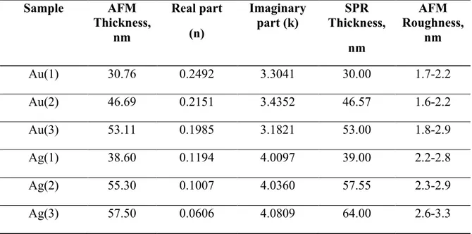
Table 2.1 The characterization of Au and Ag single layer thin films 46
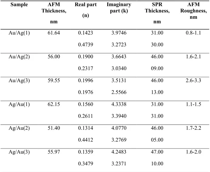
Table 2.2 Parameters of SPR of Au and Ag single layer structures 47
Table 2.3 The characterization of Au/Ag and Ag/Au double layer thin films 48 Table 2.4 Parameters of SPR by Au/Ag and Ag/Au double layer structures 50 Table 3.1 The characterization of Ag single layer thin films at various exciting wavelengths
71
Table 3.2 Parameters of SPR for Ag single layer structures 72
Table 3.3 The characterization of Ag/Au double layer thin films to measure parameters of
Au cluster at various exciting wavelengths 74
Table 3.4 Parameters of SPR for Ag/Au double layer structures 76
Table 4.1 Optical constants of metal thin layers with UV laser (405nm) 89 Table 5.1 The characterization of Au, Ag single layer and Au/Onion, Ag/Onion double layer
vi
LIST OF FIGURES
Figure 1.1 Surface plasmon waves at a metal/dielectric interface. The arrows show the
electric field lines at the interface. The magnetic field is along y direction 3
Figure 1.2 The dispersion of surface plasmons at the metal-air interface 4
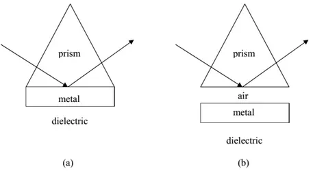
Figure 1.3 (a) Kretschmann and (b) Otto configuration of an attenuated total reflection setup for coupling surface plasmons 5
Figure 1.4 The localized surface plasmon 6
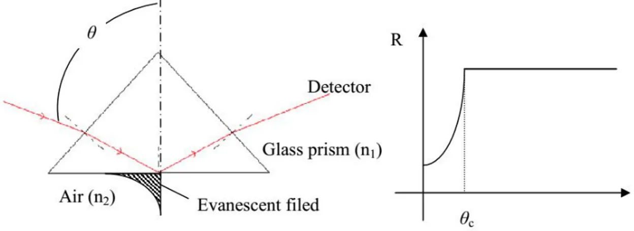
Figure 1.5 Total internal reflection 8
Figure 1.6 Total internal reflection of a plane wave at the base of a prism (left), and the reflectivity as a function of the angle of incidence (right). The reflectivity increases to unity at the critical angle for total internal reflection 9
Figure 1.7 Excitation of surface plasmon using the Kretschmann geometry 11
Figure 1.8 (a) SPR response curve by WinSpall fitting of 45nm gold thin film with 5nm chromium as bottom layer on glass substrate 14
(b) SPR response curve by WinSpall fitting of 30nm gold thin film on glass 15 (c) SPR response curve by WinSpall fitting of 45nm silver thin film on glass. 15 Figure 2.1 The excitation of surface plasmons in Kretschmann geometry 26
Figure 2.2 3D schematic plan of the constructed setup 30
Figure 2.3 A snapshot of constructed experimental setup 31
vii
Figure 2.5 Schematic of different types of evaporation sources 34
Figure 2.6 (a) NEXTDEP 400 vacuum evaporator (b) Interior outlook of evaporator chamber 35
Figure 2.7 a) Ag single layer thin films of different thicknesses (b) Au single layer thin films of different thicknesses (c) Ag/Au and Au/Ag double layer thin films of different thicknesses (d) Overall view of all single and double layer metal thin films 38
Figure 2.8 Block diagram of atomic force microscope using beam deflection detection 40
Figure 2.9 (a) Dimension Icon AFM system (b) Overall instrument view 42
Figure 2.10 Thickness measured by Atomic Force Microscope of (a) single layer of Au 30, 45 & 50 nm (b) single layer of Ag 30, 45 & 50 nm and (c) double layers of Ag/Au & Au/Ag 30/30, 45/5 & 45/5 nm thin films 44
Figure 2.11 Measured SPR data (dots) and their fitted curves (solid line) for the (a) Au and (b) Ag samples 45
Figure 2.12 Measured SPR data (dots) and corresponding fitted curves (solid line) of Au/Ag (31/30 nm) and Ag/Au (31/31 nm) double layer samples 49
Figure 2.13 SPR comparaisons of Au, Ag different thicknesses of single and bilayer metal thin films (a) Ag 45 nm with 5 & 10 nm Au on top (b) Au 45 nm with 5 & 10 nm Ag on top (c) Ag 30 nm with 30 nm Au on top and vice versa (d) comparaison of Au single and bilayer thin films (e) comparaison of Au single and bilayer thin films 53
Figure 3.1 The excitation of surface plasmons in Kretschmann geometry 59
Figure 3.2 3D schematic plan of the constructed setup 64
viii
Figure 3.4 (a) Ag single layer thin films of different thicknesses (b) Ag/Au double layer thin
films of different thicknesses 66
Figure 3.5 Thickness measured by Atomic Force Microscope of (a) single layer of Ag thin film (b) Double layers of Ag/Au thin films 68
Figure 3.6 (a), (b) and (c) Measured SPR data (dots) and their fitted curves (solid line) for Ag single layer samples excited at various wavelengths (d) Comparison of Ag single layer samples at 633, 532 and 405nm 69
Figure 3.7 (a), (b) and (c) Measured SPR data (dots) and corresponding fitted curves (solid line) of Ag/Au(1) and Ag/Au(2) double layer samples at various wavelengths (d) Comparison of Ag/Au double layer samples at 633, 532 and 405nm 75
Figure 4.1 UV plasmonics. Real and imaginary parts of dielectric functions (as functions of wavelength) of aluminum, rhodium, gold, and silver in UV and visible ranges. Aluminum behaves as a plamonic material in the deep-UV range [2] 82
Figure 4.2 A photograph of constructed experimental setup 83
Figure 4.3 Single and double layer thin films of Al and Al/Au 84
Figure 4.4 AFM images of single and double layer thin films of Al and Al/Au 85
Figure 4.5 SPR response curve by WinSpall fitting (a) Al single layer of 21 nm (b) Al/Au 16+6 nm and (c) Al/Au 17+2 nm bilayers 86
Figure 4.6 Comparison of SPR response curves of Al single and bilayers at 405 nm 87
Figure 4.7 Comparison of SPR response curves of Al single and bilayers (a) excited at 532 nm laser (b) excited at 632.8 nm laser 88 Figure 4.8 Comparison of SPR response curves of silver single and bilayers at 405 nm 89
ix
Figure 4.9 Comparison of SPR response curves of (a) silver (Ag) and (b) gold (Au) single layer thin films at 632.8nm wavelength and different prisms 91 Figure 4.10 Comparison of SPR response curves of (a) silver (Ag) and (b) gold (Au) single layer thin films at 532nm wavelength and different prisms 92 Figure 5.1 Onion types and onion epidermis with a chart of nutritional values 97 Figure 5.2 A simple microscope and dye, pin, onion membrane, slide and cover slip 98 Figure 5.3 The SPR configuration for the excitation of surface plasmons in Kretschmann
geometry 101
Figure 5.4 3D schematic plan of the constructed setup 105
Figure 5.5 (a) Ag single layer thin films of 45 nm with attached thin epidermis (b) Au single
layer thin films of 45 nm with attached thin epidermis 107
(c) Light microscope images of Onion epidermis at different magnification 107 Figure 5.6 Thickness and roughness measured by Atomic Force Microscope of (a) single
layer of Au thin film (b) single layer of Ag thin film 110
Figure 5.7 (a, b, c and d) Measured SPR data (dots) and their fitted curves (solid line) for Ag, Ag/Onion, Au and Au/Onion single and bilayer samples excited at 632.8 nm
wavelength 111
Figure 5.8 Comparisons of single and bilayer thin films at 632.8 nm 113
Résumé
L’excitation plasmonique et l'interaction lumière-matière sous-longueur d'onde associée a ouvert de nouvelles voies pour la recherche issue des observations et des modèles théoriques de plusieurs propriétés uniques des ondes plasmonique de surface se propageant dans les interfaces métal-diélectriques. Cette thèse est une description détaillée de l'étude expérimentale de la résonance plasmonique de surface (SPR) de couches minces métalliques. Le chapitre 1 décrit les principes de base du phénomène de la résonance plasmonique de surface (SPR). Le chapitre 2 présente les données expérimentales de la SPR qui se produit à l'interface entre l'air et des couches simples et bimétalliques d'argent (Ag) et d'or (Au) des films minces déposés sur des substrats de verre. Le chapitre 3 expose les mesures de l'épaisseur et des paramètres optiques des groupes ultra-minces en métal d'or en utilisant la technique SPR à différentes longueurs d'onde (633 nm, 532 nm et 405 nm). Ce résultat est dû à la configuration double couches des fines barres métalliques. Le chapitre 4 traite de la plasmonique UV d'aluminium (Al) des films minces et les courbes de réponse SPR de l'argent et des couches minces d'or (simple, bicouches) excités à différentes sources laser et de divers matériaux de prisme. Dans le chapitre 5, nous excitons SPR d'un naturel mince épiderme de bulbe d'oignon (Allium Cepa), qui est un matériau biologique dont la surface d’épaisseur 45 nm est un empilement de films d'or et d'argent pour observer le changement en mode SPR. La microscopie à force atomique (AFM) a été utilisée pour caractériser l'épaisseur et la rugosité des couches d'argent, d'or et d’aluminium simples, films bicouche, et nous avons utilisé les épaisseurs mesurées par AFM, afin de déterminer (i) les indices de réfraction des films métalliques, et (ii) les paramètres de courbes SPR, telles que la hauteur, la largeur totale à mi-hauteur de la SPR dip, inclinaison moyenne des pentes. L’amélioration du champ SPR des échantillons de film a été calculée sur la base des propriétés mesurées des films. Les résultats obtenus par des mesures expérimentales sont en accord avec l'analyse AFM. L'originalité de notre configuration SPR est l'estimation de l'épaisseur et les constantes optiques des couches minces et des groupes métalliques ultra-minces (5 nm) de couches simples et doubles. Il a été constaté que la partie réelle de l'indice de réfraction (n) de la couche d’argent diminue avec l'augmentation de l'épaisseur du film à des longueurs d'onde d’excitations de 633, 532 et 405 nm. La partie réelle de l'indice de réfraction de la couche d’or (groupe métalliques) ultra-mince augmente avec l'augmentation de l'épaisseur (de 5 à 9 nm), tandis que n de couches simples d’or diminue avec l'augmentation de l'épaisseur pour des épaisseurs supérieures à 30 nm. Il est identifié qu'il atteigne une valeur maximale à des épaisseurs entre 10 et 30 de nm. Également, il a été observé que 633 nm est une source d'excitation plus fiable pour mesurer l'épaisseur de la SPR en dessous de 10 nm de groupes métalliques d'or relativement 532 et 405 nm de longueurs d'onde. L'originalité de cette thèse réside dans les points suivants: les mesures des constantes optiques des groupes métalliques à l'échelle nanométrique; l'étude des couches bimétalliques par rapport à la pénétration de l'onde évanescente, ainsi que l'observation des différentes configurations de plusieurs couches métalliques simples et doubles à différentes longueurs d'onde plasmonique.
Mots clés: Résonance plasmonique de surface, les couches minces, les constantes optiques, des
Abstract
Plasmonic excitation and the associated sub-wavelength light-matter interaction has opened new and fascinating avenues for research that originates from the observations and theoretical predictions of several unique properties of surface plasmon waves propagating on metal-dielectric interfaces. This dissertation provides the detail description about experimental study of surface plasmon resonance (SPR) of metal thin films. Chapter 1 describes the basics of surface plasmon resonance (SPR) phenomenon. Chapter 2 discusses experimental data of SPR occurring at the interface between air and single and bimetallic layers of silver (Ag) and gold (Au) thin films deposited on glass substrates. Chapter 3 exposes the measurements of thickness and optical parameters of ultra-thin metal clusters of gold using SPR technique at various wavelengths of 633 nm, 532 nm and 405 nm. This finding is due to the double layer configuration of the metal thin bars. Chapter 4 deals with UV plasmonics of aluminum (Al) thin films and SPR response curves of silver and gold thin films (single, bilayers) excited at different laser sources and various prism materials. In Chapter 5, we excite SPR of a natural thin, epidermis of Onion bulb (Allium Cepa), a biological material which is stacked onto the surface of 45 nm thick films of gold and silver to observe a shift in SPR mode. We performed atomic force microscopy (AFM) measurements for characterizing the thickness and roughness of silver, gold and aluminum single, bilayer films; and we used the thicknesses measured by AFM, to determine (i) the refractive indices of the metal films, and (ii) parameters of SPR curves, such as height, full width at half maximum of SPR dip, average inclination of the slopes. SPR Field enhancement of the film samples was calculated based on the films measured properties. The results obtained by experimental measurements are in good agreement with AFM analysis. The attractiveness of home-made SPR setup in our case is the estimation of thickness and optical constants of thin films and ultra-thin metal clusters (5 nm) of single and double layers. We found that the real part of refractive index (n) of Ag single layer decreases with increasing film thickness at 633, 532 and 405 nm exciting wavelengths. The real part of refractive index of Au ultra-thin layer (metal clusters) increases with increasing thickness from 5 to 9 nm, while n of Au normal single layers decreases with increasing thickness for thicknesses above 30 nm. It is identified that it achieves a maximum value in 10-30 nm thickness region. It is also observed that 633 nm is a more reliable exciting source for measuring the SPR thickness of below 10 nm metal clusters of gold relatively 532 and 405 nm wavelengths. The originality of this thesis lies into the following points: the measurements of the optical constants of nanometer scale metal clusters; the study of bimetallic layers with respect to evanescent wave penetration; as well as the observation of different configurations of several metal single and double layers at different palsmon wavelengths.
Key words: Surface plasmon resonance, thin films, optical constants, ultra-thin gold clusters and
Chapter 1
INTRODUCTION TO SURFACE
PLASMON RESONANCE
1
Chapter 1
1. INTRODUCTION TO SURFACE PLASMON RESONANCE 1.1. Introduction
A surface plasmon is a quantum of a collective plasma oscillation confined at a dielectric-metal interface [1,2]. It can be excited by electromagnetic radiation by matching the momentum of the incident photons to that of the surface plasmon or so-called surface plasmon resonance (SPR) condition. The excited surface plasmon or the surface plasmon polariton can propagate along a planar metal surface or can be localized on metallic nanoparticles or nanostructures. The induced electromagnetic field on metal surface decays exponentially into both media as a surface confined evanescent wave. Since the induced field is very sensitive to the variations of the dielectric medium in proximity to a metal surface, a small change in the optical properties of the dielectric medium can be quantitatively analyzed for the sensing purposes.
Sensors based on surface plasmon resonance have gained increasing popularity. One example is surface plasmon resonance spectroscopy, which is able to measure the binding of analytes to the functionalized surfaces without any labeling and is able to measure the binding events in real time [3-6]. Its label-free advantage has been exploited for biosensing applications such as the development of immune sensors, [7-9] proteomic technology, [10,11] drug discovery, [12,13] DNA sensors, [14,15] and as a tool for studying biomolecular interactions [16,17]. Several reviews of surface plasmon resonance spectroscopy have been published [18-20]. On the other hand, the large field enhancement associated with SPR provides a basis for many surface analytical techniques such as surface enhanced Raman spectroscopy, [21-24] surface enhanced fluorescence spectroscopy, [25,26] and surface enhanced infrared absorption [27-29].
1.2. History of surface plasmon resonance
Homola et al. and Sharma et al. have provided a detailed history of surface plasmon resonance [30,31]. It is summarized in this section with reference to the original papers.
As early as 1907, Zenneck [32] and in 1909, Sommerfeld [33] demonstrated and formulated the existence and properties of radio frequency surface Electromagnetic (EM) waves at the interface of a loss-free medium and a “lossy” dielectric, or a metal. The main stride towards the existence
2
of Surface Plasmon (SP) waves was made in 1957, when Ritchie derived the energy distribution of a fast electron losing energy to the conduction electrons in a metallic foil and proposed that the energy loss is due to the surface plasmon excitation [34]. Ritchie’s theory was further supported by Powell and Swan (1960) by detecting the excitation of surface plasmons in aluminum and magnesium through the use of electrons [35]. Their work was followed by Stern and Ferrell, who in the same year derived the condition of resonance for surface plasmon modes and showed that the surface wave involved electromagnetic radiation coupled to surface plasmons [36].
In 1968, Otto introduced the method of attenuated total reflection (ATR) for resonant excitation of surface plasmon waves by light [37]. His idea involved using a prism near the metal vacuum interface, so that the surface plasmon waves are excited optically by the evanescent waves present in total reflection. However, the most popular and widely used method till now is the Kretschmann configuration proposed in 1968 [38]. The Kretschmann configuration made the practical and commercial use of surface plasmon resonance (SPR) possible. Instead of a finite air gap between the prism base and the metal substrate as in Otto configuration, a thin metal layer (10nm-100nm) is kept in contact with the prism base.
The prospects of surface plasmon resonance (SPR) sensing in the field of thin film characterization and monitoring electrochemical interfaces, were further realized with the work from Pockrand et al. and Gordon et al. [39,40]. During the early 1980’s, Nylander et al., and Lied berg et al. demonstrated the use of SPR for gas-detection and bio-sensing [41-43]. From that time onwards, the surface plasmon resonance technique has been in wide-spread use for characterization and quantization of physical, chemical and biological interactions. Since 1990, several companies have launched the surface plasmon resonance biosensors commercially [30]. 1.3. Surface plasmon polariton
Excitation of a surface plasmon by a photon is called a surface plasmon polariton or a surface plasmon wave. It is a collective oscillation of electrons or a plasma wave near the surface of a metal, also known as the non radiative evanescent wave [1]. Figure 1.1 depicts the surface plasmon waves at a metal-dielectric interface. Maxwell’s equations consist of four partial differential equations which describe the properties of the electric and magnetic fields under an
3
electromagnetic perturbation. We can use Maxwell’s equations to describe the generation of a surface plasmon polariton [1,44]. Figure 1.1 shows a system with two media, a dielectric and a metal. When light impinges at the interface between the two media, the linear momentum of the light is conserved across the two medium.
Figure 1.1 Surface plasmon waves at a metal/dielectric interface. The arrows show the electric field lines at the interface. The magnetic field is along y direction.
The derivation of Maxwell’s equation leads to a simple relationship between the relative permittivity and the normal components of the wave vectors of the applied field in both media shown in equation 1.1 [1]. d m dz mz k k Eq. 1.1
Where kdz and kmz are the z-components of the wave vectors of the radiation in a dielectric
medium and in a metal respectively.
By satisfying Maxwell’s equations with the boundary conditions, the wave vector of the surface plasmon polariton (kSPW) can be related to the wave vector of the radiation (k) and the dielectric
4 d d m spw m k k Eq. 1.2
From the equation 1.2, the generation of surface plasmon polaritons requires a negative dielectric constant for the metal and |εm|> εd. Metals with a negative dielectric constant include silver, gold,
copper and aluminium and of which silver and gold are more commonly used. Silver is used as it provides a sharp SPR resonance peak while gold is used due to its stability.
There are two types of surface plasmon polariton: propagating and localized surface plasmon polariton. The generation of a propagating surface plasmon polariton on the planar surface is discussed in section 1.4 while the generation of a localized surface plasmon polariton is discussed in section 1.5.
1.4. Excitation of surface plasmons
The optical excitation of SPs requires matching of the energy and the momentum of the photons to that of plasmons. From equation 1.2, the wave vector of the radiation is always smaller than the wave vector of the SPs at the interface of the metal and the dielectric. This means that we cannot excite SPs by imposing the visible light on a smooth planar surface, [45] but a momentum enhancing configuration is required. Figure 1.2 shows the dispersion of surface plasmon polaritons on a planar metal surface at the air interface.
5
The photon line is to the left of the SP dispersion curve at all frequencies and this implies the inability of light to excite SPs at planar metal surface via direct illumination.
There are two other conditions that must be met simultaneously to excite SPs on the planar metal surface besides the metal must have negative value of dielectric constant. First, the incident light must have nonzero z-component wave vectors.
Since p-polarized light has the electric field in the plane of incidence and a wave vector normal to the surface, it can excite surface plasmon on the planar surface. Secondly, the momentum of the incident photons has to be increased by a certain surface modification or a certain optical setup. For example, coupling the photons through a higher refractive index medium can increase the momentum of the photons. The wave vector of the light can be increased by a factor of n when the light passes through a medium that has a refractive index value of n. Figure 1.3 illustrates the early demonstration of prism coupling reported as Otto geometry [46] and Kretschmann-Raether geometry (or Kretschmann geometry) [47].
In Kretschmann geometry, a glass slide coated with a thin gold film is brought into contact with a high refractive index prism. The surface plasmon polaritons are generated when the light is illuminated on the gold film through the prism at an angle higher than the critical angle for the total internal reflection. Due to the simplicity of Kretschmann configuration, SPR instrumentation using Kretschmann geometry was developed into commercial products such as BIAcore [48] and SPReeta [49].
Figure 1.3 (a) Kretschmann and (b) Otto configuration of an attenuated total reflection setup for coupling surface plasmons.
6
1.5. Localized surface plasmon resonance
Another method to excite the surface plasmons optically is to use objects which have physical dimensions less than the wavelength of the light such as metallic nanoparticles, nanoscaled island array, and the metallic nanostructures. The evanescent field generated from this method is known as localized surface plasmon resonance (LSPR). The nanoscaled features alter the momentum conservation condition and removes the kinematic constraints imposed on the excitation of surface plasmons on the planar surface. A nanoscaled object such as a metallic nanoparticle can produce localized surface plasmons after being illuminated with light. Once the metallic nanoparticle is irradiated by light, the oscillating electric field causes the conduction electrons to oscillate coherently. This is schematically depicted in Figure 1.4. When the electron cloud is displaced relative to the nuclei, a restoring force arises from Coulomb attraction between electrons and nuclei that results in oscillation of the electron cloud relative to the nuclear framework.
Nanoparticles exhibit unique optical properties. Small colloidal particles of some metals, such as gold, show varied colors in absorption or scattering within visible wavelength range. When the nanoparticles coalesce to form a particle pair, cluster, one dimensional array or two dimensional array, two remarkable optical phenomenons are observed: (1) an enhanced light scattering and absorption which is sensitive to the external refractive index and (2) a large local electromagnetic field enhancement. The enhanced light scattering or absorption can be exploited to develop chemical and biological sensor in fluorescence, Raman, or IR spectroscopy.
7
1.6. Concept of surface plasmon resonance sensing
Charge density oscillations occur at a metal-dielectric interface. These oscillations are called as surface plasma oscillations. Surface plasmon (SP) is the quantum of these plasma oscillations. Surface plasmon is also called as a surface plasmon wave or a surface plasmon mode [31]. Thus, surface plasmon waves are propagating electron charge density waves occurring at the interface of a metal and a dielectric. The SP waves are a transverse magnetic, TM wave (p-polarized or longitudinal), that is the magnetic vector is perpendicular to the direction of propagation of SP waves and parallel to the plane of interface.
When light is passed from a media of higher refractive index to a media of lower refractive index, part of the light is reflected and the other part is refracted. If the angle of incidence is greater than the critical angle, total internal reflection (TIR) of the incident light takes place. There exists an evanescent wave that penetrates into the adjacent media and has its field intensity decaying exponentially with distance from the interface of the two media. If the higher refractive index media is coated with a conducting metal and the other media is a dielectric, the photons of the incident TM polarized light interact with the free electrons and resonantly transfer energy to the surface plasmons. This reduces the intensity of the reflected light. The resonant excitation of surface plasmons is called as surface plasmon resonance (SPR). The angle at which the maximum transfer of energy occurs is observed as a sharp dip in the reflected intensity and is called as resonance angle or SPR angle (θSP) [50].
The resonance conditions are dependent on the refractive index changes in the immediate vicinity of the metal surface [50]. The refractive index will change when either accumulated mass such as protein adsorb on the metal surface or the solution flowing on top of the metal surface is changed. The former refers to surface binding and the later is bulk index change. 1.7. The evanescent wave
To help demonstrate the evanescent wave, the concept of total internal reflection is introduced at first. Total reflection happens when light goes through from a media with high refractive index to another with a low refractive index. According to Snell’s law [51,52], when light passes between two media 1 and 2, (Figure 1.5), with refractive indices n1 and n2, where n1 ˃ n2, there is a
8
1sin 2sin
n n Eq. 1.3
Figure 1.5 Total internal reflection.
When the total reflection happens, no refraction happens, therefore, 90andsin 1.
In this case, 2 1 arcsin n n
is defined as the critical angle. When the incident angle is larger
than the critical angle 2
1 arcsin n n
, the total reflection happens.
Attenuated total reflection (ATR) occurs at the critical angle where light is totally reflected at the interface. Resonance occurs at angles larger than the critical angle by matching the parallel momentums of the incoming beam with a SP mode or a waveguide mode, depending on the configuration of the layered structure.
Before we discuss SPs in more detail, it may be appropriate to define the evanescent wave, which is so central in the concept of SPR sensing. The simplest case for the existence of an evanescent wave is the well-known total internal reflection of a plane electromagnetic wave at the base of a prism (refractive index n1) in contact with an optically less dense medium (with n2<
n1). This geometry is schematically sketched in Figure 1.6. If the reflected light is recorded as a
9
angle, θc for the total internal reflection (Figure 1.6.). A closer inspection of the E-field
distribution in the immediate vicinity of the interface shows that above θc the light intensity does
not fall abruptly to zero in the less dense medium, but there is instead a harmonic wave traveling parallel to the surface with an amplitude decaying exponentially normal to the surface. The penetration depth l is given by in eq. 1.4 [53]:
1sin
2 12
l n
Eq. 1.4
and found to be on the order of half a wavelength of light. This type of wave is called evanescent wave. This explains the interface sensitivity of the evanescent field: only close to the interface is an electromagnetic field present; therefore, only a changing dielectric property (e.g. a changing refractive index) in the vicinity of the interface will influence this field.
Figure 1.6 Total internal reflection of a plane wave at the base of a prism (left), and the reflectivity as a function of the angle of incidence (right). The reflectivity increases to unity
at the critical angle for total internal reflection. 1.7.1. Evanescent wave sensors and surface plasmon based technique
Evanescent wave sensors exploit the properties of light totally reflecting at an interface and the presence of an evanescent field of light at this interface. These techniques make use of the exponentially decaying electromagnetic field at the boundary between two media of different optical thickness upon irradiation with electromagnetic waves. Under total internal reflection conditions the decay length of the evanescent field into the optically thinner medium is on the order of the wavelength of the used excitation light. For visible light the field decays within a
10
few hundred nanometers. Only analyte molecules in the evanescent region are probed, which causes the surface sensitive character of such methods. Basically, three different evanescent wave formats are known: planar waveguides, fiber-optics and surface plasmon resonance devices.
A waveguide consists of a planar glass surface with a refractive index higher than the adjacent medium. Under certain conditions light coupled into this waveguide can travel through the sample by total internal reflection. An evanescent field can interact with molecules in the region surrounding the waveguide. Adsorbed analytes change the optical properties of the waveguide and alter the boundary conditions for guiding light in the sample. Hence, the light coupling out of the waveguide can then used to monitor binding reactions at the surface of the waveguide. Fiber-optic sensors utilize the same principle as waveguides, but differ in the experimental geometry.
In surface plasmon technique, however, the evanescent light wave is used to excite the nearly free electron gas in a thin film (~50nm) of metal at the interface. The excitation of these so called surface plasmons, are directly dependent on the optical properties of the adjacent medium where the deposition of an optical mass on the metal surface will lead to a change in the coupling conditions of the evanescent wave with the plasmons. The excitation of the resulting surface waves gives rise to a field enhancement compared to the intensity of the incident electromagnetic field [54]. This is used to detect mass changes of the film and thus to measure binding processed at the interface. Illumination by laser light can be used to excite the plasmons in metals. Then the system responds to changes in the optical properties of the medium close to the metal film by altering the intensity of the reflected light. For surface sensitive investigation of adsorption and desorption processes on metallic substrates Surface Plasmon Resonance is the method of choice. Commercial instruments are available and are routinely used to measure biomolecular interactions.
1.8. Working principle of an SPR system
SPR instruments consist of three main units: the source of incident light, SPR sensing unit and detector (Figure 1.7). There are three optical systems commonly used as the sensing unit to excite surface plasmons [55]. They are systems equipped with prisms, gratings and optical
11
waveguides. Among them the prism equipped SPR system is mostly used in commercial SPR biosensors [55]. Krestschmann configuration is the most popular in commercial use because of its simplicity in the production. Since the introduction of the BIAcore SPR instrument [48], SPR has been generally accepted as an effective way to characterize the ultra-thin organic, biopolymer, or biomolecular films. Due to its capabilities in label-free, real time, and ultra-sensitive measurements, biochemists have relied on this technique to characterize biological surfaces and to monitoring the binding interactions between bio-molecules such as antibody-antigen binding [56,57], DNA hybridization, [58-60] and protein-DNA interactions [61-64] to name a few. Many analytical chemists attempt to develop so-called hyphenated analytical methods where SPR is integrated with other techniques such as electrochemistry [65-67], electrochemical quartz crystal microgravimetry [68,69], and mass spectrometry [70-72] to increase the specificity of the SPR method.
The most common setup of SPR consists of the prism coupling in the Kretschmann configuration shown in Figure 1.7. Within this experimental setup, there are three distinctive layers. First is the glass prism layer which has the highest refractive index and is used to couple the photons with surface plasmons. Another layer is a thin metal layer (~50 nm thick) deposited in contact with a glass prism. Gold is the most used metal due to its stability although silver gives the best SPR resolution. The third layer is the dielectric layer or sensing layer where SPR is used to probe the changes of refractive index during the experiment.
12
As the light is reflected at the metal-prism interface, the surface plasmons on the gold surfaces were excited, producing the evanescent waves outward to the dielectric layer. During the experiment, the intensity of the reflected light is recorded and is normalized with the intensity of incident light to yield the reflectance or % reflectivity.
1.9. Use of gold as the metal layer
Gold and silver are the most suited metals for Surface Plasmon Resonance sensing. Silver has better surface plasmon resonance characteristics than gold, because of the larger real part of its dielectric constant [73]. However, silver has poor long-term stability. Gold is more environmentally stable, is chemically more inert, has lower reactivity, does not react with commonly used fluids such as water and alcohols, and is compatible with a wide range of chemicals. Thus, gold is used as the metal layer.
1.10. Theoretical background
The theory behind the actual SPR signal can be elucidated by the electromagnetic coupling of the incident light with the surface plasmon of the covering layer such as gold, aluminum, etc. As mentioned earlier, when the optical beam reaches the interface of metal and dielectric, part of the beam is reflected and part of the beam is transmitted which leads to an interaction between the light and the electrons in the metal. This interaction generates a collective movement of the nearly free electrons of the metal [74]. According to Maxwell’s theory, above the critical angle, the optical electric field has the usual oscillatory lineament of an electromagnetic mode which can be expressed as:
0exp x z
EE j k xk zt Eq. 1.5
Where k is the wave number, ω is angular frequency of the wave, and E0 is the magnitude of the
electric field. The component of the electric field perpendicular to the interface decays exponentially with a decay length L, which is a function of the angle of incidence.
2 2 ( sin ) 1 j L n where c Eq. 1.6
13
Where n is the refractive index of the medium, and is the angle of incidence. The decay length follows the order of the wavelength of the incoming optical beam [74]. After solving the Maxwell’s equation for the electromagnetic wave at the interface between two materials with the relative dielectric constants εd and εm, the following relation is derived with setting the
appropriate boundary conditions [75].
z z m d 1 2 0 k k Eq. 1.7 And 2 2 2 x zi k k i c
for i = 1 and 2 Eq. 1.8
Where c is the speed of light. Thus, the well-known dispersion relationship for a wave propagating along the surface is found by solving Eq. (1.7) and Eq. (1.8) [76]. So, the dispersion relation for SPs propagating on the metal-dielectric interface can be given by:
m plasmon m d d k c OR m m d sp d k c Eq. 1.9
Where ω and ksp are the SP frequency and the wave vector, respectively. A SP cannot be directly
excited at the metal-dielectric interface due to the dispersion relation of SPs. Therefore, the SPs should be excited by increasing the wave vector of the incident light by using the prism coupling method. When the incident light enters the prism, the evanescent wave has an increased wave vector and excites SPs at the metal-air interface because of phase matching with SPs, i.e., there is a resonance between the wave vectors on the prism-metal and on the metal-air interfaces. The wave vector can be obtained from the incident angle iand the reflectance can be measured as a function ofi. The intensity of the reflected light can be described by Eq. (1.10), which is called Fresnel’s equations, for the p-polarized incident light on a three-layer system as a function of i
[76]. The dielectric constant of a metal can be represented as 2 2real i2imag and the reflectivity R is given by:
2 2 12 23 z2 123 12 23 z2 exp 2 1 exp 2 r r ik d R r r r ik d Eq. 1.1014
Where d is the thickness of the metal film. 1.11. Simulation
Computer simulation has been extensively used in the bimetallic layer SPR sensor design and comparison with monolayer SPR sensors. Data fitting software was used throughout the simulation. This software package for simulation of surface plasmon resonance performance based on the Fresnel equations [77]. The thickness, refractive index can be entered, the dielectric constant is calculated according to the Fresnel’s equation and the SPR curve is plotted [78]. A typical response curve by data fitting is shown in Figure 1.8 (a, b and c). However, the assumption that the surface of the SPR sensor chip is planar results in that the roughness of every layer on the surface of the SPR sensor chip is ignored in the software package. Therefore, in the simulation of the bimetallic layer system, all the layers on the surfaces of the SPR sensor chips are assumed to be planar.
The most suitable thickness of metal layer to be deposited on the sensor chip/glass surface ranges from 40 nm to 50 nm. Simulations were carried out by assuming that the total thickness of metal layers on the surface of SPR sensor chip is 50 nm. Gold/silver films with different thickness combinations were studied.
Figure 1.8 (a) SPR response curve by fitting data of 45nm gold thin film with 5nm chromium as bottom layer on glass substrate.
15
Figure 1.8 (b) SPR response curve by fitting data of 30nm silver thin film on glass.
Figure 1.8 (c) SPR response curve by fitting data of 45nm silver thin film on glass. 1.12. Applications of surface plasmon resonance sensing
Surface plasmon resonance (SPR) finds application in three major areas [30]: measurement of physical quantities, chemical sensing and biosensing. SPR sensors are used for the measurement of physical quantities such as displacement [79] and angular position [80]. Humidity sensors [81,82] and temperature sensors [83] utilizing SPR have been developed. In the field of chemical sensing [30], SPR is used for monitoring of distillation process [84], gas-detection [85-96] and
16
detection of Cu and Pb ions [97,98] by combining SPR with anodic stripping voltammetry. Some of the biosensing applications of SPR include examination of protein-protein or protein-DNA interactions [99], examination of plasma membranes [100], detection of DNA [101], bacteria [102], herbicides [103], and protein toxins [104]. SPR technology can also be used to monitor the thickness of adsorbed self-assembled films on the metal surface [105,106].
17
1.13. References
1. Reather, H. Surface Plasmons on Smooth and Rough Surfaces and on Grating, Springer Tracts Modern Physics 111 (Springer, Berlin, Heidelberg 1988).
2. Agranovich, V. M.; Mills D. L. (Eds.), Surface Polaritons, Modern Problems in Condensed Matter Sciences (North-Holland, Amsterdam 1982).
3. Nylander, C.; Liedberg, B.; Lind, T. Sens. and Actuators 3, 79-88 (1982).
4. Liedberg, B.; Nylander, C.; Lundstrom, I. Sens. and Actuators 4, 299-304 (1983). 5. Homola, J. Anal. Bioanal. Chem. 377, 528–539 (2003).
6. Homola, J. (Eds) Surface Plasmon Resonance Based Sensors, Springer Series on Chemical Sensors and Biosensors, Volume 4 (Springer-Verlag, Berlin, Heidelberg 2006). 7. Nishimura, T.; Hifumi, E.; Fujii, T.; Niimi, Y.; Egashira, N.; Shimizu, K.; Uda, T.
Electrochemistry 68, 916–919 (2000).
8. Mullett, W. M.; Lai, E. P. C.; Yeung, J. M. Methods 22, 77–91 (2000).
9. Hsieh, H. V.; Stewart, B.; Hauer, P.; Haaland, P.; Campbell, R. Vaccine 16, 997–1003 (1998).
10. Oda, Y.; Owa, T.; Sato, T.; Boucher, B.; Daniels, S.; Yamanaka, H.; Shinohara, Y.; Yokoi, A.; Kuromitsu, J.; Nagasu, T. Anal. Chem. 75, 2159–2165 (2003).
11. Wilkinson, F. L.; Holaska, J. M.; Zhang, Z. Y.; Sharma, A.; Manilal, S.; Holt, I.; Stamm, S.; Wilson, K. L.; Morris, G. E. Eur. J. Biochem. 270, 2459–2466 (2003).
12. Rich, R. L.; Day, Y. S. N.; Morton, T. A.; Myszka, D. G. Anal. Biochem. 296, 197–207 (2001).
13. Baird, C. L.; Courtenay, E. S.; Myszka, D. G. Anal. Biochem. 310, 93–99 (2002).
14. Nilsson, P.; Persson, B.; Uhlen, M.; Nygren, P. A. Anal. Biochem. 224, 400– 408 (1995). 15. Peterlinz, K. A.; Georgiadis, R. M.; Herne, T. M.; Tarlov, M. J. J. Am. Chem. Soc. 119,
18
16. Gotoh, M.; Hasebe, M.; Ohira, T.; Hasegawa, Y.; Shinohara, Y.; Sota, H.; Nakao, J.; Tosu, M. Genet. Anal.-Biomol. Eng. 14, 47–50 (1997).
17. Silin, V.; Plant, A. Trends Biotechnol. 15, 353–359 (1997).
18. Green, R. J.; Frazier, R. A.; Shakesheff,K. M.; Davies, M. C.; Roberts, C. J.; Tendler, S. J. B. Biomaterials 21, 1823–1835 (2000).
19. Lechuga, L. M.; Calle, A.; Prieto, F. Quim. Anal. 19, 54–60 (2000). 20. Homola, J.; Koudela, I.; Yee, S. S. Sens. Actuators, B 54, 16–24 (1999).
21. Willets, K. A.; Van Duyne, R. P. Annual Rev. of Phys. Chem. 58, 267-297 (2007). 22. Kneipp, K.; Wang, Y.; Kneipp, H.; Perelman, L. T.; Itzkan, I. Phys. Rev. Lett. 78,
1667-1670 (1997).
23. Nie, S. M.; Emory, S. R. Science 275, 1102-1106 (1997).
24. Jeanmaire, D. L.; Van Duyne, R. P. J. Electroanal. Chem. 84, 1 (1977).
25. Geddes, C. D.; Aslan, K.; Gryczynski, I.; Malicka, J.; Lakowicz, J. R. Rev. Fluoresc, 1, 365-401 (2004).
26. Goulet, P. J.; Aroca, R. F. Top. Fluoresc. Spectrosc. 8, 223-247 (2005).
27. Liu, Z.; Steele, J. M.; Lee, H.; Zhang, X. Appl. Phys. Lett. 88, 171-108 (2006).
28. Sherry, L. J.; Jin, R.; Mirkin, C.A.; Schatz, G. C.; Van Duyne, R. P. Nano Lett. 6, 2060 (2006).
29. Chang, S. H.; Gray, S. K.; Schatz, G. C. Opt. Express 13, 3150 (2005).
30. J. Homola, S. S. Yee, and G. Gauglitz, “Surface plasmon resonance sensors: review,” Sensors and Actuators B-Chemical 54, 3–15 (1999).
31. Anuj K. Sharma, Rajan Jha, and B. D. Gupta, “Fiber-Optic Sensors Based on Surface Plasmon Resonance: A Comprehensive Review,” IEEE Sensors Journal 7, 8 (2007). 32. J. Zenneck, “Propagation of plane EM Waves along a Plane Conducting Surface,” Annals
19
33. A. Sommerfeld, “Propagation of Waves in Wireless Telegraphy,” Annals der Physik 28, 665–736 (1909).
34. R. H. Ritchie, “Plasma Losses by Fast Electrons in Thin Films,” Phys. Rev. 106 (5), 874-881 (1957).
35. C. J. Powell and J. B. Swan, “Effect of oxidation on the characteristic loss spectra of aluminum and magnesium,” Phys. Rev. 118, 640–643 (1960).
36. E. A. Stern, and R. A. Ferrell, “Surface Plasma Oscillations of a Degenerate Electron Gas,” Phys. Rev. 120 (1), 130-136 (1960).
37. A. Otto, “Excitation of Nonradiative Surface Plasma Waves in Silver by the Method of Frustrated Total Reflection,” Zeitschrift für Physik 216, 398-410 (1968).
38. E. Kretschmann and H. Raether, “Radiative Decay of Non Radiative Surface Plasmons Excited by Light,” Z. Naturforsch. 23, 2135-2136 (1968).
39. I. Pockrand, J. D. Swalen, J. G. Gordon, and M. R. Philpott, “Surface-Plasmon Spectroscopy of Organic Monolayer Assemblies,” Surface Science 74, 237–244 (1978). 40. J. G. Gordon and S. Ernst, “Surface-Plasmons as a Probe of the Electrochemical
Interface,” Surface Science 101, 499–506 (1980).
41. C. Nylander, B. Liedberg, and T. Lind, “Gas-Detection by Means of Surface Plasmon Resonance,” Sensors and Actuators 3, 79–88 (1982).
42. B. Liedberg, C. Nylander, and I. Lundstrom, “Surface-Plasmon Resonance for Gas-Detection and Biosensing,” Sensors and Actuators 4, 299–304 (1983).
43. B. Liedberg, C. Nylander, and I. Lundstrom, “Biosensing with Surface-Plasmon Resonance - How It All Started,” Biosensors & Bioelectronics 10, R1–R9, Fal1 1995. 44. Sambles, J. R.; Bradbery, G. W.; Yang, F. Comtemp. Phys. 32, 173-183 (1991).
45. Hanken, D. G.; Jordan, C. E.; Frey, B. L.; Corn, R. M. Electroanal. Chem. 20, 141-225 (1998).
20
47. Kretschmann, E. Opt. Commun. 6, 185-187 (1972). 48. Biacore websitewww.biacore.com
49. Soelberg, S. D.; Chinowsky, T.; Geiss, G.; Spinelli, C. B.; Stevens, R.; Near, S.; Kauffman, P.; Yee, Y.; Furlong, C. E. J Ind. Microbiol. Biotechnol. 32, 669–674 (2005). 50. Richard B. M. Schasfoort, Anna J. Tudos, “Handbook of Surface Plasmon Resonance,”
published by Royal Society of Chemistry, 2008.
51. J. R. Reitz, F. J. Milford and R. W. Christy, Foundations of Electromagnetic Theory, Addison-Wesley, New York, 1993.
52. K. B. Wolf, ‘Geometry and dynamics in refracting systems’, European Journal of Physics 16, 14-20, 1995.
53. Z. Sekkat, J. Wood, Y. Geerts, W. Knoll, Langmuir 12, 2976 (1996).
54. Raether, H., Surface Plasmon on Smooth and Rough Surfaces and on Gratings Springer, Berlin: 1988.
55. R. BM. Schasfoort and A. J. Tudos, Handbook of surface plasmon resonance, RSC Publishing, 2008.
56. Rahn, J. R.; Hallock, R. B. Langmuir 11, 650–654 (1995).
57. Brynda, E.; Homola, J.; Houska, M.; Pfeifer, P.; Skvor, J. Sens. Actuators B 54, 132–136 (1999).
58. Nilsson, P.; Persson, B.; Uhlen, M.; Nygren, P. A. Anal. Biochem. 224, 400–408 (1995). 59. Bates, P.J.; Dosanjh, H.S.; Kumar, S.; Jenkins, T.C.; Laughton, C.A.; Neidle, S. Nucleic
Acids Res. 23, 3627–3632 (1995).
60. Peterlinz, K.A.; Georgiadis, R.M.; Herne, T.M.; Tarlov, M.J. J. Am. Chem. Soc. 119, 3401 3402 (1997).
61. Babic, I.; Andrew, S. E.; Jirik, F.R. Mutat. Res. 372, 87–96 (1996).
62. Bondeson, K.; Frostell-Karlsson,A.; Fagerstam, L.; Magnusson, G. Anal. Biochem. 214, 245–251 (1993).
21
63. Fisher, R.J.; Fivash, M.; Casas-Finet, J.; Bladen, S.; McNitt, K.L. Methods Companion Methods Enzymol. 6, 121–133 (1994).
64. Gotoh, M.; Hasebe, M.; Ohira, T.; Hasegawa, Y.; Shinohara, Y. Genet. Anal. Biomol. Eng. 14, 47–50 (1997).
65. Jory, M. J.; Bradberry, G. W.; Chann, P.S.; Sambles, J. R. Sens. and Actuators B 36, 197-201 (1996).
66. Kang, X.; Cheng, G.; Dong, S. Electrochem. Comm. 3, 489-493 (2001).
67. Zhang, N.; Schweiss, R.; Zong, Y.; Knoll, W. Electrochimica Acta 52, 2869-2875 (2007). 68. Bund, A.; Baba, A.; Berg, S.; Johannsmann, D.; Lubben, J.; Wang, Z.; Knoll, W. J. Phys.
Chem. B 107, 6743–6747 (2003).
69. Su, X.; Wu, Y.-J.; Knoll, W. Biosensors and Bioelectronics 21(5), 719-726 (2005). 70. Nelson, R.W.; Krone, J.R.; Jansson, O. Anal. Chem. 69, 4363-4368 (1997). 71. Williams, C. and Addona, T.A. Trends Biotechnol. 18, 45–48 (2000). 72. Nedelkov, D.; Nelson, R. Trends Biotechnol. 21, 301-305 (2003).
73. M. A. Ordal, L. L. Long, R. J. Bell, S. E. Bell, R. R. Bell, R. W. Alexander, and C. A. Ward, “Optical-Properties of the Metals Al, Co, Cu, Au, Fe, Pb, Ni, Pd, Pt, Ag, Ti, and W in the Infrared and Far Infrared,” Applied Optics, 22, 1099–1119 (1983).
74. C. Breffa, New synthetic strategies to tethered bilayer lipid membranes. Johannes Gutenberg Universität Mainz, Fachbereich 09: Chemie, Pharmazie und Geowissenschaft (2005).
75. M. Cottam, D. Tilley, Introduction to Surface and Super lattice Excitations, Taylor & Francis, (2004).
76. H. Raether, Surface Plasmons on Smooth and Rough Surfaces and on Gratings, Springer Verlag, Berlin/New York, (1988).
77. RES-TEC, Tutorial 2 - Simulate SPR curves with WinSpall, http://www.res-tec.de/tutorial2-01.html.
22
78. M. Cardona, ‘Fresnel reflection and surface plasmon’, Am. J. Phys. 39, 1277, (1971). 79. G. Margheri, A. Mannoni and F. Quercioli, “A new high-resolution displacement sensor
based on surface plasmon resonance,” Proc. SPIE 2783, 211–220 (1996).
80. J.K. Schaller, R. Czepluch and C.G. Stojanoff, “Plasmon spectroscopy for high resolution angular measurements,” Proc. SPIE 3098, 476–486 (1997).
81. J. Homola, G. Schwotzer, H. Lehmann, R. Willsch, W. Ecke, H. Bartelt, “A new optical fiber sensor for humidity measurement,” Photonics’ 95, Prague, Czech Republic, EOS Annual Meeting Digest Series, 2A 245–248 August 1995.
82. M.N. Weiss, R. Srivastava and H. Groger, “Experimental investigation of a surface plasmon-based integrated-optic humidity sensor,” Electron. Lett. 32, 842–843 (1996). 83. B. Chadwick and M. Gal, “An optical temperature sensor using surface plasmons,” Japn.
J. Appl. Phys. 32, 2716–2717 (1993).
84. E.G. Ruiz, I. Garcez, C. Aldea, M.A. Lopez, J. Mateo, J. Alonso-Chamarro and S. Alegret, “Industrial process sensor based on surface plasmon resonance (SPR): distillation process monitoring,” Sensors and Actuators A 37–38, 221–225 (1993).
85. S. Miwa and T. Arakawa, “Selective gas detection by means of surface plasmon resonance sensors,” Thin Solid Films 281–282, 466–468 (1996).
86. B. Chadwick and M. Gal, “Enhanced optical detection of hydrogen using the excitation of surface plasmons in palladium,” Appl. Surface Sci. 68, 135–138 (1993).
87. B. Chadwick and M. Gal, “A hydrogen sensor based on the optical generation of surface plasmons in a palladium alloy,” Sensors Actuators B 17, 215–220 (1994).
88. G.J. Ashwell and M.P.S. Roberts, “Highly selective surface plasmon resonance sensor for NO2,” Electron. Lett. 32, 2089–2091 (1996).
89. P.S. Vukusic and J.R. Sambles, “Cobalt phthalocyanine as a basis for the optical sensing of nitrogen dioxide using surface plasmon resonance,” Thin Solid Films 221, 311–317 (1992).
23
90. J. van Gent, P.V. Lambeck, R.J. Bakker, T.J. Popma, E.J.R. Sudholter and D.N. Reinhoudt, “Design and realization of a surface plasmon resonance-based chemo-optical sensor,” Sensors and Actuators A 26, 449–452 (1991).
91. A. Abdelghani, J. M. Chovelon, N. Jaffrezic-Renault, C. Ronot-Trioli, C. Veillas and H. Gagnaire, “Surface plasmon resonance fiber-optic sensor for gas detection,” Sensors and Actuators B 38–39, 407–410 (1997).
92. R.P. Podgorsek, T. Sterkenburgh, J. Wolters, T. Ehrenreich, S. Nischwitz and H. Franke, “Optical gas sensing by evaluating ATR leaky mode spectra,” Sensors and Actuators B 39, 349–352 (1997).
93. M. Niggemann, A. Katerkamp, M. Pellmann, P. Bolsmann, J. Reinbold and K. Cammann, “Remote sensing of tetrachlorethene with a micro-fiber optical gas sensor based on surface plasmon resonance,” Sensors and Actuators B 34, 328–333 (1996). 94. C. Granito, J.N. Wilde, M.C. Petty, S. Houston and P.J. Iradale, “Toluene vapor sensing
using copper and nickel phthalocyanine Langmuir-Blodgett films,” Thin Solid Films 284–285, 98–101 (1996).
95. D.G. Zhu, M.C. Petty and M. Harris, “An optical sensor for nitrogen dioxide based on a copper phthalocyanine Langmuir-Blodgett film,” Sensors and Actuators B 2, 265–269 (1990).
96. N.E. Agbor, J.P. Cresswell, M.C. Petty and A.P. Monkman, “An optical gas sensor based on polyaniline Langmuir-Blodgett films,” Sensors and Actuators B 41, 137–141 (1997). 97. C.C. Jung, S.B. Saban, S.S. Yee and R.B. Darling, “Chemical electrode surface plasmon
resonance sensor,” Sensors and Actuators B 32, 143–147 (1996).
98. T.M. Chinowsky, S.B. Saban and S.S. Yee, “Experimental data from a trace metal sensor combining surface plasmon resonance with anodic stripping voltammetry,” Sensors and Actuators B 35, 37–43 (1996).
99. D.R. Mernagh, P. Janscak, K. Firman and G.G. Kneale, “Protein–protein and protein– DNA interactions in the Type I restriction endonuclease R.EcoR124I,” Biol. Chem. 379, 497–503 (1998).
24
100. E. Kim, S.J. DeMarco, S.M. Marfatia, A.H. Chishti, M. Sheng and E.E. Strehler, “Plasma membrane Ca2+ATPase Isoform 4b binds to membrane-associated guanylate kinase (MAGUK) proteins via their PDZ (PSD-95/Dlg/ZO-1) domains,” J. Biol. Chem. 273, 1591–1595 (1998).
101. T. T. Goodrich, H. J. Lee, and R. M. Corn, “Direct detection of genomic DNA by enzymatically amplified SPR imaging measurements of RNA microarrays,” Journal of the American Chemical Society 126, 4086–4087 (2004).
102. V. Koubova, E. Brynda, L. Karasova, J. Skvor, J. Homola, J. Dostalek, P.Tobiska, and J. Rosicky, “Detection of foodborne pathogens using surface plasmon resonance biosensors,” Sensors and Actuators B-Chemical 74, 100–105 (2001).
103. C. Mouvet, R. D. Harris, C. Maciag, B. J. Luff, J. S. Wilkinson, J. Piehler, A.Brecht, G. Gauglitz, R. Abuknesha, and G. Ismail, “Determination of simazine in water samples by waveguide surface plasmon resonance,” Analytica Chimica Acta 338, 109–117 (1997). 104. J. Homola, J. Dostalek, S. F. Chen, A. Rasooly, S. Y. Jiang, and S. S. Yee, “Spectral
surface plasmon resonance biosensor for detection of staphylococcal enterotoxin B in milk,” International Journal of Food Microbiology 75, 61–69 (2002).
105. S. Rehman, A. Rahmouni, T. Mahfoud, D. V. Nesterenko, and Z. Sekkat, “Determination of the optical thickness of sub 10 nm thin metal films by SPR experiments,” Manuscript submitted to Plasmonics Journal, July 22, (2013).
106. S. Rehman, A. Rahmouni, D. V. Nesterenko, and Z. Sekkat, “On surface plasmons at ultra-thin metal layers for various wavelenghts,” Manuscript submitted to Applied Optics Journal, August 19, (2013).
Chapter 2
DETERMINATION OF THE
OPTICAL THICKNESS OF SUB 10
nm METAL THIN FILMS BY
SURFACE PLASMON RESONANCE
(SPR) EXPERIMENTS
25
Chapter 2
2. DETERMINATION OF THE OPTICAL THICKNESS OF SUB 10 nm METAL THIN FILMS BY SURFACE PLASMON RESONANCE (SPR) EXPERIMENTS
2.1. Introduction
This chapter provides the experimental details of surface plasmon resonance phenomenon and to find out the optical constants and thickness of single and double layer metal thin films of gold and silver combinations. We discuss experimental data of surface plasmon resonance (SPR) occurring at the interface between air and single and bimetallic thin layers of Au and Ag prepared on glass substrates. The bilayer configuration allowed for the measurements of the optical constants of metallic films that are ultra-thin; e.g. below 10 nm of thickness since SPR modes on such thin films in a single layer configuration are shallow. We also discuss the effect of film thickness on SPR coupling. Thickness and refractive index of the films were determined by matching experimental SPR curves to the theoretical ones. Thickness and roughness of the films were also measured by atomic-force microscopy (AFM). The results obtained by experimental measurements are in good agreement with AFM analysis.
Plasmonic excitation and the associated sub-wavelength light-matter interaction has opened new and fascinating avenues for research that originates from the observations and theoretical predictions of several unique properties of surface plasmon waves propagating on metal-dielectric interfaces. Plasmons are collective charge density oscillations of the nearly free electron gas in a metal [1]. Surface plasmons (SPs) or surface plasmon polaritrons are surface electromagnetic waves that propagate along a metal/dielectric interface with high field intensity allowing studies of interface and adjacent regions [2].
Surface plasmon resonance (SPR) sensing has emerged as a powerful optical detection technique for studying label free bio-molecular interaction in real time with in a verity of diverse applications such as life science, electrochemistry, chemical vapor detection, food and environmental safety & beyond [3-5]. Excitation of surface plasmons in Kretschmann configuration [6] is based on propagation of incident p-polarized light under total internal reflection condition through structure comprising high RI (Refractive Index) dielectric media, an electrically conducting metallic layer, and an external medium (gas or liquid) with low RI (Figure 2.1). In a setup, the light passes through a prism reflects off the back side of the sensor
26
chip surface and into the detector. At the certain incident angle, known as the resonance angle, surface plasmon has maximal propagation length and therefore maximal absorption at the metal-dielectric interface. This results in a minimization of the intensity of the reflected light. The resonance behavior of SPs is sensitive to changes in the optical properties and thickness of the metal film, of the medium adjacent to the metal surface allowing precise measurements of thin film properties [7].
Figure 2.1 The excitation of surface plasmons in Kretschmann geometry.
The phenomenon of surface plasmon resonance (SPR) in thin metal films is exceptionally susceptible to the structural and optical properties of the metal interface and has been employed using Kretschmann configuration [6, 8-9] in sensing applications. Design of such sensor devices requires a proper choice of operating wavelength as well as the material type and thickness of metal film to optimise the sensitivity of the device. In the electromagnetic spectrum, the visible and near-infrared range is suitable for gold (Au), silver (Ag), copper (Cu) and aluminum (Al) metals that reveal the narrower or sharper resonances compared to the other metals and are appropriated for the use of sensor devices [8-9]. Choice of Au is the more favourite among the researchers because of its high chemical stability upon the atmospheric exposure.
Many researchers have measured the optical constants of thin metal films by using the surface plasmon resonance curve fitting method for various thicknesses of metal thin films and have compared with other experimental techniques. In [10], it had been also reported the measurement