UNIVERSITÉ DE MONTRÉAL
NON-EQUILIBRIUM SiGeSn GROUP IV HETEROSTRUCTURES AND NANOWIRES FOR INTEGRATED MID-INFRARED PHOTONICS
ANIS ATTIAOUI
DÉPARTEMENT DE GÉNIE PHYSIQUE ÉCOLE POLYTECHNIQUE DE MONTRÉAL
MÉMOIRE PRÉSENTÉ EN VUE DE L’OBTENTION DU DIPLÔME DE MAÎTRISE ÈS SCIENCES APPLIQUÉES
(GÉNIE PHYSIQUE) AOÛT 2018
UNIVERSITÉ DE MONTRÉAL
ÉCOLE POLYTECHNIQUE DE MONTRÉAL
Ce mémoire intitulé :
NON-EQUILIBRIUM SiGeSn GROUP IV HETEROSTRUCTURES AND NANOWIRES FOR INTEGRATED MID-INFRARED PHOTONICS
présenté par : ATTIAOUI Anis
en vue de l’obtention du diplôme de : Maîtrise ès sciences appliquées a été dûment accepté par le jury d’examen constitué de :
M. FRANCOEUR Sébastien, Ph. D., président
M. MOUTANABBIR Oussama, Ph. D., membre et directeur de recherche Mme HINZER Karin, Ph. D, membre externe
DEDICATION
ACKNOWLEDGEMENTS
First and foremost, I would like to express my deepest gratitude and appreciation to my supervisor, Prof. Oussama Moutanabbir, for his invaluable guidance over the last years. His solid knowledge, creative thinking as well as his passion and diligence in research have truly inspired me. My candidature could never be easier without his heartfelt support, strict training, and constant encouragement.
Next, I would like to take this opportunity to thank my colleagues at the Nano and Quantum Semiconductors Laboratory (NHL). My work would not have been finished without their help. I would like to express my tremendous appreciation to Dr. Bill Baloukas and Dr. Simon Lokai for their patient training, generous help, and thoughtful discussions, which benefited me through and beyond my candidature. Besides, I would like to thank my group mates and my friends: Jean-Hughes Lupien Fournier, Fred Vhenes, Simone Assali, Samik Mukherjee, Mathieu-Fortin Dêschenes… I would also like to convey my special thanks and appreciation to the staffs of LCM, Patricia Moraille, Adèle El-Murr, and Joёl Bouchard for their support and help.
At the end, I would like to extend my deepest gratitude to my family. I would like to thank my mother, and brother for their unwavering love, support, and encouragement.
RÉSUMÉ
Le développement des nouvelles générations de dispositifs électroniques devient de plus en plus limité par la chaleur générée par effet Joule dans les puces électroniques à haute densité. Des circuits photoniques intégrés sur silicium (Si) compatibles avec les procédés CMOS ont été proposés comme solution rentable pour réduire le réchauffement des dispositifs tout en améliorant leur performance globale. Cependant, les émetteurs à base de Si sont jusqu’à présent les composantes les plus difficiles à concevoir pour ces circuits photoniques intégrés. La principale raison est la bande interdite indirecte qui limite sévèrement l’efficacité de la luminescence du Si. Récemment l’incorporation de l’étain (Sn) dans des alliages silicium-germanium représente une nouvelle direction de recherche qui mènera à des semiconducteurs de groupe IV ayant une bande interdite directe. Les semiconducteurs obtenus Ge1-x-ySixSny sont des alliages ternaires du groupe
IV compatibles avec la technologie CMOS, et peuvent avoir une bande interdite directe ajustable en fonction de la composition et de la contrainte. Ces propriétés ont généré un grand intérêt pour développer ces semiconducteurs et mieux comprendre leurs propriétés.
Dans cette perspective, ce travail présente une étude détaillée de la structure de bande de l’alliage ternaire Ge1-x-ySixSny contraint et relaxé en utilisant une approche théorique fondée sur le
modèle des liaisons fortes. Cette méthode est basée sur une évaluation précise des constantes de déformation de Ge, Si et α-Sn en utilisant une approche stochastique de Monte-Carlo ainsi qu'une méthode d'optimisation basée sur le gradient. De plus, une nouvelle approche d'évolution différentielle efficace est également développée pour reproduire avec précision les masses effectives expérimentales et les énergies de bandes interdites. Sur la base de ces approches, nous avons élucidé l'influence du désordre dans la structure crystalline, de la contrainte et de la composition sur l'énergie de bande interdite de Ge1-x-ySixSny. Quand 0 ≤x ≤0.4 et 0 ≤y ≤0.2, nous
avons trouvé que la contrainte élastique réduit la concentration critique de Sn nécessaire pour obtenir un semiconducteur à bande interdite directe avec des énergies de bande interdite correspondantes inférieures à 0.76 eV. Cette limite supérieure diminue à 0.43 eV pour les alliages ternaires à bande interdite directe complètement relaxés. La transition obtenue vers la bande interdite directe en fonction de la composition est décrite par y> 0.605x + 0.077 et y> 1.364x + 0.107 respectivement pour les alliages contraints et complètement relaxés. Les effets de la contrainte, à une composition fixe, sur la transition de bande interdite indirecte à directe ont également été étudiés et discutés.
Ensuite, en s'appuyant sur les connaissances acquises à partir des calculs de la structure de bande déjà effectués, nous avons étudié la quantification du confinement des électrons et des trous dans un système de nanofils cœur/couronne Ge1-ySny/Ge. À cette fin, les décalages de bande
de conduction et de valence ont été évalués. Ensuite, l'équation de masse effective de Schrödinger a été résolue en coordonnées cylindriques en utilisant une technique de différence finie classique pour la géométrie de nanofil. Le rayon du cœur et l'effet de la concentration de dopage sur la distribution de la densité des électrons et des trous sont quantifiés en évaluant l’écart des porteurs de charges normalisée par rapport au cœur. Nous avons trouvé qu'au-dessus d'une concentration de dopage critique de 5×1016 cm-3 et inférieure à un rayon du cœur de 20 nm, la densité électronique est localisée dans le cœur de Ge pour un système de nanofil cœur/couronne de Ge0.9Sn0.1/Ge.
Finalement, la compréhension de l'interaction de la lumière avec les structures Ge 1-x-ySixSny a été élaborée. Nous avons comparé les efficacités d'absorption et de diffusion de couches
minces et de nanofils. À cet égard, une étude détaillée de l'influence des couches minces et de nanofils à base de Ge1-x-ySixSny sur les propriétés optiques a été effectuée. Nous avons trouvé qu'en
ajoutant une fine couche d’encapsulation de Ge1-x-ySixSny sur Si ou Ge, l'absorption de la lumière
est grandement améliorée, particulièrement dans la région de l’infra-rouge proche, ce qui entraîne une augmentation de la densité du courant de court-circuit. Pour des couches minces de Ge 1-x-ySixSny ayant des épaisseurs inférieures à 30 nm, une augmentation de 14 fois du courant de
court-circuit par rapport au Si a été observée. Cette amélioration diminue en réduisant l'épaisseur de la couche de recouvrement. Inversement, il a été constaté que la diminution de l'épaisseur de la couche de recouvrement améliorait le courant de court-circuit dans les nanofils de type cœur/couronne de Si/Ge1-x-ySixSny et de Ge/Ge1-x-ySixSny. L'absorption optique devient très importante en augmentant
la teneur en Sn. De plus, en exploitant un effet de résonance optique, ces nanofils présentent une absorption lumineuse extrême atteignant un facteur d'amélioration, par rapport aux nanofils simples de Si ou Ge, d’ordre de 104 pour Si/Ge0.84Si0.04Sn0.12 et de 12 pour Ge/Ge0.84Si0.04Sn0.12. En
outre, nous avons analysé la réponse optique de l'addition d'une couche diélectrique de Si3N4 au
nanofil de type cœur/enveloppe Si/Ge1-x-ySixSny et nous avons trouvé approximativement une
augmentation de 50% dans la densité du courant de court-circuit pour une couche diélectrique d'épaisseur égale à 45 nm et un rayon de cœur et une épaisseur d’enveloppes supérieures à 40 nm. L’augmentation des effets optiques dans la structure cœur-enveloppe s’expliquera par la combinaison de l'amélioration apportée par des résonances en mode dans la partie semi-conductrice
et des effets antireflet dans la partie diélectrique. Ces résultats préparent le terrain pour concevoir et optimiser les dispositifs optoélectroniques et photoniques à base des semiconducteurs Ge 1-x-ySixSny.
ABSTRACT
Progress in electronic devices has been increasingly limited by the heat generated due to Joule effect in high density electronic chips. Silicon (Si) integrated photonic circuits compatible with CMOS processing has been proposed as a viable solution to reduce the heating of devices while improving their overall performance. However, Si-based emitters are, until now, the most difficult components to design for these integrated photonic circuits. The main reason is the indirect band gap which severely limits the efficiency of Si emission and absorption of light. Recently, the incorporation of tin (Sn) into silicon-germanium alloys has been proposed to overcome this fundamental limit. The obtained semiconductors are Ge1-x-ySixSny ternary alloys of Group IV
elements compatible with CMOS technology, and may have a band gap that is adjustable depending on the composition and the strain. These properties have generated a great interest to grow these semiconductors and to better understand their optoelectronic and physical properties.
With this perspective, this work outlines detailed investigations of the band structure of strained and relaxed Ge1-x-ySixSny ternary alloys using a semi-empirical second nearest neighbors
tight binding method. This method is based on an accurate evaluation of the deformation potential constants of Ge, Si, and a-Sn using a stochastic Monte-Carlo approach as well as a gradient based optimization method. Moreover, a new and efficient differential evolution approach is also developed to accurately reproduce the experimental effective masses and band gaps. Based on this, the influence of lattice disorder, strain, and composition on Ge1-x-ySixSny band gap energy and its
directness were elucidated. For 0 ≤x ≤0.4 and 0≤y≤0.2, tensile strain lowered the critical content of Sn needed to achieve a direct band gap semiconductor with the corresponding band gap energies below 0.76 eV. This upper limit decreases to 0.43eV for direct gap, fully relaxed ternary alloys. The obtained transition to direct band gap is given by y>0.605x+0.077 and y>1.364x+0.107 for epitaxially strained and fully relaxed alloys, respectively. The effects of strain, at a fixed composition, on band gap directness were also investigated and discussed.
Next, building upon the acquired knowledge from the band structure calculation, the analysis was extended toward quantifying the electron and hole confinement in a Ge1-ySny/Ge
core/shell nanowire system. For that purpose, the conduction and valance band offsets were evaluated. Then, the effective mass Schrödinger equation was solved in cylindrical coordinates using a classical finite difference technique for a core-shell. The core radius and the doping
concentration effect on the electron and hole density distribution are quantified by evaluating a dimensionless core-normalized variance. Above a critical doping concentration of 5×1016 cm-3 and below a core radius of 20 nm, the electron density was found to be localized in the Ge core for the Ge0.9Sn0.1/Ge core-shell nanowire system.
Finally, understanding light interaction with the Ge1-x-ySixSny material system was the next
step in our studies where the absorption and scattering efficiencies of thin-films and nanowires were evaluated based on the same material. With this perspective, a detailed investigation of the influence of Ge1-x-ySixSny layers on the optical properties of Si and Ge based heterostructures and
nanowires is described. Adding a thin Ge1-x-ySixSny capping layer on Si or Ge greatly enhances light
absorption especially in the near IR range leading to an increase in short-circuit current density. For the Ge1-x-ySixSny structure at thicknesses below 30 nm, a 14-fold increase in the short-circuit
current is observed with respect to bare Si. This enhancement decreases by reducing the capping layer thickness. Conversely, decreasing the shell thickness was found to improve the short-circuit current in Si/Ge1-x-ySixSny and Ge/Ge1-x-ySixSny core/shell nanowires. The optical absorption
becomes very significant as Sn content increases. Moreover, by exploiting an optical antenna effect, these nanowires show extreme light absorption reaching an enhancement factor, with respect to Si or Ge nanowires, on the order of 104 in Si/ Ge0.84Si0.04Sn0.12 and 12 in Ge/ Ge0.84Si0.04Sn0.12.
Furthermore, the optical response of the addition of a dielectric layer of Si3N4 to the Si/Ge1-x-ySixSny
core-shell nanowire was analyzed and approximatively 50% increase in the short-circuit current density was found for a dielectric layer of thickness equal to 45 nm and a core radius and shell thickness greater than to 40 nm. The core−shell optical antenna effect benefits from a multiplication of enhancements contributed by leaky mode resonances in the semiconductor part and antireflection effects in the dielectric part. These results lay the groundwork to design and optimize innovative optoelectronic and photonic devices based on the emerging semiconductors Ge 1-x-ySixSny.
TABLE OF CONTENTS
DEDICATION ... III ACKNOWLEDGEMENTS ... IV RÉSUMÉ ... V ABSTRACT ... VIII TABLE OF CONTENTS ... X LIST OF TABLES ... XIII LIST OF FIGURES ... XIV LIST OF SYMBOLS ... XIX LIST OF ABBREVIATIONS ... XX LIST OF APPENDICES ... XXIICHAPTER 1 INTRODUCTION ... 1
CHAPTER 2 LITERATURE REVIEW ... 7
2.1 Binary semiconductors Ge1-ySny ... 7
2.1.1 Bowing parameter and critical composition ... 8
2.1.2 Strain effect on electronic structure ... 9
2.1.3 Band offsets ... 11
2.1.4 Enhanced light absorption of GeSn ... 11
2.2 Ge1-x-ySixSny ternary semiconductors ... 12
CHAPTER 3 METHODOLOGY ... 17
3.1 Theoretical Methods ... 17
3.1.1 Electronic structure calculations ... 17
3.2 Spectroscopic ellipsometry ... 23
3.2.1 Principle of spectroscopic ellipsometry ... 24
3.2.2 Ellipsometry experimental setup ... 26
3.2.3 Data Analysis and optical Modeling ... 27
CHAPTER 4 ARTICLE 1: INDIRECT-TO-DIRECT BAND GAP TRANSITION IN RELAXED AND STRAINED GE1-X-YSIXSNY TERNARY ALLOYS ... 29
4.1 Empirical Tight binding formalism ... 31
4.1.1 Theoretical Background ... 31
4.1.2 Optimization of tight-binding parameters ... 31
4.1.3 Effect of disorder on calculations of ternary alloy band structure ... 32
4.2 Results and discussion ... 37
4.2.1 Band structure of unstrained Ge1-x-ySixSny ... 37
4.3 Band Structure of Strained Ge1-x-ySixSny ... 41
4.3.1 Introduction of biaxial strain in sp3s* tight binding model... 41
4.3.2 Deformation potential constants (DPCs) ... 46
4.3.3 Mapping the band structure of strained Ge1-x-ySixSny/Ge (001) ... 52
4.3.4 Effect of strain on ternary alloy direct and indirect band gap ... 57
4.4 Conclusion ... 59
CHAPTER 5 ARTICLE 2: OPTICAL AND ELECTRONIC PROPERTIES OF GESN AND GESISN HETEROSTRUCTURES AND NANOWIRES ... 60
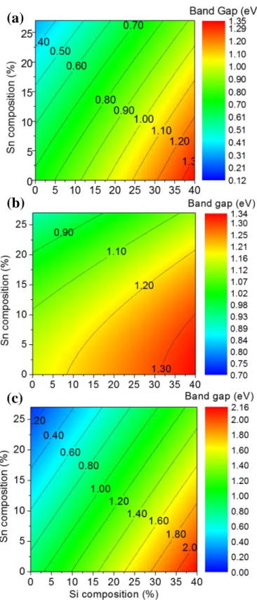
5.1 Band gap maps for strained and relaxed ternary alloy group IV semiconductors Ge 1-x-ySixSny 61 5.2 GeSiSn based nanowires heterostructures ... 62
CHAPTER 6 ARTICLE 3: EXTREME IR ABSORPTION IN GROUP IV -SIGESN
CORE-SHELL NANOWIRES ... 69
6.1 Experimental and Theoretical Details ... 70
6.1.1 Growth of Ge1-x-ySixSny samples ... 70
6.1.2 Structural and Optical Properties ... 71
6.1.3 Theoretical Calculations ... 73
6.2 Results and Discussion ... 74
6.3 Conclusion ... 92
CHAPTER 7 GENERAL DISCUSSION ... 93
CHAPTER 8 CONCLUSION AND RECOMMENDATION ... 94
8.1 Band gap engineering ... 94
8.2 Properties of charge carriers in Ge1-x-ySixSny NW heterostructures ... 95
8.3 Light absorption engineering in Ge1-x-ySixSny NW heterostructures ... 95
8.4 Future work ... 96
BIBLIOGRAPHY ... 102
LIST OF TABLES
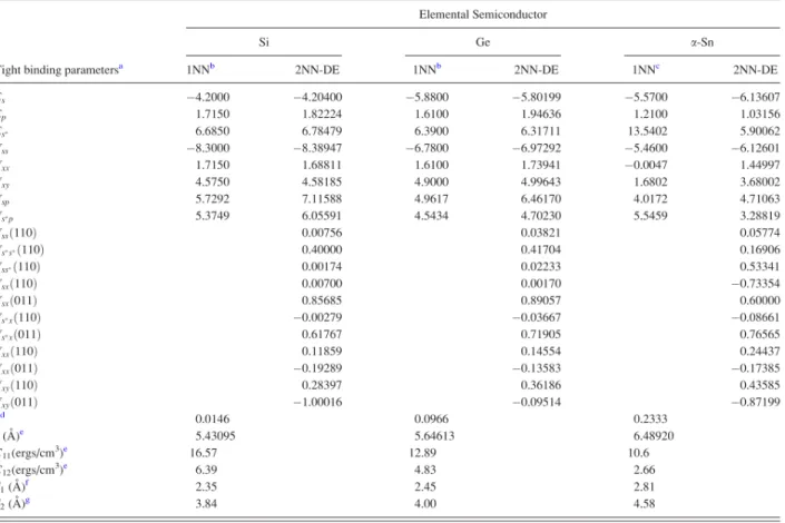
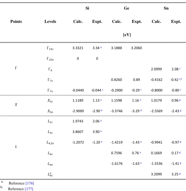
Table 4-1: Tight Binding Parameters in eV for the first nearest neighbor method (1NN-TBP) and second nearest neighbors approach (2NN-TBP) using differential evolution method for Si, Ge and α-Sn. ... 33 Table 4-2: Eigenvalues for diamond structure semiconductor at symmetry points Γ, X and L
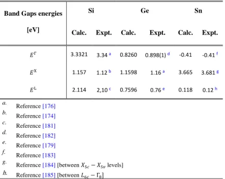
obtained from 2NN-sp3s* model and compared to experimental and non-local pseudopotential method.[175] ... 34 Table 4-3: Band gap transition energies of Ge, Si and α-Sn along highest symmetry axes 𝚪𝚪, 𝐋𝐋,
and 𝐗𝐗. ... 36 Table 4-4: Effective masses reproduced by the tight-binding parameters of Table 4-1 using the
differential evolution method. Masses are expressed in terms of electron mass. ... 36 Table 4-5: Comparison between experimental values of the band gap[188] and calculated band gap
based on the 2NN-sp3s* TB model (with and without the disorder contribution) model and the supercell mixed atom model.[155] ... 39 Table 4-6: The dimensionless scaling index ηmn used in the current calculations. ... 49 Table 4-7: The deformation-potential constants of Ge, Si and α-Sn. The column labeled ‘'theor’’
gives the values obtained by Van De Walle and Martin.[197] The column labeled MC show the stochastic Monte Carlo analysis performed in order to extract the DPC. ... 51 Table 4-8: Effect of strain on specific ternary alloy: three types of alloys are considered: a direct
(alloy I), direct-indirect crossover compositions (alloy II), and indirect (alloy III). Figure 4-3 show explicitly the evaluated composition. ... 54 Table 5-1: Material parameters used in our self-consistent calculations. 𝐸𝐸𝐸𝐸 is the band gap, Δ𝐸𝐸𝐸𝐸 is
the conduction band offset, 𝑚𝑚 ∗ is the relative electron effective mass which is taken from Ref. [49]. ... 64 Table 6-1: Core radius and shell thickness range corresponding to the optimal short-current
LIST OF FIGURES
Figure 2-1: Electronic band structures of Ge1−ySny for (a) y = 0.05, (b) y = 0.11, and (c) y = 0.20,
showing the transition from indirect [panel (a)] to direct bandgap [panel (c)] of Ge1−ySny.
Panel (b) illustrates the critical composition of 0.11, where the bandgap energies at L- and Γ-valleys are equal. The dashed line indicates the conduction band minimum (CBM) of Ge1−ySny. (After Ref.[49], reprinted with permission) ... 9
Figure 2-2: (a) The band structure of n-type Ge, and (b) a schematic diagram of the band gap reduction in L and Γ valleys with biaxial strain. (After Ref.[97], reprinted with permission) ... 10 Figure 2-3: Wavelength dependence of the absorption coefficient in cm-1 for several
semiconductors materials. (After Ref.[109], reprinted with permission) ... 12 Figure 2-4: (a) Schematic of GeSn/GeSiSn MQW LED. (b) Emission spectra at 4K and 300K of
d=100 µm GeSn/GeSiSn MQW (blue) and homojunction (dashed green) LEDs. ... 14 Figure 2-5: (a) Room-temperature photoluminescence of Ge1-x-ySixSny/Si samples with y>x. All
samples display emission peaks at longer wavelengths than the pure Ge emission at 1550 nm. (After Ref.[125], reprinted with permission) and (b) room-temperature photoreflectance spectra of unstrained Ge1-x-ySixSny sample with fixed Sn/Ge ratio about 0.069, but different Si
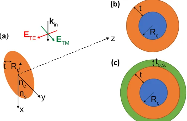
concentrations of 0%, 5,5% and 9.8 %. (After Ref.[121], reprinted with permission) ... 16 Figure 3-1: (a) Schematic of the analytical solution of light interaction with an infinite cylindrical
core-shell nanowire. The core and the shell are both formed with group IV semiconductor binary or ternary alloy having respectively different complex refractive index nc and ns. Cross-section of a cylindrical (b) CSNW system with a core radius 𝑅𝑅𝑅𝑅 and a shell thickness 𝑡𝑡 and a cylindrical (c) core-multishell nanowire system having a core radius 𝑅𝑅𝑅𝑅, an inner-shell of thickness 𝑡𝑡 and an outer-shell thickness 𝑡𝑡𝑡𝑡. 𝑠𝑠. with the respective complex refractive indices 𝑛𝑛𝑅𝑅, 𝑛𝑛𝑠𝑠. and 𝑛𝑛𝑡𝑡. 𝑠𝑠.. The material composing the outer-shell in panel (c) will either be a non-absorbing dielectric or GeSiSn semiconductor. ... 22 Figure 3-2: Measurement principle of ellipsometry ... 25 Figure 3-3: The rotating-compensator optical configuration of the used ellipsometry instrument 26
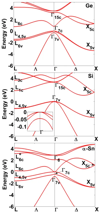
Figure 4-1: Bulk band structure obtained with 2NN-sp3s* ETB model for the elemental group semiconductors (a) Si, (b) Ge and (c) α-Sn using the parameters from Table 4-1. ... 38 Figure 4-2: Band structure maps of unstrained disordered ternary alloy Ge1-x-ySixSny through: (a)
L, (b) X and (c) Γ symmetry points. ... 40 Figure 4-3: Direct-Indirect Crossover of the unstrained Ge1-x-ySixSny ternary alloy. Two different
regions are distinguishable: The direct region and the L-indirect zones. The empty circles indicated are the selected alloys investigated in Figure 4-8. ... 42 Figure 4-4: Energy dependence of the Γ, Δ2, Δ4, L, and LH extrema for Ge as a function of the in-plane biaxial strain. The lines correspond to the results given by the tight binding formalism using the CGOM. ... 48 Figure 4-5: The value of the dilation Ξu + Ξd3 − aL deformation potential constant obtained from
the data set generated by Monte-Carlo simulations for Ge (a), Si (b), and α-Sn (c). ... 50 Figure 4-6: Strained band gap map of Ge1-x-ySixSny/ (001)Ge with disorder along (a) L and (b) Γ
symmetry points ... 53 Figure 4-7: (a) Band gap map of strained Ge1-x-ySixSny layer. The black solid line is the transition
between the tensile and compressive regions. The filled squares represent the crossover from direct to indirect for the strained ternary alloy and the corresponding equation is a linear fit in the (x, y) plane (S for strained alloy). However, the empty squares represent the direct to indirect transition line for the unstrained Ge1-x-ySixSny (R for relaxed alloys). The red line is
a linear fit for both type of crossover to extract the Y-intercept. Finally, the empty circles represent the transition in the indirect region from the L-symmetry point to the X-symmetry. (b) The strain map of the Ge1-x-ySixSny/ (001)Ge heterostructure as a function of Sn and Si
contents. ... 55 Figure 4-8: Band gap behavior as a function of strain along the symmetry points L, 𝛤𝛤 and X for 3
Ge1-x-ySixSny ternary alloys with: (a) (𝑥𝑥, 𝑦𝑦) = (4%, 21%), (b) (𝑥𝑥, 𝑦𝑦) = (4%, 15%) and
(c) (𝑥𝑥, 𝑦𝑦) = (10%, 15%) ... 56 Figure 4-9: Band gap map of GeSiSn/ (100)Ge system for a strain independent composition where
the Si and α-Sn compositions vary from 0 to 40% and 0 to 20% respectively and the strain values are equal to (a) 0.5% and (b) 1.0%. The red lines represent the relaxed direct to indirect
crossover, whereas the black continuous lines are the corresponding strained crossover lines. ... 58 Figure 5-1: (a) Dimensionless core-normalized variations of the electron density as a function of
the Ge0.9Sn0.1 core radius and doping density for a Ge shell of 20 nm. (b) This figure shows
the conduction band offset for a type I heterostructure. Note that for Sn composition below 11%, GeSn is an direct band gap semiconductor[40,147]. ... 66 Figure 5-2: Dimensionless core-normalized variations of the electron density as a function of the
Ge0.86Sn0.14 core radius and doping density of electron free carriers for a Ge shell of 20 nm.
The inset show the conduction band offset for a type I heterostructure. Note that for Sn composition above 11%, GeSn is an L-indirect band gap semiconductor ... 67 Figure 6-1: High Angle Annular Dark Field Scanning Transmission Electron Microscopy
(HAADF/STEM) image of Ge0.84Si0.12Sn0.04 (a) Ge0.84Si0.04Sn0.12 (b) layers grown on Ge
virtual substrates. Note the absence of dislocations or extended defects in the ternary layer or at the interface. The corresponding diffraction patterns measured at the interface are shown as inset figures in (a) and (b) confirming the high crystallinity as well as the absence of Sn precipitates. Low magnification HAADF/STEM images and EDX maps of Si, Ge, and Sn in Ge0.84Si0.12Sn0.04 (c) and Ge0.84Si0.04Sn0.12 (d) layers. ... 72
Figure 6-2: The complex refractive index constant 𝑁𝑁𝑁𝑁 spectra of (top) Ge1-ySny binary
semiconductor alloy as a function of wavelength for different Sn composition and (bottom) of Ge1-x-ySixSny ternary alloy as a function of wavelength for different Si and Sn composition
obtained from a spectroscopic ellipsometry measurement. The inset show the multilayer model used to extract the optical properties (section 3.2.3 of Chapter 3) ... 73 Figure 6-3: Photocurrent enhancement for a bilayer structure having film thicknesses between 1
and 200 nm where the first layer of thickness 𝑑𝑑1, shown in the inset is either Si or Ge layer and where the top thin layer of thickness 𝑑𝑑2 is either Ge0.88Sn0.12, Ge0.84Si0.04Sn0.12 or
Ge0.84Si0.12Sn0.04. The short-circuit current enhancement is evaluated for when 𝑑𝑑1 = 𝑑𝑑2. ... 75
Figure 6-4: Unpolarized absorption efficiency Qabs (top) and unpolarized scattering efficiency Qsca
(bottom) of Si/Ge0.88Sn0.12 CSNW surrounded by air as a function of the core radius 𝑅𝑅𝑅𝑅 and
comparison, SiNW absorption and scattering efficiencies are also shown. The three black-dashed lines indicate the selected radii: on-resonance (at 𝑅𝑅𝑅𝑅 = 8 𝑛𝑛𝑛𝑛) and off-resonance (at 𝑅𝑅𝑅𝑅 = 60 𝑛𝑛𝑛𝑛). ... 76 Figure 6-5: Unpolarized absorption efficiency Qabs (top) and unpolarized scattering efficiency Qsca
(bottom) of Ge/ Ge0.88Sn0.12 CSNW surrounded by air as a function of the core radius 𝑅𝑅𝑅𝑅 and
the incident light wavelength for two different shell thicknesses: 𝑡𝑡 = 𝑅𝑅𝑅𝑅4 and 𝑡𝑡 = 𝑅𝑅𝑅𝑅. For comparison, GeNW absorption and scattering efficiencies are also shown. ... 77 Figure 6-6: (a) 2D short-circuit photocurrent enhancement 𝜂𝜂𝜂𝜂𝑠𝑠𝑅𝑅 map as a function of the shell
thickness 𝑡𝑡 and the core radius 𝑅𝑅𝑅𝑅 for the CSNW structures: from top-left to bottom-right: Si/ Ge0.88Sn0.12, Si/ Ge0.84Si0.04Sn0.12, Ge/ Ge0.88Sn0.12 and Ge/ Ge0.84Si0.04Sn0.12. 𝜂𝜂𝜂𝜂𝑠𝑠𝑅𝑅 is equal to
the absorption efficiency of the CSNW structure divided by the one for the core NW with a radius of 𝑅𝑅𝑅𝑅 + 𝑡𝑡. The horizontal dashed lines represent 3 different shell thicknesses (line a→𝑡𝑡=3 nm; line b→𝑡𝑡=50 nm and line c→𝑡𝑡=100 nm) that will be analyzed more in detail in Figure 6-7. Additionally, we present in panel (b) a line profile of Si/ Ge0.88Sn0.12. CSNW 2D
map, along two shell thickness (𝑡𝑡 = 0.25, 1 × 𝑅𝑅𝑅𝑅) directions, shown as solid red and dashed-red lines respectively in panel (a). The dashed-red lines represent intensity profiles extracted from the 2D map in panel a following the directions 𝑡𝑡 = 𝑅𝑅𝑅𝑅 and 𝑡𝑡 = 𝑅𝑅𝑅𝑅4. We also present the short-current enhancement of thin-film structure for 2 different top-layer thickness (𝑑𝑑2 = 0.25𝑑𝑑1 and 𝑑𝑑2 = 𝑑𝑑1) for a Si/ Ge0.88Sn0.12 stack. The red arrows represent the peak core radius
positions attributed to LMR. ... 82 Figure 6-7: Integrated solar absorption Jsc (mA/cm2)as a function of the core radius of the CSNWs
consisting of absorbing group IV binary and ternary alloy semiconductors materials. The shell thickness is fixed to (a) 3 nm, (b) 50 nm and (c) 100 nm and plot the solar absorption as a function of the core radius for Si/ Ge0.88Sn0.12, Si/ Ge0.84Si0.04Sn0.12, Ge/ Ge0.88Sn0.12, Ge/
Ge0.84Si0.04Sn0.12, GeNW and SiNW structures. The GeNW and SiNW solar absorption are
presented for comparison sake, with a core radius equal to 𝑅𝑅𝑅𝑅 + 𝑡𝑡 for a fair comparison, to easily visualize the enhancement of light absorption in these structures. We also show the near electric field profile at the highest achievable short-current at a shell thickness of 3 nm and a core radius of 7 nm. We can infer from the profile distribution that the leaky fundamental mode is responsible for such a high short-current. ... 84
Figure 6-8: Extreme light absorption enhancement map as a function of the core radius and the incident light wavelength for the Si/Ge0.88Sn0.12 core-shell nanowire for different shell
thicknesses 𝑡𝑡= [0.25, 0.5, 0.75, 1] × 𝑅𝑅𝑅𝑅. ... 86 Figure 6-9: (a) The short-current enhancement map of the (Si/Ge0.88Sn0.12/Si3N4) system where the
inner-shell thickness was set to be equal to the core radius (𝑡𝑡𝑡𝑡. 𝑠𝑠. = 𝑅𝑅𝑅𝑅) and the dielectric capping layer thickness 𝐷𝐷 was varied from 1 to 200 nm. The top panel shows the relative maximum change of the short-current enhancement (max𝜂𝜂𝜂𝜂𝑠𝑠𝑅𝑅 in %) vs. the core radius, whereas the left panel represents the relative change of max𝜂𝜂𝜂𝜂𝑠𝑠𝑅𝑅 vs.𝐷𝐷. The relative change is evaluated using the following equation: 𝜂𝜂𝜂𝜂𝑠𝑠𝑅𝑅 − 1 × 100. The short-current enhancement was evaluated as the ratio of the short-current of the core-multishell nanowire to the short-current of the base CSNW (Si/GeSn) (𝜂𝜂𝜂𝜂𝑠𝑠𝑅𝑅 = 𝜂𝜂𝑠𝑠𝑅𝑅Si/GeSn/SiN𝜂𝜂𝑠𝑠𝑅𝑅𝐽𝐽𝑡𝑡/𝐺𝐺𝐺𝐺𝐽𝐽𝑛𝑛). The orange and green arrows in the top panel represent, respectively, the core radii 𝑅𝑅𝑅𝑅 equal to 13.6 and 78.2 nm, where 𝜂𝜂𝑠𝑠𝑅𝑅 is enhanced. Next, fixing 𝑅𝑅𝑅𝑅 to the previous radii, panel (b) and (c) show, a 2D map of the absorption efficiency 𝑄𝑄𝑄𝑄𝑄𝑄𝑠𝑠 as a function of the incident wavelength 𝑁𝑁 and the dielectric thickness 𝐷𝐷. ... 88 Figure 6-10: (a) TM-like mode absorption efficiency (𝑄𝑄𝑄𝑄𝑄𝑄𝑠𝑠𝑄𝑄𝑄𝑄) of the Si NW structure (red curve),
Si/ Ge0.88Sn0.12 CSNW structure (blue curve) and Si/ Ge0.88Sn0.12/ Si3N4 structure (green
curve), surrounded by air, for 2 different core radii: 𝑅𝑅𝑅𝑅 = 13.6 and 78 nm. The GeSn shell thickness was fixed to the core radius and the dielectric capping layer 𝐷𝐷 is chosen to be 33 and 45 nm, respectively for each core radius. The resonant peaks were labeled from 1 to 10 for the different structures. (b) Near field magnitude for the total TM-polarized Poynting vector 𝐒𝐒𝑄𝑄𝑄𝑄2.. ... 91 Figure 7-1: Cross-section illustration of a GeSn p-i-n WDPD ... 96 Figure 7-2: Schematic illustration of Group- IV 𝐺𝐺𝐺𝐺1 − 𝑥𝑥𝑛𝑛 − 𝑦𝑦𝑛𝑛𝐽𝐽𝑡𝑡𝑥𝑥𝑛𝑛𝐽𝐽𝑛𝑛𝑦𝑦𝑛𝑛𝑛𝑛/𝐺𝐺𝐺𝐺1 − 𝑥𝑥𝑛𝑛 − 𝑦𝑦𝑛𝑛𝐽𝐽𝑡𝑡𝑥𝑥𝑛𝑛𝐽𝐽𝑛𝑛𝑦𝑦𝑛𝑛𝑛𝑛 Superlattices ... 98 Figure 7-3: GeSiSn-based multi-junction solar cell with an optimal 1 eV sub-cell. ... 98 Figure 7-4: Direct band gap Ge0.9Sn0.1 QW with type-I band alignment and carrier confinement
LIST OF SYMBOLS
Symbol Description
Unit
𝑄𝑄 Optical band gap bowing parameter
𝐶𝐶𝑎𝑎𝑎𝑎𝑎𝑎 Absorption cross-section m2
𝐶𝐶𝑎𝑎𝑠𝑠𝑎𝑎 Scattering cross-section m2
𝑄𝑄𝑎𝑎𝑎𝑎𝑎𝑎𝑇𝑇𝑇𝑇(𝑇𝑇𝑇𝑇) Absorption efficiency for transverse electric (magnetic) 𝑄𝑄𝑎𝑎𝑠𝑠𝑎𝑎𝑇𝑇𝑇𝑇(𝑇𝑇𝑇𝑇) Scattering efficiency for transverse electric(magnetic) 𝑛𝑛 Refractive index
𝑛𝑛𝐷𝐷 n-type doping density cm-3
𝑛𝑛𝑠𝑠 Core refractive index
𝑛𝑛𝑎𝑎 Shell refractive index
λ Wavelength nm
λc Cutoff Wavelength nm
Rc Core radius nm
t Shell thickness nm
LIST OF ABBREVIATIONS
1D One-Dimensional
2D Two-Dimensional
1NN-sp3s* First-Nearest Neighbor sp3s* tight binding method 2NN-sp3s* Second-Nearest Neighbor sp3s* tight binding method ARC Anti-Reflective Coating
ASTM American Society for Testing Materials CSNW Core-Shell Nanowire
CBM Conduction Band Minimum DPC Deformation Potential Constants DFT Density Functional Theory
ETBP Empirical Tight Binding Parameters
Ge Germanium
GeNW Germanium Nanowire
Ge1-ySny Germanium-Tin binary alloy (0<y<1)
Ge1-x-ySixSny Germanium-Silicon-Tin ternary alloy
GFP Group- VI Photonics IRPD Infra-Red Photodetectors IT Information Technology
LCAO linear combination of atomic orbitals LMR Leaky Mode Resonance
MC Monte-Carlo
NIR Near-Infrared
NW Nanowire
OEIC Optoelectronic Integrated Circuits PIC Photonic Integrated Circuits SE Spectroscopic Ellipsometry
Si Silicon
SiNW Silicon Nanowire
SWIR Short-wavelength Infrared
Sn Tin
TE Transverse Electric TM Transverse Magnetic
VCA Virtual Crystal Approximation VBM Valance Band Maximum
LIST OF APPENDICES
Appendix A – Enhanced IR Light Absorption in Group IV-SiGeSn Core-Shell Nanowires ... 124 Appendix B – Publications related to this work ... 134
CHAPTER 1 INTRODUCTION
Through the years, the power consumption of the information technology (IT) kept on increasing mainly as a result of the exponential growth in internet traffic which passed in 2016 the zettabyte (1 ZB = 270 bytes) threshold and expected to increase nearly threefold over the next few years to reach the staggering figure of 25 GB per month per capita in 2020.[1] Additionally, networks required for the Internet of Everything and big data platforms will also show a significant growth from 4.9 billion machine-to-machine connections in 2015 to 12.2 billion by 2020.[1] This continuous evolution has been fueling an increasing demand for bandwidth and high-performance computing and signal processing while at the same time raising both technological and environmental concerns. This growing challenge is exacerbated by the driving paradigm of the IT industry which has always been “performance at low cost”. This approach faces another brick wall since the beginning of the past decade when fundamental thermal limits were reached by some integrated circuits (ICs), which are at the core of IT. As the transistor density has been increasing at Moore’s Law pace[2] and transistors are operated at higher frequency, the associated heat management has become a serious burden.[3] For instance, the electrical interconnect delay and power are some of the challenges that need to be addressed as devices scale down.[3] The scaling of electrical interconnections is limited by the physical properties of copper wires which suffers from heat dissipation via Joule effect. [4].
In addition to the scaling challenges, the need for enhanced performance also adds to the aforementioned burdens. For instance, while the input/output pad pitches will remain around 100 µm for IC chips, it is expected that the required line rate for inter-chip interconnect will exceed 40GB/s by 2020. So far, there is no solution to achieve this rate with electrical interconnects on a printed circuit board (PCB). Moreover, their high transmission loss on the PCB and reflections at connectors also limit the reach of electric wires at a high channel line rate. Due to this delay, the density of information that can be sent is limited in order to have good signal to noise ratio. The ITRS roadmap shows that the RC delay is expected to become significant, especially for global interconnects (long 𝐿𝐿).[5]
In addition to tackling the anticipated scientific and technological challenges, any progress in semiconductor industry must also integrate a variety of other aspects. The progress enabled by the semiconductor-based IT has been an undeniable development engine creating a myriad of new opportunities for society and the economy, but its backbone (the data center industry, networks, and devices) represents a significant environmental burden resulting in energy consumption. The continued expansion of the industry means that the energy use of data centers, networks, and end-user devices, and the associated emissions of greenhouse gases and other air pollutants, will continue to grow.[6] Although the exact energy intensity of data dissemination from a source to a number of users is still a matter of debate,[7,8] there is a general consensus that its energy footprint is prone to continue its rapid growth[7–11] to reach at least 22% of the global electricity supply by 2023.[10] To overcome these limitations, copper wires and low-k dielectrics are used on chips to reduce resistance and capacitance, and improve interconnect speed. There exist other possible physical approaches to improve heat dissipation, including cooling the chips and three-dimensional structures with vertical connections. But the underlying scaling issues and other physical problems are still outstanding challenges.
Recent potential solutions proposed to overcome the technological bottlenecks discussed above, have recognized optical interconnections via silicon (Si) photonic platforms (also know as Group IV photonics GFP) as the key paradigm to simultaneously tackle performance requirements and power challenges.[12–15] Indeed, the use of photons as the medium to detect, process, and transmit information will enable higher data rates and higher interconnection densities at lower system-level power dissipations.[16] In fact, optical interconnects have been progressively eliminating copper-based electrical ones in long-haul networks. The next natural step is to extend this trend to chip-to-chip and inter-chip communications. This is crucial to meet bandwidth demands, heat management, and energy efficiency across servers, boards, and on-chip. As compared to the traditional IRPD, the GFP materials bring serious advantages.
The best approach to integrate electronics and photonics remains an open issue. Some argue for the expedient option of putting electronics and photonics on separate chips. Others have shown that hybrid systems in the telecommunications industry, throughout the bonding of small group III-V devices to Si circuitry, is commercially viable to produce on chip-lasers, amplifiers, modulators, switches and detectors.[17] A third approach would be manufacturing totally monolithic
optoelectronic integrated circuits (OEICs).[18,19] The last approach is attractive because the process is seamless, and deals with homogeneous materials, since the group IV semiconductors are covalently bonded, and have similar chemical and physical properties. One specific benefit of mass-produced chips based on Silicon photonics, is that they offer a path to an extremely low, attojoules-per-bit energy cost for networks, and thus the potential to significantly reduce consumption of the energy that powers today’s Internet society.[20]
Emerging applications require operation of photonic integrated circuits, and OEICs within an extremely wide spectral region, ranging from visible to terahertz. The characteristics of group IV elements and alloys give Group-IV Photonics the capability for addressing that broad spectrum, including the near-, mid- and far infrared. To take advantage of opportunities in new applications, scientists now must engineer GFP chips that operate at wavelengths longer than 1.55 μm. Many technologies can harmonize, synergistically, with both electronics, and photonics; including plasmonics, photonic crystals, nano-electromechanics, microfluidics, biological-material attachments, and microwave photonics. An opportunity exists to obtain new system functionalities by combining these technologies on one chip, in a 3-D, multilayer approach.
However, despites the advantages mentioned above, group IV semiconductors (mainly Si and Ge) suffer from a fundamental issue: poor light absorption and emission.Si has rather poor optical properties due to its indirect band gap, and limited light absorption especially in the near-infrared region (NIR) and beyond, thus limiting the efficiency of Si-based photodetectors light emitting devices. Consequently, the need to find a light active material, compatible with silicon technology, active in the range above 2 μm is of paramount significance to the CMOS industry. In general, there exists three approaches to transform an indirect material to a direct one: strain engineering, n-type doping, and alloying. It has been reported that the direct gap of Ge can be tuned with tensile-strain which leads to a slightly larger absorption edge near 1.6 μm.[21–23]
In addition to IT, the aforementioned challenges also limit the progress in the smaller but increasingly important sector of infrared- (IR-) based sensing and imaging. The latter is central in numerous applications such as night vision, building inspection, predictive inspection, maintenance of industrial equipment, environmental monitoring surveillance, automotive and maritime safety, and fire-fighting. In the military, IR imaging is used for thermal weapon sight as well as vehicle and portable vision. Although IR imaging is becoming prevalent, the high production cost has
been a major obstacle in the development of high-resolution devices. For instance, despite their importance in a variety of applications, short-wave IR (SWIR) imagers are currently out of the reach of mainstream IR technologies.[24–30] Traditionally, intrinsic photon infrared photodetectors were mainly based on semiconductor materials such as group IV-VI compounds (lead salts: PbS,[31] PbSe,[32] and PbTe[33]), group II-VI alloy (mercury cadmium telluride HgCdTe[34]), and group III-V compounds (InGaAs, InAsSb, InSb, and InGaSb).[35] However, this class of infrared photodetectors (IRPDs) is undermined by some disadvantages. This includes the high cost and small array size of these detectors translates to an overall cost of a megapixel SWIR sensor exceeding tens of thousands of dollars.[36] This is a major limitation that prevents the broad use of SWIR technologies. Additionally, the IV-VI compounds are known to suffer from poor mechanical properties as well as large permittivity, even though they are low-gap materials and are well studied in literature. In addition, the main motivation behind the numerous attempts to replace the II-VI compounds (HgCdTe) is to circumvent material-related limitations. Among them is the weak Hg–Te bond, which results in bulk, surface, and interface instabilities. Moreover, HgCdTe is known to have non-uniformity over large area, as well as high cost in growth and processing.[34] Finally, the III-V alloys can be monolithically integrated, yet the large lattice mismatch during heteroepitaxy of these compounds renders it an undesirable candidate for industry.[37]
To overcome the limitation imposed by Si and Ge indirect bandgap, this project will focus on developing Si-compatible light sources by exploiting the emerging group IV semiconductors. A possible candidate for such materials are Germanium-Silicon-Tin ternary (Ge1-x-ySixSny where x
and y are respectively the Si and Sn atomic composition) and Germanium-Tin (Ge1-ySny where y is
the Sn composition) binary alloys. This provides more flexibility to independently engineer the bandgap and lattice parameter in a similar fashion to the more mature III-V semiconductors. Both theoretical modelling,[38–40] and experimental results[41–48] show that the electronic band structure of Ge can be tuned by varying the Sn composition. It is predicted that electron and hole effective masses of Ge1-ySny decreases with an increasing Sn composition.[49] This has motivated
the investigation of Ge1-ySny as a next-generation semiconducting material for high mobility
channel metal-oxide-semiconductor field effect transistors (MOSFETs) in the sub-7 nm technology nodes[50–52] and silicon-based photonic devices, e.g. infrared photodetectors,[53–58] and light-emitting devices.[59–63] However, the fact that SiGeSn semiconductors can be grown on Si wafers
is crucial to achieve scalable, cost-effective Si photonics. By tuning composition and strain in SiGeSn-based heterostructures and low-dimensional structures, we plan to implement light emitters and detectors targeting the technologically important SWIR range. This novel family of optoelectronic devices will benefit from the compatibility with complementary metal oxide semiconductor (CMOS) processing leading to a full exploitation of the current microelectronic and optoelectronic technologies thus allowing:
• Production in a high-volume Si wafer fab with repeatability, uniformity, and cost-effectiveness;
• Standard design flow making photonics design very similar to CMOS design with a library of elementary devices allowing the manipulation of light in the same way as electrical signals;
• Managing supply chain from wafers to final product including on-wafer testing for electrical and optical functionalities.
Furthermore, coupling light trapping schemes with the dimensionality of Ge1-x-ySixSny
material can lead to an increase in light absorption efficiency in IRPDs. In fact, tuning the dimensionality of the material is another promising approach to increase its absorption efficiency. Conventional light trapping techniques relies on surface texturing and/or antireflection coating.[64–66] Whereas, nanowire photonics, an emerging topic, is gaining traction in the material science community due to a better control and understanding of the growth processes involved. It also allows the investigation of light generation, propagation, detection, amplification, and modulation.[67] Nonetheless, elucidating the fundamental electronic and optical properties of the material is an important task that will pave the road to better implement it in different contexts, and application. Specifically, analyzing the effect of strain and alloying on the electronic structure of GeSiSn will guide research for a more targeted integration of the material in photodetectors for instance.
The main objective of this thesis is to provide the foundation to implement material systems for Si-compatible light sources and photodetectors. This thesis focuses on band structure engineering in Ge1-x-ySixSny semiconductors. Knowledge of the bandgap energy of Ge1-ySny alloys
with different amounts of strain is of paramount importance to design future optoelectronic devices based on these emerging semiconductors. Ge1-ySny/Ge1-x-ySixSny heterostructures are also
investigated in both thin film and nanowire structures. This document is organized in seven chapters. In Chapter 2, a literature review is presented to describe the current state-of-the-art of the field. Chapter 3 outlines the basics of spectroscopic ellipsometry process, and gives a theoretical description for how to accurately evaluate the electronic structure of Ge1-x-ySixSny semiconductors.
Likewise, the Mie- Lorentz scattering formalism will be developed to calculate light scattering and absorption efficiencies of group IV based nanowire structures. Chapter 4 elaborates on the evaluation of the unstrained and strained electronic structure of Ge1-x-ySixSny using the second
nearest neighbors empirical tight binding approach. Chapter 5 shows that it is possible to confine electron and hole in a radial nanowire Ge1-ySny/Ge1-x-ySixSny heterostructure, by accurately tuning
the geometric dimension of the structure and the doping concentration of carriers inside the core-shell nanowire structure. Chapter 6 discusses light scattering and absorption of group IV based core-shell nanowires. Finally, Chapter 7 ties these topics together with suggestions for future work.
CHAPTER 2 LITERATURE REVIEW
In 1982, Ge1-ySny binary alloys have been mentioned for the first time in literature as a possible
direct bandgap group IV semiconductor with unusually high carrier mobilities.[68] Ge1-ySny has
long been considered as a hypothetical alloy due to the low solid solubility of Sn in Ge.[69] Despite this limitation, early reports on the growth of monocrystalline Sn-rich alloys started emerging in early 1990s mainly based on solid-source molecular beam epitaxy (MBE).[70] However, the quality of the grown films was not good enough for device fabrication due to dislocation defect presence. Consequently, the interest in this family of semiconductors progressively faded away until late 2000’s when the development of stable precursors enabled the growth of device-quality Sn-containing group IV semiconductors using Chemical Vapor Deposition (CVD). The revived interest in this material system has been motivated by the ability to control of the growth kinetics using CVD-based processes, which yield high-quality monocrystalline Ge1-ySny binary and Ge 1-x-ySixSny ternary alloys layers.[70] The availability of monocrystalline layers and heterostructures
raised pressing needs to understand their fundamental properties and their behavior as a function of strain and composition. This led to a surge in experimental and theoretical studies of the electronic and optical properties of these materials. In the following, the current understanding of the electronic structure and optical properties for binary and ternary alloys are presented.
2.1 Binary semiconductors Ge
1-ySn
yGe1-ySny semiconductors have been attracting a great interest in recent years as they provide a
reliable path to achieve Si-compatible optoelectronics. Diamond cubic tin (Sn in its alpha phase, α-Sn, or grey-tin) is a semimetal with a conduction band minimum at the Γ point sitting 0.41 eV below the valence band. By alloying Sn and Ge, the conduction band extrema at both L and Γ valleys are predicted to decrease in energy with increasing Sn composition. However, the Γ valley is predicted to decrease more rapidly than the L valley as shown in Figure 2-1. The basic properties of Ge1-ySny have been evaluated using a variety of theoretical approaches. This includes empirical
pseudopotential method,[38,49,71,72] the 𝑘𝑘. 𝑝𝑝 method,[73] tight-binding,[40,74] and density functional theory (DFT)[43,75–80] in virtual crystal approximation (VCA). Ge1-ySny is predicted
to undergo an indirect-to-direct transition around 6% Sn with a direct bandgap energy of 0.66 eV. In addition to theoretical studies, experimental investigations of the optical and electronic properties of Ge1-ySny have also surged in recent years as a result of the progress in the epitaxial
growth of Sn-rich films and heterostructures.[41,42,45,46,81–87] It is, however, important to note that strong discrepancies are found when comparing different studies currently available in literature. This mainly concerns the large bowing parameter of the direct band gap, the critical composition at which the direct gap is achieved, the dependence of the energy gaps on the atomic distribution, and the band offsets in the alloy.
2.1.1 Bowing parameter and critical composition
First, a broad range of values has been reported for the optical band gap bowing parameter, b. First principle calculations gave b of 2.06,[88] 2.75,[43] 2.49,[78] and 1.90,[89] while experimental works based on the spectroscopic techniques generally give a smaller optical band gap bowing of 0.94,[90] 0.25,[91] -0.4,[92] and 0.30.[93] The discrepancy between the band structure calculations and the experimental results has been attributed to the bowing of the bandgap produced by local distortions in the bond lengths and bond angles of the crystal. With the bowing effect, the composition-dependent bandgap energy of alloys can be expressed as a second order approximation
𝐸𝐸𝑔𝑔�𝐺𝐺𝐺𝐺1−𝑦𝑦𝐽𝐽𝑛𝑛𝑦𝑦� = 𝑦𝑦𝐸𝐸𝑔𝑔(𝐽𝐽𝑛𝑛) + (1 − 𝑦𝑦)𝐸𝐸𝑔𝑔(𝐺𝐺𝐺𝐺) + 𝑄𝑄𝑦𝑦(1 − 𝑦𝑦)
where 𝐸𝐸𝑔𝑔(𝐽𝐽𝑛𝑛) and 𝐸𝐸𝑔𝑔(𝐽𝐽𝑛𝑛) are the band gap energy for bulk Sn and Ge, respectively.
Second, the critical composition (yc) at which the band structure transits from indirect to direct gap
is still not accurately established for relaxed and strained Ge1-ySny alloys. Low et al. reported a
critical composition of 11% Sn using Empirical Pseudopotential Method (EPM) as shown in Figure 2-1. Eg,L and Eg,Г are the bandgap energies at the L- and Г-symmetry direction, respectively. Similar
to Ge, Ge0.95Sn0.05 [Figure 2-1(a)] is an indirect bandgap material, as the conduction band minimum
(CBM) is located at the L-valley. With increasing x, both Eg,L and Eg,Г shrink, but the latter shrinks
faster. Thus, Ge1-ySny becomes a direct bandgap material when y exceeds a critical yc = 0.11, as
shown in Figure 2-1(c).[49] There are several theoretical studies predicting Sn concentrations between 6.3 at.% and >20 at.% needed for the indirect-to-direct band gap transition.[78,94,95] For
relaxed Ge1-ySny layers, except for some isolated cases of extreme values of 1.6%[80] or 17%[78],
most of the available data from both experimental [45,86] and theoretical [38,39,43, 96] studies remain in a lower range of 4.5-8 at.%. Whereas research for strained materials consistently shows higher values for yc of over 8%, 10% , and between 10-13%.[39,81,85] This behavior is expected
and has been studied theoretically[39] and experimentally in [45].
Thus, establishing accurately the critical composition of Ge1-ySny constitutes a necessary and
important step to understand the material system and evaluate its relevance for photonic and optoelectronic applications. This necessitates an accurate calculation of the electronic structure. Additionally, as already mentioned above, strain can play a fundamental role in shaping the band structure and must therefore be incorporated in the estimation the critical composition.
Figure 2-1: Electronic band structures of Ge1−ySny for (a) y = 0.05, (b) y = 0.11, and (c) y = 0.20, showing
the transition from indirect [panel (a)] to direct bandgap [panel (c)] of Ge1−ySny. Panel (b) illustrates the
critical composition of 0.11, where the bandgap energies at L- and Γ-valleys are equal. The dashed line
indicates the conduction band minimum (CBM) of Ge1−ySny. (After Ref.[49], reprinted with permission)
2.1.2 Strain effect on electronic structure
Expectedly, strain has significant effect on the band structure and optoelectronic properties of semiconductors. For instance, as shown in Figure 2-2, by applying biaxial tensile strain, both the direct and indirect band gaps shrink. However, the direct gap shrinks faster than the indirect band gap, thus the difference between these two valleys decreases. Consequently, with enough strain,
Ge, for example, can transform into a direct band gap material. The critical tensile strain has been predicted to be between 1.6% and 1.9%.[97,98] The approach relying on strain alone to induce direct gap in Ge necessitates the use of non-conventional fabrication and processing techniques such as suspended Ge membranes to achieve the large amount of tensile strain needed for indirect to direct band gap transition.[99,100] The observed effect of strain also emerges as an interesting strategy to achieve direct band GeSn semiconductors. Recent advances in non-equilibrium growth technique for GeSn have enabled the growth of GeSn semiconductors with alloy substitutional Sn content exceeding 16%.[101] Therefore, a combination of strain and Sn alloying, i.e., strained GeSn alloys may be able to relax the requirements on both the amount of Sn as well as the tensile strain needed to obtain a direct band gap.
In principle, biaxial tensile strain can be achieved by three different methods: thermal mismatch, mechanical stress, and lattice mismatch. First, thermal mismatch relies on the fact that thermal expansion coefficient for Si (2.6 × 10⁻⁶ °C-1) is half of the coefficient for Ge
0.955Sn0.045 (5.8 × 10⁻⁶ °C-1) which can generate a measured thermal strain of +0.34%.[102] Second,external stress
can be applied to designed GeSn Micro-Electro-Mechanical Systems (MEMS) structures.[103]
Four times larger strain can be achieved using this approach, compared to the maximum strain using the first method. Third, by epitaxially growing Ge1-ySny layers on a larger parameter lattice.
This approach is yet to be demonstrated. Note that the growth on Ge substrates yields compressively strained GeSn layers, which require a much higher amount of Sn to reach a direct band gap.[39,81,85]
Figure 2-2: (a) The band structure of n-type Ge, and (b) a schematic diagram of the band gap reduction in L and Γ valleys with biaxial strain. (After Ref.[97], reprinted with permission)
2.1.3 Band offsets
Little information can be found in literature concerning the band offset in Ge1-ySny, due to the
difficulty in establishing their values, as has been properly discussed in Ref.[43]. The authors report the natural valance band maximum (VBM) offset between Ge and Sn to be 0.91 eV, whereas the conduction band maximum (CBM) offset to be -0.41 eV. Additionally, the natural VBM and CBM (direct band) offsets between Ge and Sn has been calculated to be equal to 0.55 eV and -0.7 eV using DFT approach based on the Tran and Blaha MBJLDA functionals.[104] Furthermore, H-S. Lan et al.,[105] analyzed theoretically, using the nonlocal empirical pseudopotential method, the band structure of a p-type Ge cap/fully strained Ge1-ySny quantum well/ Ge (001) where they
reported a calculated valance band offset Δ𝐸𝐸𝑣𝑣 of ~80 meV in Ge0.95Sn0.05 by using the model solid
theory (MST)[106]. Their estimation was found to be within the reported measurement accuracy range of ±50 meV for y<0.08.[107] Establishing an accurate estimation of the natural band offset is vital from an application point of view. For instance, in heterostructures such as multi-quantum wells, the relative band positions in adjacent layers determine the character of carriers’ confinement, which in turn determines the type of the quantum well. We will address this issue in Chapter 5 by using the MST developed by Van de Walle[106] under the framework of the second nearest neighbors tight binding theory.
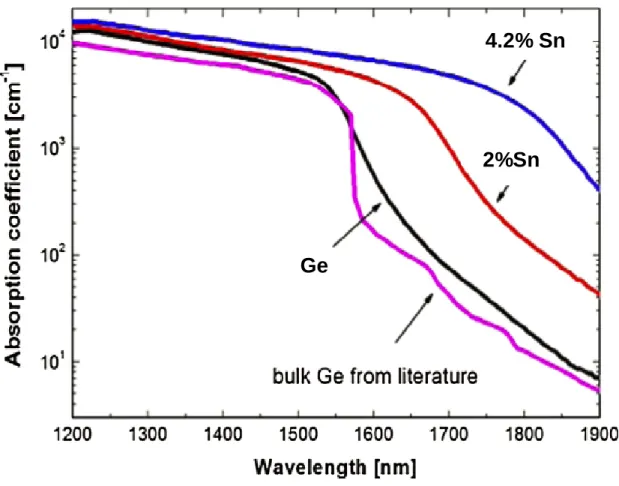
2.1.4 Enhanced light absorption of GeSn
The tunability of the GeSn band structure through Sn composition is an important advantage to implement optoelectronic devices operating in the NIR and MIR wavelength ranges. However, the use, for instance, of group IV photodetectors is limited by their relatively small range of efficient light absorption. Figure 2-3 shows the room-temperature absorption coefficient (α) versus light wavelength (λ) of Ge, and two GeSn samples with 2% and 4.6% Sn composition. This figure is replotted from Ref.[108] where V. D’Costa et al. measured room-temperature absorption coefficients of Ge1−ySny alloys with various Sn contents using spectroscopic ellipsometry. All the
Ge1−ySny films were fully compressively strained to the Ge (100) substrates. It can be observed that
an Sn composition of around 4.2% extends the absorption edge of Ge1−ySny into MIR region, and
the curves shift towards longer wavelengths with increasingly larger Sn composition.
Ge is almost transparent to photons with λ beyond 1.55 μm. The drastic decrease in the absorption coefficient in Ge, near λ = 1.55 µm, can be explained by the direct bandgap (near the Γ
symmetry point, denoted as 𝐸𝐸𝑔𝑔,Γ) of 0.8 eV. It can be observed that the higher the Sn composition, the more extended the absorption edge into the MIR region, will become. In other words, the absorption coefficient curves shift towards longer wavelength with increasingly larger Sn composition. This makes Ge1-ySny a very promising group IV semiconductor for NIR and MIR
photodetectors where adjusting the Sn composition can control the absorption properties. This is will be investigated in detail in Chapter 6.
Figure 2-3: Wavelength dependence of the absorption coefficient in cm-1 for several semiconductors
materials. (After Ref.[109], reprinted with permission)
2.2 Ge
1-x-ySi
xSn
yternary semiconductors
Modern semiconductor technology requires epitaxial layers with a precisely prescribed band gap and lattice constant. This dual requirement, which cannot be accommodated via “one-dimensional” binary AyB1-y (e.g. Ge1-ySny) or pseudo-binary AxB1-xC alloys, has motivated the quest for
“two-Ge
4.2% Sn
dimensional” ternary (AxByC1-x-y), pseudo-ternary (AxByC1-x-yD), or quaternary (AxB1-xCyD1-y)
materials whose band gaps and lattice constants can be tuned independently. Ternary group-IV alloys are the simplest semiconductors with a two-dimensional compositional space. Aside for Ge 1-x-ySixSny, the only other ternary group-IV semiconductors are those containing carbon, but these
can hardly be achieved experimentally due to the very small amounts of carbon that can be randomly incorporated in Si and Ge lattices.[110] In this thesis, the main focus is on the Ge 1-x-ySixSny system. Due to their compatibility with Si substrates, Ge1-x-ySixSny alloys can act as buffer
layers to control strain of device structures on Si substrates. Another special feature of Ge1-x-ySixSny
ternary alloys is the independent manipulation of both lattice constant and band structure. In other words, Ge1-x-ySixSny alloys have tunable bandgap energy at a fixed lattice constant. D’Costa et. al.
have grown Ge1-x-ySixSny alloys by reduced-pressure chemical vapor deposition (RP-CVD), and
they fixed the ratio of Si:Sn at 4:1 so that the Ge1-x-ySixSny alloys were lattice-matched to Ge.[111]
Using variable-angle spectroscopic ellipsometer, they observed an increased direct bandgap with increasing Si composition. Other optical transitions were studied in the same way.[112–114] By selecting the composition, the Ge1-x-ySixSny barrier layer can have the desired lattice constant to
strain or match the following Ge or Ge1-ySny QW layer, while keeping larger bandgap energy to
confine carriers inside the active Ge or Ge1-ySny layer. For instance, Chang et. al. proposed a
tensile-strained Ge laser based on a heavily n-type doped Ge/Si0.2Ge0.7Sn0.1 MQW structure.[115]
Strain-free Ge0.94Sn0.06/Si0.15Ge0.75Sn0.1 double heterostructures[116] and strain-balanced
Ge0.84Sn0.16/Si0.09Ge0.8Sn0.11 MQW lasers[117] were also proposed, and simulated for optical gain
as well. Type-I band offset alignment was assumed in these simulations. These simulations show promising results, but, due to limited experimental results, the material properties, such as bandgap energy and effective mass, used in the calculation are mostly based on theoretical predictions, which are fraught with large uncertainties. Moreover, LED device based on Ge0.915Sn0.085/Ge0.8Si0.1Sn0.1 MQW were fabricated, as schematically shown in Figure 2-4(a) and
yielded an emission peak position of 0.55 eV measured at 300 °C as shown in Figure 2-4(b). They also showed a great enhancement of the peak current density up to 130 A/cm2 compared to the GeSn homojunction.[118,119]
The accurate knowledge of the dependence of the band gap energy vs. composition and strain, as well as effectives masses, is necessary to the success of structure prediction and optimization. In earlier studies, Moontragoon et al. have used the charge self-consistent pseudopotential Xα
method[78], whereas Ventura et al. used tight-binding approach coupled with VCA[120] to calculate
Figure 2-4: (a) Schematic of GeSn/GeSiSn MQW LED. (b) Emission spectra at 4K and 300K of d=100 µm GeSn/GeSiSn MQW (blue) and homojunction (dashed green) LEDs.
the band structure of Ge1-x-ySixSny. The experimental characterization of the electronic structure of
Ge1-x-ySixSny alloys have been studied using optical and electro-optical methods. For instance, in
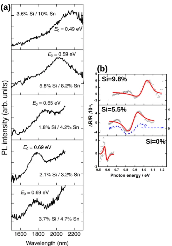
Figure 2-5(a), Xu et al. measured the photoluminescence spectra of multiple Ge1-x-ySixSny samples
grown on a Si substrate with a Sn concentration higher than the Si one (y>x). The direct gap emission peak 𝐸𝐸0 was measured and was estimated to follow a linear expression of the form 𝐸𝐸0(𝑥𝑥, 𝑦𝑦) = (0.785 ± 0.013) + (2.41 ± 0.11)𝑥𝑥 − (4.06 ± 0.19)𝑦𝑦 [𝐺𝐺𝑒𝑒].
(a)
Additionally, photoreflectance was used to measure the direct gap energy of unstrained Ge 1-x-ySixSny samples. Figure 2-5 shows that increasing Si composition for a fixed Sn/Ge ratio of 0.069
induces a blue shift for band gap.[121] Furthermore, the strong direct transitions were investigated using spectroscopic ellipsometry.[113,114,122] The lowest direct band gap was measured using spectroscopic ellipsometry,[113] photocurrent experiments in diode structures,[123,124]
photoreflectance,[121] and photoluminescence (PL).[125] Additionally, the fundamental band gap was determined using photoluminescence spectroscopy for Si and Sn compositions varying respectively from 2.4 at.% to 4.3 at.% and from 5 at.% to 8.1 at.%.[126]
Finally, it is important to note that establishing an accurate, non-computationally expensive methodology for studying the electronic structure and the optical properties of Ge1-x-ySixSny
material system will lay the groundwork to engineer an Si-compatible direct gap semiconductor that is efficient by tuning the Sn and Si composition and the strain independently. An additional degree of freedom to tune and enhance and optoelectronic properties is size and morphology as it is addressed is this project by using nanowire heterostructures. The second nearest neighbour tight binding approach will be our method to evaluate the electronic structure of relaxed and strained Ge1-x-ySixSny to establish the direct-to-indirect critical composition. Besides, the bowing parameter
as well as the band-offset will be extracted and compared to available literature data. Whereas, Mie-Lorentz Scattering formalism will be used to quantify light absorption based on experimental parameters extracted from ellipsometry studies.
Figure 2-5: (a) Room-temperature photoluminescence of Ge1-x-ySixSny/Si samples with y>x. All samples
display emission peaks at longer wavelengths than the pure Ge emission at 1550 nm. (After Ref.[125],
reprinted with permission) and (b) room-temperature photoreflectance spectra of unstrained Ge1-x-ySixSny
sample with fixed Sn/Ge ratio about 0.069, but different Si concentrations of 0%, 5,5% and 9.8 %. (After Ref.[121], reprinted with permission)
(a)
(b)
Si=0%
Si=9.8%
CHAPTER 3 METHODOLOGY
The evaluation of the electronic band structure of Ge1-x-ySixSny is crucial to establish a more
accurate understanding of the optical and electronic properties of this emerging class of semiconductors. To this end, we have chosen to use the second nearest neighbor empirical tight binding method (ETBM) to calculate the band structure. This was motivated by a couple of reasons. First, using semi-empirical approaches is computationally less expensive than full first-principle theoretical techniques, such as Density Functional Theory (DFT). Second, ETBM allows for an accurate evaluation of the energy band gaps and effective masses at room temperature which are important for device design and performance optimization. It is also noteworthy that the introduction of empirical parameters allows a better control of the theoretical simulations. Moreover, we also investigated light absorption and scattering inside NW structures based on the Mie-Lorentz scattering formalism to elucidate the light-structure interaction. However, to determine the absorption of light by nanostructure using the Mie-Lorentz approach, it is crucial to measure the optical constant of the material in question. One of the quickest and most accurate technique for that, is spectroscopic ellipsometry (SE).
This chapter is divided into a theoretical section and an experimental section. In the former, we outline the theory behind ETBM and the Mie-Lorentz scattering approach. Next, the experimental section describes the spectroscopic ellipsometry on how it is used to extract the optical properties of the measured samples. We will provide details on the experimental setup and on data analysis to extract the dielectric constant or the complex refractive index. Finally, we will present the steps undertaken to measure the Ge1-x-ySixSny sample and evaluate the optical properties
from the optical model.
3.1 Theoretical Methods
3.1.1 Electronic structure calculations
In developing the tight binding approach for electrons in a solid, we start from the assumption that electrons are tightly bound to nuclei. Bringing atoms closer together, the separation of the atoms becomes comparable to the lattice parameter in solid leading to the overlap of their wave functions.
![Table 4-5: Comparison between experimental values of the band gap [188] and calculated band gap based](https://thumb-eu.123doks.com/thumbv2/123doknet/2323425.29632/61.918.154.761.364.744/table-comparison-experimental-values-band-calculated-band-based.webp)