HAL Id: hal-00077297
https://hal.archives-ouvertes.fr/hal-00077297
Submitted on 30 May 2006
HAL is a multi-disciplinary open access
archive for the deposit and dissemination of
sci-entific research documents, whether they are
pub-lished or not. The documents may come from
teaching and research institutions in France or
abroad, or from public or private research centers.
L’archive ouverte pluridisciplinaire HAL, est
destinée au dépôt et à la diffusion de documents
scientifiques de niveau recherche, publiés ou non,
émanant des établissements d’enseignement et de
recherche français ou étrangers, des laboratoires
publics ou privés.
High-level synthesis under I/O Timing and Memory
constraints
Philippe Coussy, Gwenolé Corre, Pierre Bomel, Eric Senn, Eric Martin
To cite this version:
Philippe Coussy, Gwenolé Corre, Pierre Bomel, Eric Senn, Eric Martin. High-level synthesis under
I/O Timing and Memory constraints. 2005, pp.680-683. �hal-00077297�
High-level synthesis under I/O Timing and
Memory constraints
Philippe Coussy, Gwenole Corre, Pierre Bomel, Eric Senn, Eric Martin
LESTER LAB, UBS University, CNRS FRE 2734 Abstract—The design of complex Systems-on-Chips implies to
take into account communication and memory access constraints for the integration of dedicated hardware accelerator. In this paper, we present a methodology and a tool that allow the High-Level Synthesis of DSP algorithm, under both I/O timing and memory constraints. Based on formal models and a generic architecture, this tool helps the designer to find a reasonable trade-off between both the required I/O timing behavior and the internal memory access parallelism of the circuit. The interest of our approach is demonstrated on the case study of a FFT algorithm.
I. INTRODUCTION
Electronic design complexity has increased hugely since the birth of integrated circuits. System level technologies, over recent years, have moved from Application Specific Integrated Circuits (ASICs) and Application Specific Signal Processors (ASSPs) to complete System-On-Chip (SoC) designs. This increment in the chip complexity requires an equivalent shift in the design methodology and a more direct path from the functionality down to the silicon. In [1-3], the authors propose system synthesis approaches where the algorithms of the functional specification correspond to pre-designed components in a library. Macro generators produce the RTL architecture for hardware blocks by using the “generic”/ “generate” VHDL mechanisms: the synthesis process can hence be summarized as a block instantiation. However, though such components may be parameterizable, they rely on fixed architectural models with very restricted customization capabilities. This lack of flexibility in RTL blocks is especially true for both the communication unit, which I/O scheduling and/or I/O timing requirements are defined, and the memory unit, which data distribution is set.
High-Level Synthesis (HLS) can be used to reduce this lack of flexibility. For example, SystemC Compiler [4] from Synopsys, and Monet from Mentor Graphics, propose a set of I/O scheduling modes (cycle-fixed, superstate, free-floating) that allow to target alternative architectural solutions. Communication is specified using wait statements and is mixed with the computation specification what limits the flexibility of the input behavioral description. In these two tools, memory accesses are represented as multi-cycle operations in a Control and Data Flow Graph (CDFG). Memory vertices are scheduled as operative vertices by considering conflicts among data accesses. In practice, the number of nodes in their input specifications must be limited to obtain a realistic and satisfying architectural solution. This limitation is mainly due to the complexity of the algorithms that are used for the scheduling. Only a few works really schedule the memory accesses [5], [6]. They include precise temporal models of those accesses, and try to improve performances without considering the possibility of
simultaneous accesses that would ease the subsequent task of register and memory allocation.
In the domain of real-time and data-intensive applications, processing resources have to deal with ever growing data streams. The system/architecture design has therefore to focus on avoiding bottlenecks in the buses and I/O buffers for data-transfer, while reducing the cost of data storage and satisfying strict timing constraints and high-data rates. The methodology that can permit such a design must rely on (1) constraint modeling for both I/O timing and internal data memory, (2) constraint analysis for feasibility checking and (3) high-level synthesis.
In [7] and [8], we proposed a methodology for SoC design that is based on the re-using of algorithmic description. Our approach is based on high-level synthesis techniques under I/O timing constraints and aims to optimally design the corresponding component by taking into account the system integration constraints: the data rate, the technology, and I/O timing properties. In [9], we have introduced a new approach to take into account the memory architecture and the memory mapping in the behavioral synthesis of real-time VLSI circuits. A memory-mapping file was used to include those memory constraints in our HLS tool GAUT [10]. In this paper, we propose a design flow based on formal models that allow high-level synthesis under both I/O timing and memory constraints for digital signal processing algorithms. DSP systems designers specify the I/O timing, the computation latency, the memory distribution and the application’s data rate requirements that are the constraints for the synthesis of the hardware components. This paper is organized as follows: In section 2 we formulate the problem of synthesis under I/O timing and memory constraints. Section 3 presents the main steps of our approach, and its underlying formal models. In section 4, we demonstrate the efficiency of our approach with the didactic example of the Fast Fourier Transform (FFT).
II. PROBLEM FORMULATION
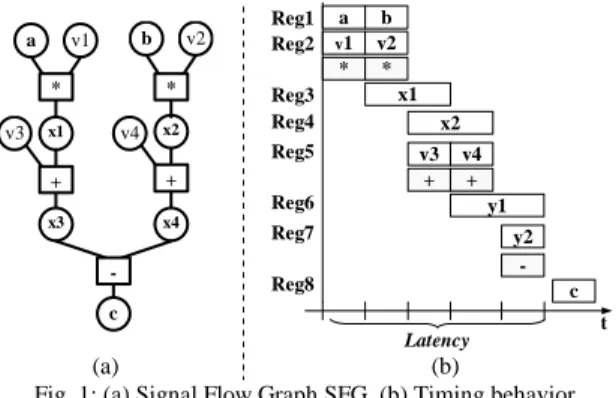
In this section, we illustrate the inter-dependency between the access parallelism to memory and the timing performances as well as the influence of these two parameters on the resulting component architecture. Let us consider a hardware component based on a generic architecture composed of two main functional units: one memory unit MU and one processing unit PU. Suppose the computation processed to be c = (a*v1 +
v3)-(b*v2+v4) where v1, v2, v3 and v4 are variables values stored in
memory. Fig. 1(a) shows the Signal Flow Graph (SFG) of this algorithm. This component receives input data a and b from the environment through an input port and sends its result c on the output port. All the data used and produced by the processing unit are respectively read and written in a fixed order
a v1 * x1 b v2 * x2 c v3 + x3 x4 v4 + -a Reg1 v1 Reg2 * x1 Reg3 b v2 y1 Reg4 + Reg5 * x2 c v3 + y2 v4 -Reg6 Reg7 Reg8 t Latency (a) (b)
Fig. 1: (a) Signal Flow Graph SFG, (b) Timing behavior, sequence S =(a,b,c): i.e. ta<tb< tc. The read sequence of two variables v1 and v2 is completely deterministic i.e.: tv1 < tv2. with
tv1 = ta and tv2 = tb. However, a scheduling choice is needed to access data v3 and v4 since a single memory bank is available in the component.
In our example, we choose to access v3 before v4. In this context, the minimum latency is therefore equal to 5 cycles (Fig. 1(b)). Fig. 2 presents a possible corresponding architecture of the processing unit that includes 1 multiplier, 1 adder, 1 substractor and 8 registers. Processing unit reg2 reg3 reg4 Memory Unit A B S reg1 * v1, v2, v3, v4 reg5 reg6 reg7 - reg8 +
Fig. 2: Sequential architecture
Let us now consider the following data transfer sequence
Sbusses = (a | b, c): i.e. ta=tb< tc. If the latency required to produce the result is long enough (≥ 5 cycles) to allow a reordering (serialization) of input data a and b, then the previously designed architecture including one memory bank can be reused. However, this solution need to design an input wrapper composed of 1 register, 1 multiplexer and 1 controller. If the required latency is not long enough (i.e. = 3 cycles), the designer must design a new component including 2 multipliers, 2 adders, 11 registers and 2 memory banks (see Fig. 3). In such a case, because of their restricted customization capabilities, neither a pre-designed component nor a macro generator would be flexible enough to respond to the new design constraints.
Processing unit reg2 + reg4 reg4 reg5 reg1 * reg12 reg11 * B C A reg3 reg5 + reg7 reg8 Memory Unit #1 Memory Unit #2 -v1 v3 v2 v4
Fig. 3: Parallel architecture
As stated before, a new design flow, based on synthesis under constraints, is needed to get flexibility and to make the DSP
component design easier. This includes (1) modeling styles to represent I/O timing and memory constraints, (2) analysis steps to check the feasibility of the constraints (3) methods and techniques for optimal synthesis.
III. DESIGN APPROACH OVERVIEW
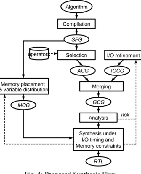
The input of our HLS tool [10] is an algorithmic description that specifies the functionality disregarding implementation details. This initial description is compiled to obtain an intermediate representation: the Signal Flow Graph SFG (see Fig. 4).
A. Timing Constraint Graph
In a first step, we generate an Algorithmic Constraint Graph
ACG from the operator latencies and the data dependencies
expressed in the SFG. The latencies of the operators are assigned to operation vertices of the ACG during the operator’s selection step in the behavioral synthesis flow. Starting from the system description and its architectural model, the integrator, for each bus or port that connects the component to others in the SoC, specifies I/O rates, data sequence orders and transfer timing information. We defined a formal model named IOCG (IO
Constraint Graph) that supports the expression of integration
constraints for each bus (id. port) of the component. Finally we generate a Global Constraint Graph (GCG) by merging the ACG with the IOCG graph. Merging is done by mapping the vertices and associated constraints of IOCG onto the input and output vertices set of ACG. A minimum timing constraint on output vertices (earliest date for data transfer) of the IOCG are transformed into the GCG in maximum timing constraints (latest date for data computation/production).
After having described the behavior of the component and the design constraints in a formal model, we analyze the feasibility between the application rate and the data dependencies of the algorithm, in function of the technological constraints. We analyze the I/O timing specifications according to the algorithmic ones: we check if the required constraints on output data are always verified with the behavior specified for input data. The entry point of the IP core design task is the global constraint graph GCG.
B. Memory Constraint Graph
As outlined in the previous subsection, A Signal Flow Graph (SFG) is first generated from the algorithmic specification. A Memory Constraint Graph is a cyclic directed polar graph
MCG(V',E',W') where V'={v'0,..., v'n} is the set of data vertices
placed in memory. A memory Constraint Graph contains
|V'|=n+1 vertices which represent the memory size, in term of
memory elements. The set of edges E'=(v'i, v'j) represents possible consecutive memory accesses, and W' is a function that represents the access delay between two data nodes. W' has only two possible values: Wseq (sequential) for an adjacent memory access in memory, or Wrand (randomize) for a non adjacent memory access. In our approach, this SFG is parsed and a memory table is created. All data vertices are extracted from the
SFG to construct the memory table. The designer can choose the
data to be placed in memory and defines a memory mapping. For every memory in the memory table, we construct a weighted Memory Constraint Graph (MCG). It represents conflicts and scheduling possibilities between all nodes placed in this memory. The MCG is constructed from the SFG and the memory mapping file. It will be used during the scheduling process.
Algorithm Compilation SFG Selection operators ACG Synthesis under I/O timing and Memory constraints Merging IOCG GCG Analysis Memory placement
& variable distribution
MCG
RTL
I/O refinement
nok
Fig. 4: Proposed Synthesis Flow
Fig. 6(b) shows a MCG for the presented example with one simple port memory bank. The variable data v1, v2, v3 and v4 are placed consecutively in one bank. Dotted edges represent
sequential accesses (two adjacent memory addresses) and plain
edges represent random accesses (non-adjacent addresses). Further information about the formal models and the memory design can be found in [7], [8], [9].
C. Scheduling under I/O and Memory Constraints
The classical “list scheduling” algorithm relies on heuristics in which ready operations (operations to be scheduled) are listed by priority order. In our tool, an early scheduling is performed on the GCG. In this scheduling, the priority function depends on the mobility criterion. For operations that have the same mobility, the priority is defined using the operation margin. Next, operations are scheduled and bind to operators (see Fig. 5). Scheduling_Function
1) Operation_Mobility_computing(GCG) 2) For (time = 0; time < End; time = time + t_cycle) 3) List = Operation_Priority_listing(GCG)
4) Ready_Ops = Find_schedulable_operation(List, time) 5) Binding(Ready_Ops, operators_set, MCG, time) 6) End for
Binding Function
1) While (Ready_Ops!= NULL)
2) Ops_low_mobility = Get_first(Ready_Ops) 3) if(Op_low_mobility->margin > 0)
4) If(Find_mem_conflic(MCG, Ops_low_mobility) = FALSE) 5) If(operators_set != NULL)
6) Ops_Binding(sh_list, operator) 7) else //no opr or mem conflict
8) Posponed(Ops_low_mobility) 9) else // margin = 0
10) If(Find_mem_conflic(MCG, Ops_low_mobility) = FALSE) 11) Operator_cretation()
12) Ops_Binding(sh_list, operator) 13) else
14) Exit(cycle, operator, operation, memory bank, …) 15) end if
16) End while
Fig. 5: Pseudo code of the scheduling algorithm
An operation can be scheduled if the current cycle is greater than the ASAP time. Whenever two ready operations need to access the same resource (this is a so-called resource conflict), the operation with the lower mobility has the highest priority and is scheduled. The other is postponed. When the mobility is equal to
zero, one new operator is allocated to this operation. To perform a scheduling under memory constraint, we introduce memory access operators and add an accessibility criterion based on the
MCG. A memory has as much access operators as access ports.
The list of ready operations is still organised according to the mobility criterion, but all the operations that do not match the accessibility condition are removed from this list. Hence, when the mobility is equal to zero, the synthesis process exits and the designer have to target an alternative solution for the component architecture by reviewing the memory mapping and/or modifying some communication features.
Our scheduling technique is illustrated in Fig. 6 using the previously presented example where the timing constraints are now the following: S =(a|b,c) i.e. ta = tb < tc. The memory table (Fig. 6(a)) is extracted from the SFG and is used by the designer to define the memory mapping. Internal data v1, v2, v3 and v4 are respectively placed at address @0, @1, @2 and @3 in the bank0. Our tool constructs one Memory Constraint Graph MCG (Fig. 6(b)). In addition to the mapping constraint the designer also specifies two latency Lat1=5 cycles and Lat2=3cycles. For latency Lat1, the sequential access sequence is v1 → v2 →
v3 → v4 : it includes 3 dotted edges (with weight Wseq). To deal
with the memory bank access conflicts, we define a table of accesses for each port of a memory bank. In our example, the table has only one line for the single memory bank0. The table of memory access has Data_rate / Sequential_access_time elements. The value of each element of the table indicates if a memory access operator is idle or not at the current time (control step c_step). We use the MCG to produce a scheduling that permits to access the memory in burst mode. If two operations have the same priority ( margin = Lat1-T(+)-T(*) = 1 cycles) and request the same memory bank, the operation that is scheduled is the operation that involves an access at an address that follows the preceding access. For example, multiplication operation (a*v1) and (b*v2) have the same mobility. At c_step cs_1, they are both executable and the both operands v1 and v2 are stored in bank0.
MCG_1 indicates that the sequence v1 → v2 is shorter than v2
→ v1. We then schedule (a*v1) at c_step cs_1 and (b*v2) at c_step cs_2 to favour the sequential access (see Fig. 6 (c)). At c_step cs_3, addition (x1+v3) and (x2+v4) have the same mobility, the MCG indicates that sequence v2 → v3 is shorter than v2 → v4. Addition (x1+v3) is scheduled at c_step cs_3 and
(x2+v4) at c_step cs_3. Bank @ v1 0 0 v2 0 1 v3 0 2 v4 0 3 Bank @ v1 0 0 v2 0 1 v3 0 2 v4 0 3 v1 v3 v2 v4 v1 v3 v2 v4 b v2 a v1 c * + -* v3 + v4 x1 x2 (a)Memory Table (b) MCG (c) Scheduling
Fig. 6: Scheduling under I/O timing and latency constraint For latency Lat2, multiplication operation (a*v1) and (b*v2) have the same mobility that is null. Both operations must then be scheduled in c_step cs_1. Because of the memory access conflict, there is no solution to the scheduling problem: the designer has hence to review its design constraints. He can target an alternative solution by adding one memory bank or by increasing the computing latency.
IV. EXPERIMENTAL RESULTS
We described in the two previous sections our synthesis design flow and the scheduling under I/O timing and memory constraints. We present now the results of synthesis under constraints obtained using the HLS tool GAUT [10]. The algorithm used for this experience is a Fast Fourier Transform (FFT). This FFT reads 128 real input Xr(k) and produces the output Y(k) composed of two parts: one real Yr(k) and one imaginary Yi(k). The SFG includes 16897 edges and 8451 vertices. Several syntheses have been realized using a 200MHz clock frequency and a technological library in which the multiplier latency is 2 cycles and the latency of the adder and the subtractor is 1 cycle.
A. Experiment 1: Synthesis under I/O timing constraints
In this first experiment we synthesized the FFT component under I/O timing constraints and analyzed the requirements on memory banks. In order to generate a global constraint graph GCG, minimum and maximum timing constraints have been introduced between I/O vertices of the ACG graph using the IOCG model. The FFT latency is defined by a maximum timing constraint between the first input and the first output vertices. The specified latency (that is the shortest one according to the data dependencies and the operator latencies) corresponds to a 261 cycles delay. The FFT component is constrained to read one Xr sample and to produce one Y sample every cycle.
The resulting FFT component contains 20 multipliers, 8 adders and 10 subtractors (see Exp#1 at Table 1). 8 memory banks are required for those I/O timing constraints. However, the internal
coefficients are mapped in a non-linear scheme in memory. A large amount of memory bank is needed to get enough parallel accesses to reach the specified latency. Moreover, coefficients can possibly be located in multiple banks what requires the design of a complex memory unit.
B. Experiment 2: Synthesis under memory constraints
In this second experiment we synthesized a FFT component only under memory constraints. Only the maximal number of concurrent access to the memory banks limits the minimal latency. Thus, with a large amount of operators, a latency equal to the critical path delay of the SFG could be obtained. For this reason, we synthesized the FFT with the same number of operators than in the first experiment. Then, we analyzed the requirement on I/O ports and computation latency. The memory constraints are the following: 2 memory banks respecting a simple mapping constraint: the 128 real coefficient Wr in bank0 and the 128 imaginary coefficient Wi in bank1.
The shortest latency imposed by the memory mapping and the number of operators corresponds to a 215 cycles delay (Exp#2 at Table 1). This delay is shorter that the delay obtained in the previous experiment. This architecture requires 36 input busses and 14 outputs. However, a large amount of busses with
non-trivial data ordering (non-linear data index progression) is needed. If the environment imposes the exchange of data over a smaller number of I/O busses, a communication unit should be designed. This unit would be able to add extra latency to serialize data.
C. Experiment 3: Synthesis under I/O timing and memory constraints
In this last experiment, we synthesized the FFT component under both I/O timing and memory constraints. We kept the
memory mapping used for the second experiment and founded the shortest latency that allows to respect the I/O rates defined in the first experiment. The resulting architecture contains 17 multipliers, 8 adders and 10 subtractors (see Exp#3 at Table 1). It produces its first result after 343 cycles.
TABLE 1: SYNTHESIS RESULTS
Memory bank.
Input busses
Output
busses Sub. Add. Mult.
Latency
(in cycle)
Exp#1 8 1 2 10 8 20 261
Exp#2 2 36 14 10 8 20 215
Exp#3 2 1 1 10 8 17 343
Because of both the memory mapping and the I/O constraints, the latency is greater than in experiment 1 and 2. However, the architecture complexity is equivalent to the previous ones in term of operators. Hence, it appears that synthesis under both I/O timing and memory constraints allows to manage both the system’s communication and memory, while keeping a reasonable architecture complexity.
V. CONCLUSION
In this paper, a design methodology for DSP component under I/O timing and memory constraints is presented. This approach, that relies on constraints modeling, constraints analysis, and synthesis, helps the designer to efficiently implement complex applications. Experimental results in the DSP domain show the interest of the methodology and modeling, that allow tradeoffs between the latency, I/O rate and memory mapping. We are currently working on heuristic rules that could help the designer in exploring more easily different architectural solutions, while considering memory mapping and I/O timing requirements.
ACKNOWLEDGEMENTS
These works have been realized within the French RNRT Project ALIPTA. REFERENCES
[1] J. Ruiz-Amaya, and Al., “ MATLAB/SIMULINK-Based
High-Level Synthesis of Discrete-Time and Continuous-Time Σ∆ Modulators“, In Proc. of DATE 2004.
[2] L. Reyneri, F. Cucinotta, A. Serra, and L. Lavagno. “ A hardware/software co-design flow and IP library based on Simulink“, In Proc. of DAC, 2001.
[3] Codesimulink, http://polimage.polito.it/groups/codesimulink.html
[4] H. Ly, D. Knapp, R. Miller, and D. McMillen, “ Scheduling using behavioral templates,” in Proc. Design Automation
Conference DAC'95, June 1995
[5] N. Passos, and al, “ Multi-dimensional interleaving for time-and-memory design optimization “, in Proc. of ICCD, 1995 [6] A. Nicolau and S. Novack, “ Trailblazing a hierarchical approach to percolation scheduling,” in Proc. ICPP'93, 1993, [7] P. Coussy, A. Baganne, E. Martin, " Communication and Timing Constraints Analysis for IP Design and Integration", In Proc. of IFIP
WG 10.5 VLSI-SOC Conference, 2003.
[8] P. Coussy , D. Gnaedig, and al., “A Methodology for IP Integration into DSP SoC: A Case Study of a MAP Algorithm for Turbo Decoder”, In Proc. of ICASSP, 2004
[9] G. Corre, E. Senn, and al., “Memory accesses Management During High Level Synthesis”, In Proc. of CODES-ISSS, 2004. [10] GAUT - HLS Tool for DSP, http://lester.univ-ubs.fr:8080/