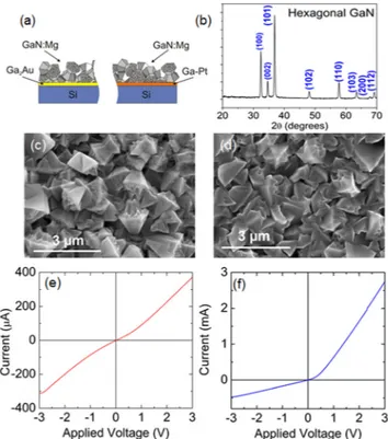
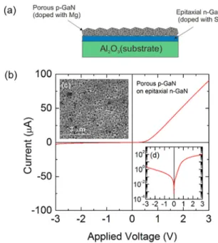
Fabrication of p-type porous GaN on silicon and epitaxial GaN
6
0
0
Texte intégral
Figure
Documents relatifs