Chemically resistant encapsulation for MEMS release
Serguei Stoukatch, Microsys, Université de Liège; Liege, BelgiumEster Tooten, ICTEAM, Université Catholique de Louvain; Louvain-La-Neuve, Belgium
Fabrice Axisa, Microsys, Université de Liège; Liege, Belgium Bruno Heusdens, TAIPRO Engineering, Seraing, Belgium
Laurent A. Francis, ICTEAM, Université Catholique de Louvain; Louvain-La-Neuve, Belgium
Jacques Destiné, EMMI, Université de Liège; Liege, Belgium
1 Introduction
Hence there is still lack of standardisation in MEMS fabrication technology, there are number features such technology, processes and material, those are common for different MEMS. The fabrication of MEMS [1] starts usually on silicon, or less often on glass wafer of common dimension used for conventional IC manufacturing [2]. State-of-the art MEMS are processed on 8” wafer, other factory and research institutions still utilize 3”, 4” and 6” facilities. The wafer is processed by basic technology used in IC fabrication such as material deposition and pattering definition. Many type of MEMS unlikely as a classic IC comprises moving parts (for instance: a silicon cantilever, a RF bridge, a membrane etc.). The moving parts are originally supported by a sacrificial layer that is typically an oxide. The last step of MEMS fabrication is a MEMS release. The MEMS release is etching away of the sacrificial material from the inside of MEMES structure, as a result of that the moving parts become released. The most common release etchant is based on HF (hydrofluoric acid), it is the HF acid aqueous solution of a different concentration and often mixed with other liquids such IPA (isopropanol) [3], methanol [4] etc. That is reportedly necessary to reduce and eliminate a stiction of the moving part, and ensures the clean and proper etching of the sacrificial layer. HF is used as an etchant for silicon dioxide, and it is an aqueous solution of 75% or 49% concentration, further diluted if necessary to 5:1, 10:1 or 20:1, is named as BHF (Buffered HF).
Till that point, namely the sacrificial layer etch, the MEMS device is robust enough to withstand any post-processing. After the MEMS release the device becomes vulnerable to any physical and chemical exposure. Such exposure can occur during transportation, handling or any post-processing (incl. the packaging). The vibration occurred during the transportation and handling, thermal exposure during post-processing and packaging, direct contact with liquid such water during dicing, direct mechanical contact with pick and place tool are just some factors that lead to damaging and destroying the moving part of the sensor. There are different approaches known to overcome such hurdles.
The first MEMS wafers [1] were first singulated on the individual dies, then they perform the release on individual devices. It makes process expensive and time consuming. It was suggested [1, 5] placing a cover over the wafer to protect the MEMS structures during the dicing process. In this case there is still work left at die
level to remove the covers. In case of capped MEMS, the cap can be placed first on the released wafer. The cap is to protect the MEMS during the singulation and packaging [6]. Dynatex [5] proposed another solution to this problem. The process comprises the wafer level MEMS release followed by a partial dicing saw cut across the entire wafer prior to the MEMS release step, while the wafer is still robust. Next, the MEMS process is completed and the MEMS are released. Finally, the wafer is transferred to the breaker for the singulation.
We have proposed and explored a novel sequence in MEMS fabrication process flow. The novel MEMS fabrication process flow can be shortly described as a “packaging first, MEMS release second”. We propose to package the MEMS device first (singulation, die mount, wire bonding and encapsulation) and to perform the MEMS release as the last step in the fabrication process flow. The main challenge we faced here is the encapsulation of MEMS device. The required encapsulant must withstand attack of the release etchant (HF acid).
This paper proceeds as follows. The MEMS features and manufacturing process flow are introduced briefly. Then the MEMS assembly process flow described in details. A special attention is paid for the encapsulation. In the following section we introduced the specification for the encapsulant material and we explained the selection criteria. Then, we describe the test method and the result of the test is demonstrated, in the last section we draw a conclusion.
2 MEMS features and manufacturing process flow
The novel MEMS fabrication process flow has been explored on a flow meter sensor. The sensor of 3mm x 3mm is fabricated on a silicon wafer at WinFab (UCL, Belgium). The sensor consists of movable 3-D (three-dimensional) bimorph cantilevers [3, 7]. The stimulus causes the deflection of the movable 3-D cantilever, the cantilever bends downwards or upwards respectively. A change in deflection is detected, transferred and converted into electrical signal and that is read-out.
Then the unreleased wafer is singulated on individual dies. The standard wafer singulation technique as a common sawing widely utilized in IC manufacturing was used for that. The sawing employs a high pressure water flow during the process, the water is necessary for cooling the dicing blade, for a sufficient friction and to remove silicone dust generated during the process out of the dicing kerf. The sawing is followed by the rinsing step that again employs a high pressure water flow, the rinsing is necessary to remove remains of the silicone dust generated during the process and deposited on the wafer surface. Typical parameters for the cutting water are pressure of 0.2-0.6 MPa and flow rate of 4-10 l/min. Because the sensors are still unreleased there is no damage observed on the sensor die despite the high pressure water flow applied on the wafer surface.
After sawing the wafer singulated on the individual MEMS devices is transferred to Microsys (ULG, Belgium) for the microassembly (or further in the text, described as packaging). Upon arrival, each individual dies was inspected and we did not detect any damage. Whereas the released wafer cannot withstand neither the sawing, nor the transportation cycle. The individual sensor (Fig.1) is mounted to the package. For the test purpose we used DIL24 package. DIL24 is a ceramic gold plated package. The package withstands the attack of the release solution (HF acid based).
Because the sensors are still unreleased the mounting becomes also not a critical process in the novel fabrication process flow. For the permanent fixation of the sensor to the package, we used EPOTEK H20E epoxy based adhesive. The epoxy was dispensed on the designed area of the package, the die was picked, aligned and placed onto the adhesive, then the assembly was cured within 15 min at 120°C in the convection oven, in N2 flow 5l/min. We also tested more commonly used adhesive for conventional IC packaging (60min curing at 150°C), the adhesive has no negative effect on the MEMS. Normally the die mounting process, as described above involving pick and place steps can cause a mechanical damage to the moving part of the sensor. If the sensor is released the standard die mounting process is usually impossible to use and in some case the hurdle can be overcome by utilizing special tooling. In our fabrication flow we used standard die mounting process that involved a direct top contact with the sensor die during pick and place steps. Also the unreleased sensor is less sensitive to the thermal exposure occurred during the adhesive curing step.
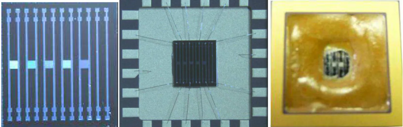
Fig. 1: From left to right: the singulated sensor die, the sensor die is mounted and wire-bonded to the DIL24 package, partially encapsulated sensor die.
Sequentially, we wire bonded the sensor. We interconnected the sensor die using Al wire bonding, it is a room temperature process. Al wire bonding is currently widely used for a special application (military, space etc). We also tested Au wire bonding (process temperature between 150-200°C) and we obse rved no damage on the sensor caused by the process.
To summarise up the MEMS manufacturing process flow, till now we utilize standard and commonly used in IC fabrication material, equipment and technology. That ensures process maturity, repeatability and high throughput, resulting in process low cost and low cost of process ownership. The last step of the assembly process flow is the encapsulation. However the choice for the encapsulant material is not evident.
3 Selection of encapsulant and encapsulation
The encapsulant must meet following specific criteria. First, the encapsulant must survive the chemical attack occurred during the MEMS release process. The release process is relatively harsh and combines a 10 min exposure to the release solution (mixture of 75%HF and IPA in 1:1 ratio), followed by a triple rinse of 5min each in a
rinsing solution (IPA). Normally, the encapsulant [8 attack of an aggressive chem
After the exposure to the release solution, it must be n degradation such as appearance of granular
inspection under microscope and SEM); inspection under microscope and SEM); mechanical strength (shear test).
must be resistant to the release solution, the material must serve the function of a partial encapsulation. It means that t
the package, and the intended part of the sensor die.
We performed an extensive literature search and contacted 10 different supplier manufactures on the encapsulant a
materials of different chemistry. considered encapsulant can resist
time. We had to set up an extensive test plan for that. Initially, based on some criteria’s out of 20 examined adhesives,
chemistry: a silicone-, an epoxy selected materials were app
silicon wafers and then sequentially
configurations that have different finish material deposited as following: Si/SiO2/Si3N4, Si/SiO2/ Si3N4/Al and Si/Si
dwelling the samples into the release solution and that all 6 tested materials withstand IPA.
the exposure to the release solution. The
criteria: there is no delamination, there is no texture change and the encapsulant maintains a sufficient mechanical adhesion.
assessed in terms of the
the initial value more than for 10 impact on the result of the
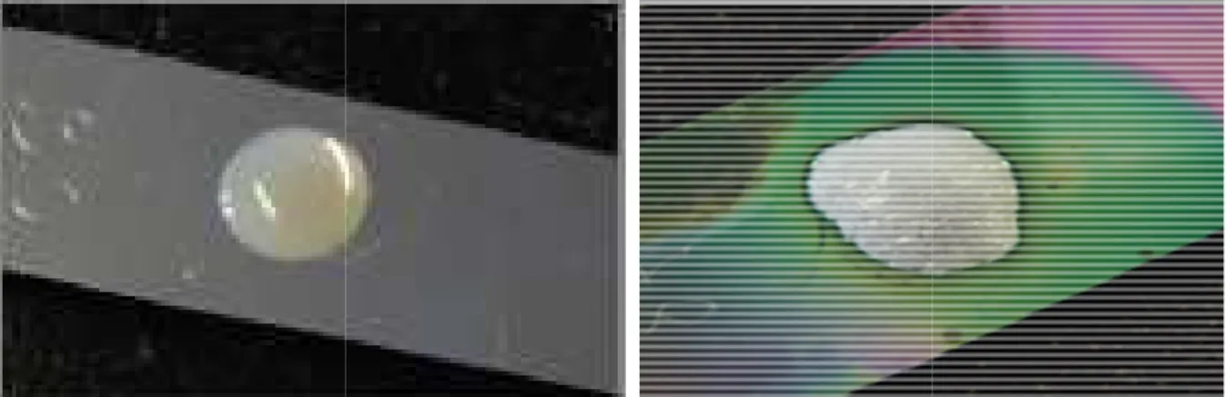
metal finish. On the other defects and irregularities texture turns to granular (F cracks occurrence.
Fig. 2: The encapsulant before release (left), and change texture to a granular du
A). Normally, the encapsulant [8] is not designed to withstand an chemical substance.
After the exposure to the release solution, it must be no any kind of the encapsulant appearance of granular structure, morphology and pits
inspection under microscope and SEM); no encapsulant delamination (visu inspection under microscope and SEM); and the encapsulant must m
mechanical strength (shear test). Additionally to the demand that the encapsulant the release solution, the material must serve the function of a means that the material must properly encapsulate the wire, the package, and the intended part of the sensor die.
extensive literature search and contacted 10 different supplier encapsulant and adhesive material. It total we examined 20 materials of different chemistry. It reveals us no or little hard
encapsulant can resist the attack of the 75%HF+IPA for 10 min
set up an extensive test plan for that. Initially, based on some criteria’s out of 20 examined adhesives, we pre-selected 6 encapsulants of different
, an epoxy- , a polyimide and an urethane
selected materials were applied in droplets of 5 mm diameter on cleaved then sequentially tested. We considered 4 dif have different finish material deposited as following:
Si/SiO2/Si3N4, Si/SiO2/ Si3N4/Al and Si/SiO2/Pd. The test comprises dipping and dwelling the samples into the release solution and followed by the rinsing
that all 6 tested materials withstand IPA. Whereas only two encapsulants
the exposure to the release solution. The 2 encapsulants passed the acceptance criteria: there is no delamination, there is no texture change and the encapsulant maintains a sufficient mechanical adhesion. The mechanical
the shear strength. The shear strength does
e initial value more than for 10%. We learnt that the finish metal has little or no impact on the result of the test; hence the encapsulant adheres differently to different
other 4 encapsulants that failed, we observed di
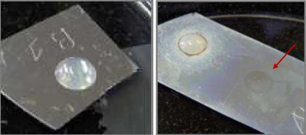
and irregularities induced by the release process: on some of them the texture turns to granular (Fig.2).We also observed a delamination (F
: The encapsulant before release (left), and after release ( change texture to a granular during the release.
] is not designed to withstand an any kind of the encapsulant structure, morphology and pits (visual encapsulant delamination (visual and the encapsulant must maintain sufficient Additionally to the demand that the encapsulant the release solution, the material must serve the function of a he material must properly encapsulate the wire, extensive literature search and contacted 10 different suppliers and It total we examined 20 or little hard data’s that any 75%HF+IPA for 10 min dwell set up an extensive test plan for that. Initially, based on some selected 6 encapsulants of different and an urethane-based. The pre-lied in droplets of 5 mm diameter on cleaved blanket
We considered 4 different wafer have different finish material deposited as following: Si/SiO2, The test comprises dipping and followed by the rinsing. We learnt encapsulants survives passed the acceptance criteria: there is no delamination, there is no texture change and the encapsulant The mechanical adhesion was trength. The shear strength does not deviate from We learnt that the finish metal has little or no hence the encapsulant adheres differently to different encapsulants that failed, we observed different type of : on some of them the o observed a delamination (Fig.3) and
Fig. 3: The encapsulant before release (left), and after release (right), the droplet (on the right part of the image) is peeled off during the release, whereas the droplet (on the left of the image) remains on the surface, hence delamination and microcracks are visible.
Fig. 4: The encapsulant before release (left), and after release (right), there is no difference observed.
The encapsulants (#1 and 2) that passed the acceptance criteria’s, are applied on the sensor die (Fig.5). The whole structure, the package and the assembled sensor is tested in the release and the rinse solution, and sequentially examined on presence of any damage. The observation is performed visually under the microscope with magnification of 100x. Additionally to that the SEM images (Fig. 6, 7, 8) at different magnification were taken.
Fig. 6: SEM image of the sensors: #1.1 right-top corner as marked by the arrow (left) and left-top corner as marked by the arrow #1.2 (right) after the release.
Fig. 7: SEM images reveal surface roughness (left) and crack formation (right).
The SEM inspection revealed different irregularities occurred on the rel
Fig. 7 (left), the SEM image taken at higher magnification (magnification of 500x) shows that the adhesive surface became rough and developed distinguishable morphology, the pits of 5
release was smooth and has no moreover some adhesive
the delamination of the adhesive out of the DIL package the DIL package surface and the encapsu
separation on the encapsulant from
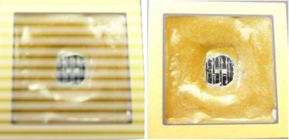
encapsulation the adhesive is thin, this is so encapsulated part and open part
Fig. 9: Partially encapsulated sensor
Fig. 10: SEM images reveal
The Fig. 10 shows the remains of t
originated during the release process, despite that we observed no irregularities occurred on the encapsulated part of the sensor
The SEM inspection revealed different irregularities occurred on the rel
, the SEM image taken at higher magnification (magnification of 500x) shows that the adhesive surface became rough and developed distinguishable orphology, the pits of 5-10µm are clearly seen. Whereas the surface before the
h and has no pits. On the Fig.7 (right) there is a moreover some adhesive peeled off. On the next image Fig.8 (left
the delamination of the adhesive out of the DIL package that seen as a gap between the DIL package surface and the encapsulation. On the Fig.
encapsulant from the silicone surface of the die, in that part of the encapsulation the adhesive is thin, this is so-called a transition area between encapsulated part and open part of the sensor. Then we tested the encapsulant #2.
: Partially encapsulated sensor # 2 before (left) and after the release
Fig. 10: SEM images reveal there is no irregularity.
s the remains of the release material, some dirt
originated during the release process, despite that we observed no irregularities occurred on the encapsulated part of the sensor #2. The adhesive
The SEM inspection revealed different irregularities occurred on the released sensor. , the SEM image taken at higher magnification (magnification of 500x) shows that the adhesive surface became rough and developed distinguishable 10µm are clearly seen. Whereas the surface before the there is a large crack and . On the next image Fig.8 (left) we documented that seen as a gap between lation. On the Fig. 8 (right), there is a the silicone surface of the die, in that part of the called a transition area between e tested the encapsulant #2.
the release (right).
he release material, some dirt and derbies originated during the release process, despite that we observed no irregularities e adhesive’s surface remains
smooth and the encapsulated part remains integral as before, there is no crack, delamination or other irregularities.
4 Conclusion
We have proposed and demonstrated a novel sequence in MEMS fabrication process flow. The novel MEMS fabrication process flow can be shortly described as a “packaging first, MEMS release second”. We propose to package the MEMS device first (die mount, wire bonding and encapsulation) and to perform the MEMS release as the last step in the fabrication process flow. The novel MEMS fabrication process flow has been demonstrated on a flow meter sensor. The sensor of 3mmx3mm is fabricated on a silicon wafer. The released wafer is singulated by sawing on individual dies, then the individual sensor is mounted to the package and wire-bonded. Because the sensors are still unreleased there is no damage observed caused by post-processing. The 6 encapsulants of different chemistry were tested and one of them survived the chemical attack of the release solution (75%HF:IPA=1:1).
5 Acknowledgments
The authors would like to acknowledge support from Microsys, ULG and DICE, UCL.
6 Reference
[1] R. Ghodssi, P. Lin. MEMS Materials and Processes Handbook. Berlin: Springer. (2011).
[2] Rao R. Tummala, Fundamentals of Microsystems Packaging. McGraw-Hill, (2001), 967 p.
[3] Nicolas André, Laurent A. Francis, Jean-Pierre Raskin, Philippe Nachtergaele, Jean-Marc Vaassen, Joe Civello, Sébastien Cases, Stéphane Paquay, Erwin De Baetselier. The Integrated Design of a MEMS-based Flow-Sensor System. Smart System Integration, Dresden 22-23 March 2011. Paper 35.
[4] Meltem Erdamar, Karthikeyan Shanmugasundaram, Paul Roman, Paul Mumbauer, Maria Klimkiewicz and Jerzy Ruzyllo, "Deep lateral anhydrous HF/methanol etching for MEMS release processes", J. Micro/Nanolith. MEMS MOEMS 7, 033014 (Jul 30, 2008); doi:10.1117/1.2959177.
[5] Application Note MEMS Singulation http://www.dynatex.com/images/ 7079749264.pdf
[6] Rottenberg, X.; Soussan, P.; Stoukatch, S.; Czarnecki, P.; Nauwelaers, B.; Carchon, G.; De Wolf, I.; De Raedt, W. and Tilmans, H. RF-MEMS technology platform for agile mobile and satellite communications, Proceedings of the European Microwave Conference - EuMC 2006, UK, Manchester
[7] N. André, B. Rue, G. Scheen, L.A. Francis, D. Flandre, J.-P. Raskin, Ultra low power 3-D flow meter in monolithic SOI technology. ECS Transactions, 35 (5), pp.319-324 (2011).
[8] James J. Licari, Dale W. Swanson, Adhesive Technology for Electronic Applications. (2005), 459 p.