OATAO is an open access repository that collects the work of Toulouse
researchers and makes it freely available over the web where possible
Any correspondence concerning this service should be sent
to the repository administrator:
[email protected]
This is an author’s version published in:
https://oatao.univ-toulouse.fr/
2 6117
To cite this version:
Mattio, Elodie and Lamadie, Fabrice and Rodriguez-Ruiz, Isaac and Cames, Beatrice and Charton, Sophie Photonic Lab-on-a-Chip analytical systems for nuclear applications: optical performance and UV–Vis–IR material characterization after chemical exposure and gamma irradiation. (2020) Journal of Radioanalytical and Nuclear Chemistry, 323 (2). 965-973. ISSN 0236-5731 .
Official URL:
https://doi.org/10.1007/s10967-019-06992-x
Photonic Lab-on-a-Chip analytical systems for nuclear applications:
optical performance and UV-Vis-lR material characterization
after chemical exposure and gamma irradiation
Elodie Mattio 1 • Fabrice Lamadie 1G>
·
Isaac Rodriguez-Ruiz 1•2 • Beatrice Cames 1 • Sophie Charton 1Abstract
The use of microfluidics technology and the miniaturization of analytical techniques is of high interest for the chemical and nuclear industries. In the latter, the reduction of effluents deriving from actinides concentration monitoring along R&D and pilot-scale purification processes is a permanent concern. lndeed, the extremely harsh operation conditions limit the imple mentation of standard analytical techniques and methodologies, and in this regard, the use of spectrophotometric techniques for effluents characterization becomes advantageous in terms of robustness, implementation and sensitivity at the microfluidic scale. In this work, we report a study of the effect of exposure to different chemicals used in hydrometallurgical processes, and to gamma radiation typical of the Plutonium and Uranium Refining by Extraction process, on the optical and structural properties of different polymeric materials commonly used for the fabrication of microfluidic and optofluidic systems. This study shows that low-cost castable and/or engravable materials (e.g. polydimethylsiloxane and poly-methyl methacrylate) are ideal for the study and development of Photonic Lab on a Chip systems that will be used in a nuclear environment. Graphie abstract
Keywords Opto/microfluidic · Photonic Lab-on-a-Chip · Materials resistance · Irradiation · Chemical exposure
igj Fabrice Lamadie [email protected]
2
CEA, DEN, DMRC, University of Montpellier, Marcoule, France
Present Address: Laboratoire de Génie Chimique - CNRS, UMR 5503, 4 Allée Emile Monso, Toulouse, France
Introduction
With the generalization of fully automated and intelligent processes, microfluidic devices are more than ever at the heart of R&D. In particular, they are a relevant solution for the growing analytical needs inherent in process-control, without multiplying the dedicated tirnes and volumes. How ever, while the design and manufacturing issues of chips
(assembly, connectors) are often mentioned in literature (see e.g. recent review of Mariet et al. [1]), materials issues, especially regarding chemical and radiation exposure, are less discussed [2, 3] as glass is frequently considered in these studies. Yet, hydrometallurgical processes in particu-lar, implement strong acids and organic solvents, which are likely to interact with the chips manufacturing materials. Additional radiation damage is also possible in the nuclear industry. While glass is maybe the more-chemically resistant transparent material, the development cost of the chips and their low mechanical strength are potentially detrimental to a serial application. As a result, possible replacement materi-als need to be considered and are here studied.
In a previous work, the relevance of polydimethylsilox-ane (PDMS) chips for Uranium (VI) concentration meas-urements by UV–Visible absorption on microliter volumes has been evidenced [4]. Following the promising results obtained, and in anticipation of a possible industrial imple-mentation of this micro-analysis, two questions related to the chip durability must be examined: (1) the resistance to chemicals, that is shared by many chemical industrial sec-tors, and (2) the resistance to irradiation, that is more spe-cific to nuclear applications.
PDMS is among the most used materials for microchip fabrication by the classical cast moulding technique [5]. A low cost fabrication process for the microfluidic moulds was recently compared to the conventional soft lithography one, which requires clean room infrastructure and hazardous chemicals, for the fabrication of moulds for PDMS opto-fluidic Photonic Lab-on-a-Chip platforms (PhLoCs) [6]. These platforms, monolithically integrating micro-optical elements, allow for the implementation of optical spectros-copy for analytical purposes, in the vicinity of a microfluidic structure [7]. The good optical properties presented by these low-cost devices open up promising perspectives for one-shot chips that could be e.g. a good option for analytical purpose. However, resistance to chemicals is not granted with PDMS structures [2], and radiation damages need to be further investigated. Thus in order to improve the com-ponents durability, and the chips versatility (especially for analytical purposes), a right choice on fabrication materials must be done.
In this regard, many other optically transparent polymers [8] are seen as interesting candidates. OSTEMER, a recent thiol-alkene-epoxy co-polymer allowing for cast molding chip production, has shown high resistance to chemicals, as e.g. those used in solvent extraction [9]. On the other hand, other common optically transparent materials like poly-methyl methacrylate (PMMA), Polycarbonate (PC) and polystyrene (PS) have also been widely used for chip fabrication by different manufacturing techniques [10]. Among these techniques, it is worth to mention not only the standard thermo-molding [11] or engraving techniques
(such as laser engraving and micro-milling [12]), but also the emerging additive fabrication processes applied in 3D print-ing technologies [13]: stereolithography, laminated object manufacturing and more recently fused deposition model-ling [14]. These processes allow the serial production and reproduction of complex structures [15] at different scales, and more particularly at very small scales, as microfluidic systems require.
In a previous work [4], preliminary tests have been made to observe the possible effects of gamma irradiation on PDMS and OSTEMER, two candidates for the realization of Uranium measurements chips. In this short communica-tion, the chemical and irradiation resistance of these two materials, as well as that of other possible candidates for the manufacture of PhLoCs, is further examined. In addition to a simple visual observation, that is sufficient to qualitatively evaluate the creation of defects and materials swelling, the precise evolution of the relevant optical properties is quanti-fied using post-exposure UV–Vis and IR measurements. In a second step, two chips dedicated to absorptiometric analyses [4] have been made in the two most cheap and widely used materials, PDMS and PMMA, and their robustness has been compared to a glass (fused silica) made chip, the reference material.
Materials and methods
Materials preparationOptically transparent PC, PMMA and PS sheets 1–1.1 mm thick, typically used for micro-systems fabrication by thermo-molding, laser engraving or micro-milling tech-niques, were purchased from commercial distributors. Two commercial polymers for microsystems prototyping by cast moulding were also considered: PDMS, used for decades in microfluidics and optofluidics fabrication, and the latter OSTEMER. PDMS (Sylgard 184 elastomer kit, supplied by Dow Corning, MI, USA) sheets 1 mm thick were fabricated by single-step casting on a mould fabricated by using a flat plastic container with optical quality walls as a substrate, and creating a well-controlled 1 mm gap by using 1 mm thick glass slides as spacers. Analogously, OSTEMER sheets 1 mm thick (OSTEMER 322 crystal clear, supplied by Mercene Labs, Sweden, in the form of a bi-component resin to be mixed before cross-linking) were fabricated using the same process, but this time using a flat PDMS sheet as a moulding substrate, to prevent OSTEMER adhesion [16]. Samples to be chemically-exposed or irradiated were prepared by cutting the purchased or fabricated sheets in 2 cm × 2 cm pieces. 13 samples, presumed identical, were prepared for each investigated material. In each series, one sample was left non-irradiated and non-exposed to chemical
products, in order to serve as reference, three were exposed to chemical environment, and the other nine were irradiated (see Table 1).
Chemical exposure
In order to examine their possible optical properties degra-dation and their structural integrity in operation, samples were exposed to 4 aggressive media commonly used in hydrometallurgical processes, and particularly in the nuclear waste recycling process PUREX:
• Concentrated nitric acid (HNO3 4M), used for lixiviation and dissolution steps;
• Hydrogenated tetra propylene, TPH, which is a typical diluent used in solvent extraction analogous to dodecane; • Isane, which is also a diluent in solvent extraction, as a
substitute to TPH;
• Tributylphosphate, TBP, which is the reference solvent in the PUREX process (Note: the actual process uses a dilution of 30% TBP and 70% TPH).
Samples of each material were fully immersed for 24 h in each media, subsequently rinsed with abundant water, and finally dried out at room temperature before their optical characterization.
Gamma irradiation
Samples were irradiated using a Cs-137 gamma irradiation equipment, with a total activity of 171.7 TBq. They were placed in a 20 locations basket, so that their individual loca-tion, and dose, are perfectly known. Moreover to prevent any dose rate effect, locations have been chosen in order to keep dose rate as constant as possible during irradiation (from 0.628 to 0.851 kGy/h, depending on the distance from the gamma source). They were individually removed from the irradiator at different times, leading to different and con-trolled exposure doses (see Table 1).
UV–Vis and IR characterization
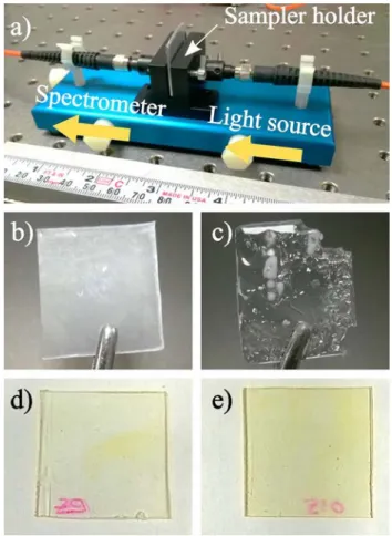
The UV–Vis transmission properties of all samples (ref-erence, chemically-exposed and irradiated) were studied by means of the setup described in Fig. 1a. The coupling of light to the samples was achieved using solarisation-resistant 400 µm fiber optics (Thorlabs, Newton, NJ, USA, NA = 0.22) directly connected to an ad-hoc fabricated sam-ple holder by means of collimation lenses, and allowing for
Table 1 Exposure doses versus
materials Material Exposure doses (kGy)
PC 6.3 20.0 26.0 39.7 45.4 59.1 65.7 78.6 87.5 PMMA 6.1 19.0 25.1 38.0 43.4 57.1 62.4 75.3 82.0 PS 5.8 18.1 23.9 35.4 40.5 54.4 59.3 72.0 81.1 PDMS 5.2 16.1 21.1 32.2 36.8 47.9 53.0 64.9 73.2 OSTEMER 5.1 15.5 20.7 31.4 35.9 47.1 51.0 62.8 64.5 Mean 5.7 17.7 23.3 35.3 40.4 53.1 58.3 70.7 77.7
Fig. 1 a Operation scheme and image of the experimental setup for UV–Vis sample characterization, b PMMA and c PS samples after 24 h immersion in TBP solvent, displaying surface etching and partial dissolution, d, e OSTEMER samples respectively irradiated at a dose of 58.81 and 60.48 kGy, displaying visible alteration of optical prop-erties (inhomogeneous yellowing). (Color figure online)
a correct and reproducible sample positioning. This sample holder is equipped with a slot (thickness gap 2 mm) that allows to set precisely the optical path (see Fig. 1a). A Ava-Light-D(H)-S-BAL balanced deuterium-halogen light source and a Avaspec ULS2048CL-EVO spectrometer (Avantes, Apeldoorn, Netherlands) were used for light coupling and subsequent spectrum analysis. Spectra were recorded from 200 to 1000 nm with a resolution of ± 0.56 nm fixed by the spectrometer in terms of pixel dispersion. Transmittance was classically calculated using the Beer-Lambert law. FTIR spectroscopy was performed on all irradiated and reference samples to characterize any possible sample chemical altera-tion caused by gamma irradiaaltera-tion degradaaltera-tion. To this end, a Thermo Nicolet FTIR 6700 was used, and spectra were collected in attenuated total reflection (ATR) mode. Analytical functional benchmark
The objective of this final test was to evaluate a potential influence of the material and the manufacturing process (laser engraving + chemical edging for high-resolution glass structures, micro-milling for PMMA and cast melding for PDMS) on the performance of UV–visible spectroscopic
measurements at the microfluidic scale. Thus, three geo-metrically identical chips have been manufactured, from the previously mentioned 3 different materials, based on the PhLoC design used in a previous work [4].
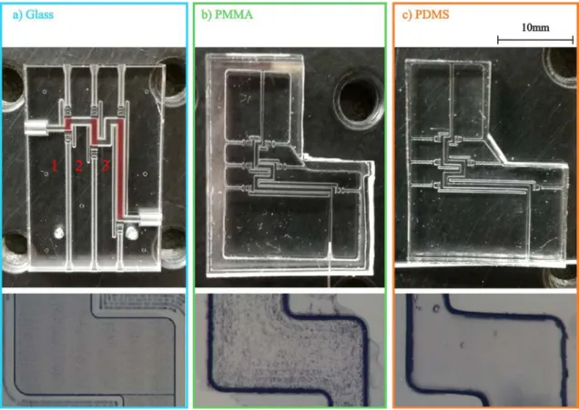
The first device was made of glass (cf. Fig. 2a), more precisely of fused silica with an OH content of 1200 ppm. It was manufactured by a special laser engraving + chemical edging technique developed by FEMTOprint (Switzerland). As fused silica is well-known for its excellent optical proper-ties, this chip was therefore chosen as the reference for com-parative purposes. A second chip was engraved in PMMA by micro-milling (cf. Fig. 2b), and third one was fabricated by casting PDMS on a dry film mould manufactured by soft lithography techniques [6] (cf. Fig. 2c). The common design for the 3 optofluidic chips consists of a fluidic continuous channel with three optical interrogation areas of increas-ing path length (highlighted in red in Fig. 2a). Each inter-rogation area comprised a set of collimating micro-lenses and auto-alignment channels, allowing for a correct posi-tioning of fiber optics (solarisation resistant fiber optics, 220 µm, Thorlabs, Newton, NJ, USA, NA = 0.22) on the microlenses focal point, in order to efficiently couple/decou-ple light to the system. Fiber optics were coucouple/decou-pled to the
Fig. 2 Upper part-Photographs of the three microfluidic chips (a glass, b PMMA, and c PDMS) used for comparisons (the 3 optical paths are highlighted in red on the glass chip). Bottom
part-Micro-scopic view of the 1 mm optical path on the three chips showing the differences in surface roughness. (Color figure online)
previously described light source and spectrometer, and the chips performances have been benchmarked in terms of light coupling efficiency and by absorptiometric measure-ments considering neodymium dosage. To this end, standard solutions of neodymium (III) nitrate hexahydrate (99.9%, Sigma-Aldrich, USA) in HNO3 (GPR RECTAPUR®, VWR Chemicals, USA) at 1 mol·L −1 have been prepared, in the range 0.1 ≤ C g·L−1 ≤ 50.
Results and discussion
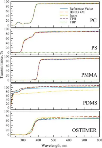
Chemical compatibilityFigure 3 compares the UV–Vis optical transmittance of the reference sample with samples of the same material after solvent exposure. For each material, almost identi-cal transmittance spectra were measured for the reference and the exposed samples. The variations observed for PDMS and OSTEMER samples are a consequence of the
manufacturing process leading to small thickness varia-tions, microbubbles occurrence, etc., locally modifying the optical properties of the material regardless the chemical exposure.
All samples displayed good structural resistance and preserved their optical properties when exposed to HNO3 4M. Regarding TPH exposure, only PDMS showed swell-ing, while no effect on transmittance spectra was observed. The other polymers were not affected by this solvent. For TBP exposure, PC, PDMS and OSTEMER remained stable after 24 h of total immersion, while the PMMA and PS samples were respectively partially (becoming opaque) or totally dissolved (see Fig. 1b, c). However, further tests performed on mixed TBP at 30% concentration in volume on TPH (common solvent in the PUREX process) revealed that both PMMA and PS remained unaltered after 24 h of immersion. Samples exposed to isane, displayed similar behaviour to those exposed to TPH (to be expected due to their close chemical composition), with a more pro-nounced swelling effect on PDMS, leading to a boost in size of about 30% (see Fig. 4).
This can be particularly detrimental for the structural stability of a microfluidic structure, especially considering the substantial changes in the optical path lengths in the case of absorptiometric PhLoC platforms. For the 1 mm thick samples considered, swelling was observed to result in a 10–25% decrease of transmittance on the UV–Vis spectra (depending on the wavelength). Moreover, due to the absorption of small molecules on the PDMS pores with coloured reagent, the use of isane or TPH solutions of coloured reagents leads to PDMS dyeing, which can directly influence the UV–Vis analysis. This last point may be an issue for the measurement of most of the elements involved in the PUREX process, particularly uranium and plutonium.
Fig. 3 UV–Vis transmittance spectra of reference and
solvent-exposed samples of the different polymers considered in this work. (Color figure online)
Fig. 4 PDMS before (left) and after 1 h immersion (right) in a solu-tion of yellow Sudan (4-phenylazo-1-phenyl-3-methyl-5-pyrazolone) at 100 mg L−1 diluted in TPH, showing evident swelling and dyeing
Effect of gamma irradiation
For each sample, 4 wavelengths, related to the maximum absorption peaks of Pu(III)—565 nm, Pu(IV)—475 nm, U(IV)—647 nm, and U(VI)—413 nm (of interest in the PUREX process for irradiated nuclear fuel treatment) have been selected, in order to assess the effects of gamma irra-diation in the polymers optical properties. The effect of increasing irradiation doses on the transmittance is illus-trated in Fig. 5 for each of the abovementioned wavelengths. Additionally, the full UV–Vis transmittance spectra measured on each samples are presented in Figures s1 to s5 of the supporting information. It can be observed that all materials presented barely noticeable to slight optical degradation above 500 nm at the wavelengths of interest, regardless of the irradiation dose (Fig. 5a, c). However, as we move towards the UV wavelengths, a significant effect of the dose level is observed: the higher the dose level, the higher the transmittance drop. This effect is less pronounced for PC, which is a plastic material widely used in nuclear environments, for manufacturing sealed containers such glove boxes or prototyping chemical reactors suitable to a radioactive surroundings. However it is especially notice-able for PMMA and OSTEMER (see trend lines depicted in Fig. 5b, d), which in addition exhibit a natural transmission cut-off in the near UV spectrum. In the case of OSTEMER, direct examination reveals inhomogeneous color formation, leading to yellowing zones, mainly at the higher irradiation doses (Fig. 1d, e). The observation of a red shift of the UV cut-off and the formation of an absorption tail, leading to polymer color formation is in agreement with previously reported data [17, 18]. Regarding OSTEMER, which is a heterogeneous material, the observed color inhomogenei-ties could be explained by an uneven distribution (due to insufficient reagent mixing) of the different monomers and additives within the samples, which are likely to promote radiation-induced color formation [19].
In order to evidence possible radiation effects on the poly-mers structural and chemical composition, FTIR absorbance
spectra were measured and are reported in Fig. 6 (the base-lines correspond to non-irradiated materials, i.e. the refer-ence value). All irradiated samples displayed (within the resolution of the spectrometer, < 1 cm−1) equivalent absorb-ance bands and peaks, without any deviation from the refer-ence samples. Thus, interestingly no irradiation effects could
Fig. 5 Optical transmittance properties for the irradi-ated samples, as a function of the dose, for the maxi-mum absorption peaks of a Pu(III)—565 nm, b Pu(IV)— 475 nm, c U(IV)—647 nm; and d U(VI)—413 nm, wavelengths of interest in the PUREX pro-cess for irradiated nuclear fuel treatment. (Color figure online)
Fig. 6 FTIR absorbance spectra, obtained in ATR mode, from each of the polymers of study irradiated at different exposure doses. (Color figure online)
be deduced from these analyses, even if some materials are obviously altered (see Fig. 1d).
To summarize, Table 2 condenses the results of irradia-tion and chemical exposure tests. In addiirradia-tion, the most com-mon manufacturing methods for each material are recalled to allow a more in-depth comparison. Corresponding data for fused silica are also reported for the sake of comparison, as it is today one of the preferred material for microfluidic devices, especially in hostile environment. While its resist-ance to chemicals is excellent, γ-irradiated fused silica dis-plays intense coloration (darkening), which is well reported in the literature [20, 21].
Functional benchmarking
We have observed that the exposure to γ-irradiation and chemicals of interest becomes limiting factors for the use of some of the studied polymers as construction materials for microfluidic/optofluidic chips to be used in a nuclear environment. But in order to assess microsystems optical quality (i.e. microsystems analytical performance), it is also important to account for the different chip fabrication tech-niques, which are strongly material-dependent. In this work we are benchmarking two widespread low-cost microfabri-cation techniques (micro milling and cast molding) against the highest optical standard for microfluidics microfabrica-tion at the present date (i.e. fused silica, providing standard optical material, and laser engraving + chemical edging, providing the best possible optical grade wall finishing to the microfluidic and micro-optical structures).
Figure 7a depicts the coupling efficiency of the three optofluidic systems, as a function of the optical path. Intensity values have been obtained by measuring the transmitted light through each system and optical path at 577.6 nm (absorption peak for neodymium dosage analy-sis) for a reference solution of HNO3 1M. Data has been normalized as a function of optical path length for compar-ison purposes. As expected, the light coupling efficiency is, in general terms, higher on the glass device compared
to the PMMA and PDMS systems. This effect is more evidenced at the 10 mm interrogation channels (which is actually 15 mm long on the glass chip), as the larg-est the optical path, the more critical becomes the optical quality of the micro optical elements to avoid undesired scattering and thus transmittance losses. Nevertheless, the coupling efficiency for the three systems is comparable. The resulting calibration curves for neodymium analytical dosage in acidic media, performed in the 3 different opto-fluidic chips, are compared in Fig. 7b. For each considered
Table 2 Summary of chemical and nuclear compatibilities of glass, OSTEMER, PC, PDMS, PMMA and PS (+ compatible, − deformation or
coloration of material, -- high degradation)
Compatibility Fused silica OSTEMER PC PDMS PMMA PS
Chemical exposure Nitric acid 4M + + + + + + TPH + + + − + + TBP + + + + -- --Isane + + + − + + Irradiation − [20, 21] − + + − +
Manufacturing Laser engraving Soft lithography Engraving, 3D printing,
Hot embossing Casting Engraving, 3D printing,Hot embossing Engrav-ing, Hot embossing Fig. 7 a Comparative of the light coupling efficiency through the 3 different interrogation channels for the glass, PMMA and PDMS optofluidic devices; b Calibration curves for neodymium analytical dosage in acidic media performed at λ = 577.6 nm on the 3 devices— (I) Optical path 10 mm (II) Optical path 1 mm. (Color figure online)
concentration, 5 measurements have been performed in order to assess the dispersion around the average values.
In each case, a linear evolution can be achieved using only 2 of the 3 available optical paths (1 and 10 mm), as highlighted in Fig. 7b. Moreover, the three chips reveal analogous sensitivity as the slopes of the adjusted linear regressions are comparable (see Table 3). In all three cases, the R2 ensures a good fit with the experimental data. Note that for the highest concentrations, it is theoretically required to account for the refraction effects induced by the solution and to correct the transmittance accordingly. However, for the sake of the comparison here considered, this effect can be neglected since it depends only on the sample optical path lengths (similar on the three chips) but not on the nature of the systems materials.
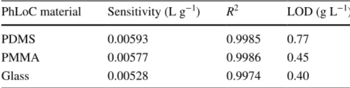
PMMA and glass exhibit a very close limit of detection (0.45 and 0.40 g·L−1 respectively), calculated here using the IUPAC definition [22]. According to this definition, LOD = k ⋅ sb∕m where k is a coverage factor ensuring a confidence level, m is the sensitivity defined as the slope of the linear fitting and sb is the standard deviation of the blank. It can be noted that the PDMS has a slightly higher detection limit of 0.77 g·L−1, due to a larger standard deviation of the blank and lower light coupling efficiency.
These results evidence that both PMMA and PDMS chips, although displaying a lower light coupling efficiency, exhibit analytical performances comparable to the reference fused silica chips for absorptiometric measurements. Fur-thermore, these two polymer materials are perfectly adapted for a Taylor made production of PhLocs with a lower cost.
Conclusions
Several polymeric materials used for the manufacturing of microfluidic chips have been investigated in view of their possible use in nuclear fuel reprocessing process: PDMS, PC, PS, PMMA and OSTEMER. The resistance to γ radia-tions, as well as to chemical products used in the PUREX process has been examined. For OSTEMER and PMMA, the direct visual observations reveal color changes after high dose of γ-irradiation. This effect, also reported for glass after following exposure to a few tens of kGy, is shared by most of transparent materials. As far as chemical compatibility is
concerned, PDMS, PMMA, and PS respectively displayed swelling and partial/total dissolution in presence of the sol-vents, and thus they are not suitable for microfluidic applica-tions involving organic solvents. They can however be used in an acidic environment and/or with time limited exposition to organic components. Besides these considerations, the manufacturing process itself must be considered, in terms cost and ease of fabrication of the chips: OSTEMER and PDMS chips, manufactured by cast molding, better fulfil these technical–economic criteria, as it does not require any specific and expensive equipment. The comparison between absorptiometric chips made of casted PDMS and engraved PMMA showed that the material and manufacturing pro-cesses has minor influence on the spectrophotometric meas-urements performances. The tests conducted here expose the materials to high doses of radiation or high TBP concentra-tion. They are hence quite penalizing tests and not neces-sarily representative of the process conditions. Additional studies are required in order to test the effects in more rep-resentative conditions, especially those induced by flowing radionuclides and/or diluted solvent.
Acknowledgements This work was supported by the Nuclear Energy
Division of CEA (DISN/PRATA-PRONG). IR-R acknowledges the CEA-Enhanced Eurotalents Program for his Incoming CEA post-doctoral fellowship.
References
1. Mariet C, Vansteene A, Losno M et al (2019) Microfluidics devices applied to radionuclides separation in acidic media for the nuclear fuel cycle. Micro Nanoeng. https ://doi.org/10.1016/j. mne.2019.02.006
2. Rodríguez-Ruiz I, Llobera A, Vila-Planas J et al (2013) Analysis of the structural integrity of SU-8-based optofluidic systems for small-molecule crystallization studies. Anal Chem. https ://doi. org/10.1021/ac402 019x
3. Piruska A, Nikcevic I, Lee SH et al (2005) The autofluorescence of plastic materials and chips measured under laser irradiation. Lab Chip. https ://doi.org/10.1039/b5082 88a
4. Rodríguez-Ruiz I, Lamadie F, Charton S (2018) Uranium(VI) on-chip microliter concentration measurements in a highly extended UV–visible absorbance linearity range. Anal Chem. https ://doi. org/10.1021/acs.analc hem.7b051 62
5. McDonald JC, Duffy DC, Anderson JR et al (2000) Fabrication of microfluidic systems in poly(dimethylsiloxane). Electrophor. https ://doi.org/10.1002/(SICI)1522-2683(20000 101)21:1%3c27:AID-ELPS2 7%3e3.0.CO;2-C
6. Rodríguez-Ruiz I, Teychené S, Van Pham N et al (2017) Broad-casting photonic lab on a chip concept through a low cost man-ufacturing approach. Talanta. https ://doi.org/10.1016/j.talan ta.2017.04.010
7. Rodríguez-Ruiz I, Ackermann TN, Muñoz-Berbel X, Llobera A (2016) Photonic lab-on-a-chip: integration of optical spectroscopy in microfluidic systems. Anal Chem. https ://doi.org/10.1021/acs. analc hem.6b003 77
8. Ren K, Zhou J, Wu H (2013) Materials for microfluidic chip fab-rication. Acc Chem Res. https ://doi.org/10.1021/ar300 314s
Table 3 Analytical features for the three chips (0–50 g·L−1,
measure-ments repeated 5 times)
PhLoC material Sensitivity (L g−1) R2 LOD (g L−1)
PDMS 0.00593 0.9985 0.77
PMMA 0.00577 0.9986 0.45
9. Carlborg CF, Moraga F, Saharil F, et al (2012) Rapid permanent hydrophilic and hydrophobic patterning of polymer surfaces via off-stoichiometry thiol-ene (OSTE) photografting. In: Micro Total Anal Syst (muTAS) 2012. Ginowan City Okinawa, pp 677–679 10. Ogończyk D, Węgrzyn J, Jankowski P et al (2010) Bonding of
microfluidic devices fabricated in polycarbonate. Lab Chip. https ://doi.org/10.1039/B9244 39E
11. Becker H, Gärtner C (2008) Polymer microfabrication technolo-gies for microfluidic systems. Anal Bioanal Chem. https ://doi. org/10.1007/s0021 6-007-1692-2
12. Guckenberger DJ, de Groot TE, Wan AMD et al (2015) Micromill-ing: a method for ultra-rapid prototyping of plastic microfluidic devices. Lab Chip. https ://doi.org/10.1039/C5LC0 0234F
13. Au AK, Huynh W, Horowitz LF, Folch A (2016) 3D-Printed microfluidics. Angew Chem Int Ed. https ://doi.org/10.1002/ anie.20150 4382
14. Bressan LP, Adamo CB, Quero RF et al (2019) A simple proce-dure to produce FDM-based 3D-printed microfluidic devices with an integrated PMMA optical window. Anal Methods. https ://doi. org/10.1039/C8AY0 2092B
15. Mattio E, Robert-Peillard F, Vassalo L et al (2018) 3D-printed lab-on-valve for fluorescent determination of cadmium and lead in water. Talanta. https ://doi.org/10.1016/j.talan ta.2018.02.051
16. Pham V (2016) Development of high throughput microfluidic plat-forms for the measurement of the protein solution thermodynamic properties
17. Moura EAB, Ortiz AV, Wiebeck H et al (2004) Effects of gamma radiation on commercial food packaging films—study of changes in UV/VIS spectra. Radiat Phys Chem. https ://doi.org/10.1016/j. radph ysche m.2004.05.034
18. Clough RL, Gillen KT, Malone GM, Wallace JS (1996) Color formation in irradiated polymers. Radiat Phys Chem. https ://doi. org/10.1016/0969-806X(96)00075 -8
19. Klemchuk PP (1993) Protecting polymers against dam-age from gamma radiation. Radiat Phys Chem. https ://doi. org/10.1016/0969-806X(93)90052 -V
20. Marshall CD, Speth JA, Payne SA (1997) Induced optical absorp-tion in gamma, neutron and ultraviolet irradiated fused quartz and silica. J Noncryst Solids. https ://doi.org/10.1016/S0022 -3093(96)00606 -0
21. Zhong M, Yang G, Yan Z et al (2016) Effect of γ-ray irradiation on the optical property and laser damage performance of silica. Optik. https ://doi.org/10.1016/j.ijleo .2016.01.065
22. Long GL, Winefordner JD (1983) Limit of detection: a closer look at the IUPAC definition. Anal Chem. https ://doi.org/10.1021/ ac002 58a00 1