HAL Id: hal-01184144
https://hal.archives-ouvertes.fr/hal-01184144
Submitted on 12 Aug 2015
HAL is a multi-disciplinary open access
archive for the deposit and dissemination of
sci-entific research documents, whether they are
pub-lished or not. The documents may come from
teaching and research institutions in France or
abroad, or from public or private research centers.
L’archive ouverte pluridisciplinaire HAL, est
destinée au dépôt et à la diffusion de documents
scientifiques de niveau recherche, publiés ou non,
émanant des établissements d’enseignement et de
recherche français ou étrangers, des laboratoires
publics ou privés.
Labelled OBS test bed for contention resolution study
Thomas Legrand, Hisao Nakajima, Paulette Gavignet, Bernard Cousin
To cite this version:
Thomas Legrand, Hisao Nakajima, Paulette Gavignet, Bernard Cousin. Labelled OBS test bed for
contention resolution study. 5th International Conference on Broadband Communications, Networks
and Systems (Broadnets 2008), Sep 2008, London, United Kingdom. pp.82 - 87,
�10.1109/BROAD-NETS.2008.4769048�. �hal-01184144�
Labelled OBS Test Bed for Contention Resolution Study
Thomas Legrand, Hisao Nakajima, Paulette Gavignet
France Telecom, Orange Labs R&D,
2 avenue Pierre-Marzin, F-22307 Lannion cedex France
Bernard Cousin
University of Rennes I, IRISA,
Campus Universitaire de Baulieu, F-35042 Rennes France
Abstract—This paper reports a test bed aiming at studying burst
contention resolution mechanisms in "Labelled" OBS networks together with a simulation tool that is designed to back up experiments. The test bed is composed of a Labelled OBS core node and a measurement arrangement for burst capture and analysis. Different components of the test bed are presented together with their measured characteristics. The simulation tool is presented with a preliminary simulation that compares the Labelled OBS scheme with the conventional BCP OBS scheme. The results show that the Labelled OBS scheme outperforms the conventional OBS scheme.
I. INTRODUCTION
In the basic optical burst switching (OBS) network concept, the burst control packet (BCP), which is sent prior to the corresponding payload burst with an appropriate offset time (OT), and often over a separate transfer medium (e.g. dedicated wavelength), allows configuring network (or node) resources before the payload burst arrival at each node belonging to the forwarding path [1-2]. This offset time can be either an end-to-end time set once and for all at the ingress node (conventional OBS) or a set of times assigned to each node in the forwarding path (OT-emulated OBS) [1]. In connection with the latter, one may implement a scheme where the burst is composed of a header section (called Label) and a payload section (this is different from LOBS [3] and is similar to the OLS/OPS approach [4]). We call this scheme "Labelled OBS" [5]. Information carried by the BCP is included in the header and is sent with the payload. At each node in the forwarding path, the header is read and processed while delaying the payload to provide the time required for these operations and node configuration.
From the practical point of view, these schemes differently impact on network operation. The use of the BCP, especially when it is sent over a separate network, fits well to a simple (and time-independent or fixed) network topology, like ring topology. It facilitates BCP processing while keeping the payload burst in the optical domain. Instead when the BCP is used in a meshed topology network, synchronisation of the BCP with the payload is very difficult to ensure. Especially in case of a failure, whatever types of failure, (e.g. node software or hardware failure), loss of synchronisation would be unavoidable and would lead to a network operation instability. In addition a network malfunction results in both loss of payload and BCP and the loss of BCP in turn provokes the loss of payload. These issues can be addressed by using Label.
Although the use of Label slightly increases end-to-end propagation delay by the time needed for the node configuration, this approach might be an effective solution for meshed OBS network implementation.
The paper reports a test bed together with an associated simulation tool. The test bed, which is composed of a Labelled OBS core node and a measurement arrangement, handles 1-100 µs-duration asynchronous optical bursts. It provides means to investigate mechanisms for optical burst contention resolution in the framework of Labelled OBS using spectrum (wavelength) and time domains. The heart of the test bed is a burst contention resolution algorithm that is implemented in an FPGA. The FPGA also controls node elements. The simulation tool based on OMNET++ is designed to back up the experimental study.
II. OPERATING PRINCIPLE
A. Burst Format
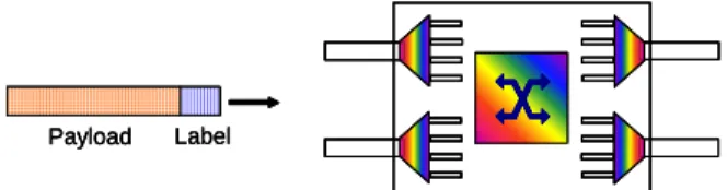
It has been shown that the OT-emulated OBS outperforms the conventional OBS in terms of fairness, scheduling efficiency, QoS provisioning, control and routing operation while conserving main performance characteristics of the conventional one [6-7]. Our labelled OBS has similar characteristics to the OT-emulated OBS but it does not use the BCP. As mentioned previously, we use the Label for carrying routing and burst duration information (Fig.1). A burst is composed of a payload section and a Label. The burst duration ranges from 1 µs to 100 µs. The minimum inter-burst time of 200 ns is defined from the tuning time of the fast tunable laser (FTL) we use. The Label section contains routing (e.g. output port number) and burst duration information. The Label length is 2 bytes in the current version.
Figure 1. Burst composed of a header (Label) and a payload section (Left); Schematic of a 2x2 core node (Right)
Payload Label Payload Label Payload Label
B. Core Switching Node
The switching node is basically a 2x2-node with up to 4 wavelengths per port and is based on a spectral-temporal space switch (Fig.1). It applies a contention resolution strategy resorting to wavelength conversion and temporal delays. The main node functionalities include Label separation and reading, tunable wavelength conversion, tunable optical delays, burst scheduling algorithm and node element control.
III. METRICS TO BE MEASURED
The test bed aims at studying contention resolution mechanisms in a core node. In order to meet this objective, we are planning to measure the following metrics.
• Number of bursts lost, • Throughput,
• Number of bursts dropped due to the lack of FPGA capacity,
• Number of bursts dropped due to the unavailability of optical delay lines,
• Number of bursts dropped due to unsolved contention by the algorithm,
• Number of bursts per second per wavelength, • BER.
IV. TEST BED DESCRIPTION
Fig.2 depicts the test bed we are realising. The test bed is
composed of two parts: OBS node and experimental arrangement. The border materialised by the green dotted dashed line separates these two parts. Outside the line refers to the arrangement for the experiments while inside depicts the structure of a 2x2 switching node with 2 wavelengths per port. IN1,2 refers to input port 1 and 2 respectively. O1,2 refers to
output port 1 and 2 respectively. LExt refers to the label extractor. FDL is fixed fibre delay line that delays incoming bursts the time needed for label processing and TWC configuration (~1.7 µs). TWC refers to the tunable wavelength converter. TDL is tunable delay line. DEMUX is optical demultiplexer. CU is control unit that is based on an FPGA. TXj (λj) is transmitter that generates optical bursts for
experiments.
An incoming optical burst (green-coloured) composed of a 155 Mb/s-label and a 10 Gb/s-payload at wavelength λj arrives
at port IN1. At LExt, the optical label is extracted and
converted to an electronic label (red-coloured). It is sent to CU and its content is read to extract routing and burst duration information. Meanwhile, the incoming burst is optically amplified in LExt and is forwarded to FDL to wait the end of label processing at CU. The processing results in delaying the burst to avoid collision at the output port. According to this decision, CU assigns the burst to output port O1 with λ1 with
the required delay time. Consequently, it sends a control signal to TWCs and a TDL. A TWC (the first one) switches the burst wavelength from λj to λ5 (violet-coloured) and the burst is
forwarded to the λ5 port of DEMUX. The burst at λ5 is again
converted to a burst at λ1 (blue-coloured) by a TWC, and then
is delayed by a TDL before being sent to output port O1.
Frame (burst) loss measurement is done using a burst generator/receiver (Anritsu MT1810A with 2 generators and 4
receivers). It provides TX with electric burst signal and CU with clock signal. All outgoing bursts over the four wavelengths are captured and analysed at the receiver section of MT1810A.
A. Control Unit and Burst Scheduling Algorithm
The control unit is an FPGA from Xilinx (model Vertex-4 LX-60) with 181 I/O ports, clocked at 100 MHz and is capable of handling electronic signals at 155 Mb/s. The FPGA can simultaneously process up to 8 Labels and handle up to 10 wavelengths in approximately 1.7 µs. According to decisions of the scheduling algorithm, the FPGA sends control instructions simultaneously to TWCs and TDLs to configure them. Thus the configuration times are determined by the slowest time that is 200 ns (of fast tunable laser). In addition the FPGA functionality includes event logs that record the number of bursts dropped, the number of TDL unavailability events, and the number of FPGA overload events. Main functions assigned to the FPGA have been tested successfully.
Fig.3 shows the operating principle of our burst scheduling algorithm implemented in the FPGA. The algorithm is LAUC-VF [4-5, 8]. First, the algorithm searches immediately available wavelengths in the wavelength set and if any wavelength is available then checks the availability of tunable delay lines. In case a free delay line is found, the algorithm searches for available wavelengths and selects one that has the least void with the latest forwarded burst.
The request for burst scheduling contains a burst duration value and an output port number. In case of unsuccessful attempt, the request is rejected and the burst is lost while recording the overflow of the tunable delay lines and the request rejection.
Figure 3. Flow Chart of the Scheduling Algorithm
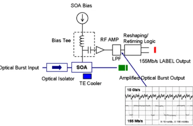
B. Label Extractor
A challenge for implementing Label is its extraction. Label has to be separated from the payload and has to be processed. A straightforward technique would consist in receiving the entire optical burst with an optical burst receiver and then separate electronically the label from the payload. This technique requires a same clock frequency for both Label and
payload sections. When the two sections are clocked at two different frequencies, frequency filtering has to be done before the burst mode electronic CDR (Clock Data Recovery). Having low-frequency-clocked Label might facilitate Label processing. We implement a Label extractor based on a semiconductor optical amplifier (SOA) that can extract a Label clocked at a lower frequency than the payload clock. In addition, SOA can provide additional functions, such as optical amplification and optical input gating when necessary.
It is well known that by observing the terminal voltage of an SOA biased with a constant current source, one can detect an optical intensity variation in the SOA [9]. This phenomenon stems from the fact that incoming photons deplete the conduction band and induce a decrease in quasi-Fermi level separation. This phenomenon is used to extract the label from the burst while amplifying the passing through burst.
In Fig.4, an optical isolator before the SOA prevents from instability due to optical coupling with the network. The SOA is temperature stabilised by a thermo electric element (TE). A constant current is fed to the SOA via a large bandwidth bias tee. Terminal voltage variation from the AC port of the bias tee is amplified by a 40dB-gain RF amplifier and then is low-pass-filtered (≅400 MHz cut-off). A reshaping and retiming logic cleans the 155-Mb/s Label signal. The reshaping and retiming logic delivers LV-PECL signals. The inset figure shows filtered electronic signals at 10 Gb/s and 155 Mb/s. These signals were obtained by feeding PRBS-modulated optical signals to the SOA. The residual amplitude of the 10-Gb/s signal is about the half the 155-Mb/s signal and an additional filtering is still needed.
The SOA is model SOA-S-OEC-1550 from CIP, with an SMA connector. It shows a small signal optical gain of 20 dB at I = 100 mA, λ = 1550 nm, and an electrical bandwidth at the amplified reception of 600 MHz at I = 100 mA, Pi = -10 dBm.
Figure 4. Schematic of the Label Extractor
Fig.5 shows the electrical bandwidth of an SOA biased at 100 mA while feeding different average optical input power at λ = 1530 and 1550 nm. The results are obtained by measuring S21 using a network analyser. It shows the feasibility of label extraction up to 600 MHz bandwidth optical label at -10dBm input power, at 100 mA, at 1550 nm.
REQUEST with burst duration (DB) and output port (PS)
Tunable delay line available? Resources Allocation Request Rejected (Burst Lost) NO NO NO Is λavailable immediately during DB on output port PS? YES
Search for available λ
during DB on output port PS requiring the least optical delay
One or several λ
available? YES
Record an overflow of the tunable delay lines YES
Record rejection of the request Select λshowing the least
void with respect to the latest burst forwarded.
Figure 5. Measured Electrical Bandwidth vs. Average Optical Input Power
C. Tunable WavelengthConverter
The tunable wavelength converter (TWC) being described is of hybrid type in contrast to "all optical" one. In the hybrid TWC, the input optical signal is converted to an electric signal that is used as the modulator driving signal (Fig.6). We use the hybrid TWC due to the following reasons: 1) all optical TWC is expensive, 2) requires high optical signal power, 3) has a narrower tuning range than LiNbO3 modulator, 4) is less stable
than the hybrid TWC unless use of an integrated TWC, 4) a hybrid TWC can regenerate optical signal, and finally 5) the goal of our study is to investigate contention resolution mechanisms in a meshed OBS network and not to develop an all optical TWC.
The input optical burst at λa is converted to an electric burst
by a 10 Gb/s photodiode. The electric signal is amplified and amplitude-limited in a limiter before being sent to a modulator driver. The modulator driver drives a LiNbO3 Mach-Zehnder
(M-Z) modulator of which the operating point is controlled by a modulator bias control circuit. The light from a fast tunable laser (FTL) from INTUNE is modulated by the M-Z modulator. The lasing wavelength of the FTL is assigned by a control signal from the FPGA, for example to λb. Consequently
the TWC converts from λa to λb. 5 wavelength converters were
realised and successfully tested at 10 Gb/s.
The tuning speed of the FTL, which is 200 ns, determines the minimum inter-burst time.
Figure 6. Schematic of the Hybrid Wavelength Converter
D. Tunable Delay Line
Tunable delay line (TDL, actually selectable delay line) allows to adjust the delay of the burst in order to avoid burst collisions in the time domain. Fig.7 shows a TDL with 4 different delays: 0, T, 2T and 3T. The delay is selectable by the SOAG (semiconductor optical amplifier gate) control. SOAGs are driven by the control signals (LV-TTL) from the FPGA and are open or close as a function of the delay value to be selected. The SOAG is composed of a driver and an SOA. The driver is a high speed switching transistor driven by an LV-TTL signal. The driver delivers an ON state current of 90 mA to the SOA. Optical isolators (OI) are inserted to prevent from optical instabilities.
Figure 7. Schematic of the tunable delay line
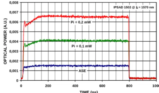
Fig.8 shows gating response of an SOAG driven by a 3-V LV-TTL signal. All of the four SOAG showed 10-11 ns rise times and 2 ns fall times at an average optical input power of -10 dBm. These switching times are short enough for the test bed in which the 200ns tuning time of the fast tunable laser determines the shortest switching time. One important SOAG characteristic is the on-off ratio of optical signal. All the SOAG showed good on-off ratios better than 60 dB at Pi = -10 dBm, λ = 1570 nm.
The SOA is model IPSAD 1502-213 from INPHENIX. It is optimised for switching. The electrical switching time (fall or rise time) is typically 0.5 ns.
Different delay times are obtained by adjusting the length of single mode fibre (SMF). One issue is to prepare fibres with suitable length. The length of fibre has been measured using a delayed sequence identification technique with a precision of ±50 ps. The longest delay is ≤ 100 µs.
Figure 8. Measured gating responses of an SOAG for different powers
0 0,001 0,002 0,003 0,004 0,005 0,006 0,007 0,008 0 200 400 600 800 1000 TIME (ns) O P T IC A L P O W E R ( A .U .) IPSAD 1502 @ λ λ λ λ = 1570 nm ASE Pi = 0,1 mW Pi = 0,2 mW SOAG1 SOAG2 SOAG3 SOAG4 T T 2T
SOAG CONTROL SIGNAL
OI SOAG1 SOAG2 SOAG3 SOAG4 T T 2T
SOAG CONTROL SIGNAL
Figure 9. Picture showing 4-SOAG arrangement
E. Current Test Bed Status
So far main components of the test bed have been realised and tested successfully. Assembling of all components is still in progress. Overall test will be done within a few weeks.
V. SIMULATION TOOL AND ITS PRELIMINARY RESULTS In order to back up the experimental study on the test bed, we have realised a simulation tool. The tool is an event simulator based on OMNET++. It is capable of simulating either labelled or BCP OBS node/networks. It includes the same functionalities as those of the test bed node (in particular the same scheduling algorithm). It can take into account BCP collisions. We actually believe a collision of BCPs results in loss of payload bursts [10]. For traffic generation, it can generate bursts of either uniform or exponential size distribution. The burst arrival is not pre-planned. Instead each port of the node is loaded up to the target value. Main input parameters are:
• Maximum and minimum burst size, • Label (or BCP) length,
• Data and Label line speed, • Number of I/O ports,
• Number of wavelengths per port, • Number of optical delay lines,
• Available delay values (and number) per delay line,
• Label processing times, • FIFO capacity.
Main output metrics/information include: • Input loading indicator (occupied
wavelengths/total wavelengths),
• Number of incoming (and outgoing) bursts per second per wavelength,
• Total number, average size and average offset time of bursts generated,
• Number, average size and average offset time of bursts transmitted,
• Number, average size and average offset time of bursts dropped,
• Number of bursts dropped due to unavailability of delay line,
• Number of bursts dropped due to FIFO overflow, • Number of BCP collisions,
• Number, average size and average offset time of bursts having used delay line,
• Distribution of delay values used.
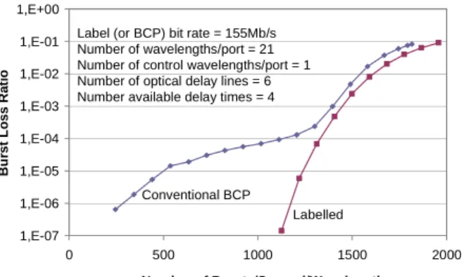
Fig.10 and 11 show examples of simulations made using the tool for a node having 3 input ports and 3 output ports and 21 wavelengths per port. They compare the performance of the Labelled OBS with the conventional BCP OBS when BCP collisions are taken into account. The payload data rate is 10 Gb/s. The scheduling algorithm is the same algorithm as that of the test bed. Other simulation parameters are:
• Payload length and its distribution: 104-107 bits uniformly distributed,
• Label (or BCP) length: 100 bits, • Label (or BCP) speed: 155 Mb/s, • Number of delay lines: 6,
• Selectable delay time values: 1, 10, 100, 1000 µs • BCP carried over one of 21 wavelengths/port. Fig.10 shows the burst loss ratio as a function of number of payload bursts per second per wavelength for the conventional BCP OBS and Labelled OBS schemes. The Labelled OBS outperforms the conventional BCP OBS. High burst loss ratios at low load result from loss of BCP. Detailed explanation on this behaviour is given in [10].
Figure 10. Comparison of Labelled OBS with conventional BCP OBS: payload burst loss ratio vs. number of bursts/second/wavelength Fig.11 shows the burst loss ratio as a function of occupation ratio (occupied λ/total λ). For the conventional BCP OBS scheme, 20 wavelengths are used for payload transfer.
1,E-07 1,E-06 1,E-05 1,E-04 1,E-03 1,E-02 1,E-01 1,E+00 0 500 1000 1500 2000 Nomber of Bursts/Second/Wavelength B u rs t L o s s R a ti o
Label (or BCP) bit rate = 155Mb/s Number of wavelengths/port = 21 Number of control wavelengths/port = 1 Number of optical delay lines = 6 Number available delay times = 4
Labelled Conventional BCP
Therefore the total number of wavelengths is 20 for the conventional BCP scheme. For the Labelled OBS scheme, this value is 21. Again, BCP loss increases the burst loss ratio at low occupation in the conventional BCP OBS scheme.
Figure 11. Comparison of Labelled OBS with conventional BCP OBS: payload burst loss ratio vs. wavelength occupancy
VI. CONCLUSIONS AND PROSPECTS
We have described our test bed for studying contention resolution mechanisms. The test bed is composed of an OBS core node and apparatus for measurements. The 2x2 OBS core node with 2λ/port is capable of switching 1-100 µs duration asynchronous bursts using a spectral-temporal space switch. The burst is composed of a header (called Label) and a payload section. The Label carries information on output port and burst duration and allows routing of the burst. Main components of the test bed have been realised and tested successfully. A burst scheduling algorithm, which is implemented in an FPGA and passed preliminary test, will decrease burst contention thanks to TWCs and TDLs. Assembling of all components is still in progress.
A simulation tool aiming at backing up the experimental study was described together with a preliminary study that compared the Labelled OBS scheme with the conventional
BCP OBS scheme. The results showed that the Labelled OBS scheme outperformed the conventional BCP OBS scheme.
The foreseeing work consists in achieving the test bed and in evaluating experimentally the efficiency of the burst scheduling algorithm implemented in the FPGA. Experimental results will be compared with simulation predictions.
ACKNOWLEDGMENT
This work was in part supported by the European Commission through the IST IP NOBEL 2 project (FP6-027305). The authors thank Thierry Guillossou for his valuable contributions to the test bed realization and Paul Ghobril for his efficient technical assistance in the simulation tool realization.
REFERENCES
[1] C. Qiao, M. Yoo, "Optical burst switching (OBS) – a new paradigm for an optical Internet", J. High Speed Networks, vol.8, no.1, pp.69-84, Mar. 1999.
[2] Y. Chen, C. Qiao, X. Yu, "Optical burst switching: a new area in optical networking research", IEEE Network, pp.16-23, May/June 2004. [3] C. Qiao, "Labeled optical burst switching for IP-over-WDM
integration", IEEE Commun. Mag., vol.38, no.9, pp.104-114, Sept. 2000.
[4] S. J. B. Yoo, "Optical packet and burst switching technologies for the future photonic Internet", J. Lightwave Technol. Vol.24, no.12, pp.4468-4492, Dec. 2006.
[5] T. Legrand, "Réalisation de banc d'essai pour l'étude des contentions de bursts de données", JNOG 2007, Grenoble, France, 2007.
[6] M. Klinkoski, D. Careglio, J. Solé-Pareta, "Offset-time emulated OBS control architecture", paper Tu3.6.1, ECOC 2006, 2006.
[7] M. Klinkoski, D. Careglio, J. Solé-Pareta, "Comparison of conventional and offset time-emulated optical burst switching architectures", paper Mo.C3.6, ICTON 2006, 2006.
[8] J. Xu et al., "Efficient channel scheduling algorithm in optical burst switching networks", IEEE INFOCOM 2003, 2003.
[9] M. Gustavsson, A. Karlsson, L. Thylen, "Travelling wave semiconductor laser amplifier detectors", IEEE J. Lightwave Technolo. Vol.8, no.4, pp.610-617, April 1990.
[10] T. Legrand, H. Nakajima, P. Gavignet, B. Cousin, "Comparaison de l'OBS conventionnel et de l'OBS à Label", submitted to JNOG 2008, 2008. 1,E-07 1,E-06 1,E-05 1,E-04 1,E-03 1,E-02 1,E-01 1,E+00 0 0,2 0,4 0,6 0,8 1
Occupied Wavelengths/Total Number of Wavelengths
B u rs t L o s s R a ti o
Label (or BCP) bit rate = 155Mb/s Number of wavelengths/port = 21 Number of control wavelengths/port = 1 Number of optical delay lines = 6 Number available delay times = 4
Conventional BCP